
G.983.1 Option2 FSAN OLT Transceiver
OAT1521S-OLT2-V2-B
Oki Electric Industry Co., Ltd.
1/
December/2001
Document NO: QPS-0201-056
Rev. DRAFT 0.1
G.983.1 Option2 FSAN OLT
Transceiver Specifications
Part Number : OAT1521S-OLT2-V2-B
ITU-T G.983.1 Option2 Class B acceptable
Modification History
Rev.
Date
Originator
Comment
DRAFT0.1
Dec. 19 , 2001
H. OKADA
1. Specifications
Table 1.1 Specifications
Parameter
Unit
Specifications
Bit rate
Mbit/s
Tx:622.08 , Rx:155.52
Transmission mode
-
Tx: continuous, Rx: burst
Transfer code
-
NRZ
Bi-directional transmission
-
1-fibre WDM
Transmission distance
km
20
Laser diode
-
1.55um DFB-LD
photo detector
-
PIN-PD
Operating temperature range
∞
C
0 ~ 70
Operating humidity
%
5 ~ 90
Fiber/Connector type
-
Single mode fiber (10/125nm) / PC polished SC connector
Power supply voltage
V
+3.3 +/-5%
Power consumption
W
1.2 (typ.) , 1.4(max.)
Dimension
mm
40
◊
60
◊
8.5
Document Number QPS-0201-056
Revision DRAFT 0.1
DATE: December. 19, 2001
Author H. OKADA
Project Manager K. YUSA

G.983.1 Option2 FSAN OLT Transceiver
OAT1521S-OLT2-V2-B
Oki Electric Industry Co., Ltd.
2/
December/2001
Document NO: QPS-0201-056
Rev. DRAFT 0.1
Table 1.2 Optical Characteristics (over operating temperature and lifetime)
Parameter
Unit
Specifications
Operating wavelength
nm
Tx:1480 - 1580 / Rx:1260 - 1360
Mask of the transmitter eye diagram
ITU-T G.983 Downstream
Maximum reflectance of equipment, measured at
transmitter wavelength
dB
-
Mean launched power range
dBm
SOL -1.5 ~ +4.0
EOL -2.0 ~ +4.0
Minimum extinction ratio
dB
10
Tolerance to the transmitter incident light
power
dB
more than -15
Launched optical power
w/o input to the transmitter
dBm
-
Maximum spectral width
nm
1 (@-20dB)
Side mode suppression ratio
dB
more than 30
Jitter transfer
-
Jitter generation in 1.3kHz bandwidth
UIpp
-
Maximum reflectance of equipment,
measured at receiver wavelength
dB
less than -20
Bit error ratio
-
less than 10
-10
Minimum sensitivity
dBm
SOL -30.5
EOL -30.0
Minimum overload
dBm
SOL -7.5
EOL -8.0
Consecutive identical digit immunity
-
more than 72
Jitter tolerance
-
-
Tolerance to the reflected optical power
dB
less than 10
Table 1.3 Absolute maximum ratings
Parameter
Symbol
Conditions
Ratings
Unit
Power supply voltage
Vcc
0 to +4.6
V
Input voltage
Vi
0 to Vcc
V
Maximum output current
Io
Ta = 25
∞
C
30
mA
Storage temperature
Tstg
-40 to +85
∞
C
Soldering temperature/time
Ta = 25
∞
C
250/10
∞
C/sec
Maximum tension of fiber
500
g
Minimum bending radius
30
mm

G.983.1 Option2 FSAN OLT Transceiver
OAT1521S-OLT2-V2-B
Oki Electric Industry Co., Ltd.
3/
December/2001
Document NO: QPS-0201-056
Rev. DRAFT 0.1
2. Block diagram
Fig. 2.1 Block diagram
PD
LD
PD
LD Driver
APC
D-FF
TF
1310nm
OPT I/O
1310nm/1550nm
WDM
CLK IN
DATA IN
SHUT IN
CDR
ATC
Pre-amp
1550nm
DATA OUT
CLK OUT
SYNC. LOSS
TD
CD
CDR RESET IN
ATC RESET IN
POC IN
Clk Detection
G.983.1 Option2 FSAN OLT Transceiver
OAT1521S-OLT2-V2-B
Oki Electric Industry Co., Ltd.
4/
December/2001
Document NO: QPS-0201-056
Rev. DRAFT 0.1
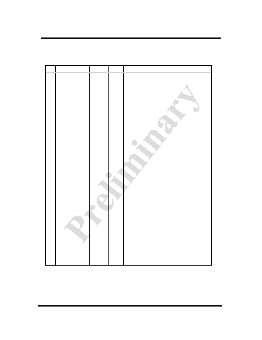
3. Pin description
Table 3.1 Pin descriptions
No. I/O Symbol
Level Logic Functionality
01
SVCC
Transmitter power supply (+3.3V)
02
GND
Ground
03
I SDATAP
LVPECL
Data input (pos) :622.08Mbps
04
I SDATAN
LVPECL
P
Data input (neg) :622.08Mbps
05
I BCLKP
LVPECL
CDR Clock input (pos) :155.52Mbps
06
I BCLKN
LVPECL
P
CDR Clock input (neg) :155.52Mbps
07
GND
Ground
08
I SHUT
LVTTL
P
Optical output shut down
09 O CD
LVTTL
P
Clock down alarm (All'L')
10 O TD
LVTTL
P
Transmitter Degraded alarm
11 O TF
LVTTL
P
Transmitter Failure alarm
12
GND
Ground
13
GND
Ground
14 O ALM
LVTTL
P
Sync. out alarm
15
GND
Ground
16
I POC
LVTTL
N Power on clear
17
I BRSP
LVPECL
CDR reset (pos)
18
I BRSN
LVPECL
N
CDR reset (neg)
19
GND
Ground
20 O RCLKP
LVPECL
Clock output (pos)
21 O RCLKN
LVPECL
P
Clock output (neg)
22
GND
Ground
23 O RDATAP
LVPECL
Data output (pos)
24 O RDATAN
LVPECL
P
Data output (neg)
25
GND
Ground
26
BVCC
Power supply for CDR (+3.3V)
27
GND
Ground
28
GND
Ground
29
I RSN
LVPECL
ATC reset (neg)
30
I RSP
LVPECL
N
ATC reset (pos)
31
GND
Ground
32
RVCC
Power supply for ATC (+3.3V)

G.983.1 Option2 FSAN OLT Transceiver
OAT1521S-OLT2-V2-B
Oki Electric Industry Co., Ltd.
5/
December/2001
Document NO: QPS-0201-056
Rev. DRAFT 0.1
4. Outline
(1)
(12)
(32)
(13)
30.32±0.3
12 -
0
.45
19x1.27
=24.13±0.3
7.775
8.5MAX
(3.39)
13x2.54 = 33.02±0.3
(3.39)
(7.8)
20 -
0
.45
40±1
60±1
(TOP View)
0.8
1.27
(3.1)
(4.9)
(6.6)
(0.4)
(3.29)
3.29
(3.6)
33.0 ± 0.3
39.6 ± 0.3
(38)
L
(10)
27.9
(4.125)
12.1
Fig 4.1 Package Outline