FSAN ONU/ONT Transceiver ≠G983.1/3 and Option1(OC3) ClassB
Document NO: QPS-0202-026
Rev.1
Oki Electric Industry Co., Ltd.
1/12
FSAN ONU/ONT Optical Transceiver
-G983.1/3 Option.1 (OC3) ClassB-
OAT1521S-ONU-V4-B-10
Data Sheet
Modification History
Rev.
Date
Author / Project Manager
Comment
Rev.1
Jun.5, 2002
H. Okada / K. Yusa
FSAN ONU/ONT Transceiver ≠G983.1/3 and Option1(OC3) ClassB
Document NO: QPS-0202-026
Rev.1
Oki Electric Industry Co., Ltd.
2/12
1. General Description
The OAT1521S-ONU-V4-B-10 optical transceiver is compliant with recommendation of ITU-T G.983.1
/ 983.3 option1 class B for use in ATM-PON application. It is applicable for the optical interface of the ONU
/ONT which is located on the subscriber side. These modules have the following functions.
-1-fiber bi-directional transmission by incorporated wavelength division multiplexer (WDM).
-Conversion of 156Mbit/s electric signal to 1.3um optical signal by laser diode (E/O conversion).
-Stabilization of optical output power and waveform with laser diode driving current temperature
compensation circuit.
-Transmit failure (TF) detection.
-Optical signal output shut down (LS).
-Conversion of 156Mbit/s 1.55um optical signal to electric signal by PIN-photo diode (O/E conversion).
- w/ CDR function
-Incoming signal lost detection (LOS).
The specifications are shown on the table 1.1
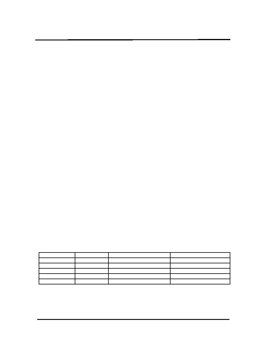
Table1.1 Specifications
Parameter
Unit
OAT1521S-ONU-V4-B-10
Bit rate
Mbps
Up-stream:155.52
Down-stream:155.52
Transmission mode
-
Tx: burst
Rx: continuous
Transfer code
-
NRZ
Bi-directional transmission
-
1-fibre WDM
Transmission distance
km
20
Laser diode
-
1.31nm FP-LD
photo detector
-
PIN-PD
Operating temperature range
∞C
-40 to 85
Operating humidity
%
5 to 90
Fiber/Connector type
-
Single mode fiber (10/125um) /
PC polished SC connector
Power supply voltage
V
+3.3 +/- 5%
Power consumption
W
1.1 (typ.) ,1.5(max)
Dimension
mm
40 x 60 x 9.5

FSAN ONU/ONT Transceiver ≠G983.1/3 and Option1(OC3) ClassB
Document NO: QPS-0202-026
Rev.1
Oki Electric Industry Co., Ltd.
3/12
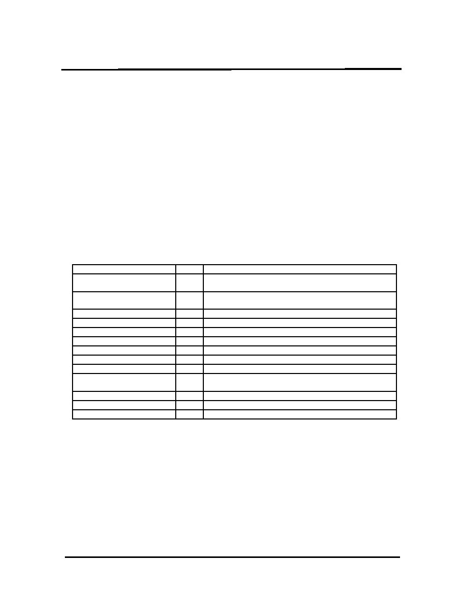
2. Absolute Maximum Ratings
Stress in excess of the maximum absolute ratings can cause permanent damage to the module.
Table2.1 Absolute maximum ratings
Parameter
Symbol Conditions
Ratings
Unit
Power supply voltage
Vcc
0 to +4.6
V
Input voltage
Vi
0 to Vcc
V
Maximum output current
Io
Ta = 25∞C
30
mA
Operating temperature
Top
ONU:-40 to +85
∞C
Storage temperature
Tstg
-40 to +85
∞C
Soldering temperature/time
250/10
∞C/sec
Maximum tension of fiber
500
g
Minimum bending radius
30
mm
Maximum optical input power
Ta = 25∞C
0
dBm
3.Block diagram
Figuer3.1 Block diagram (OAT1521S-ONU-V4-B-10)
PD
LD
PD
LD Driver
Temp.
Compensation
D-FF
TF
Alarm
1310nm
OPT I/O
1550nm/1310nm
WDM
CLK IN
DATA IN
PRE-BIAS IN
SHUT IN
Retiming
Regenerating
Reshaping
Pre-amp
1550nm
DATA OUT
CLK OUT
LOS
FSAN ONU/ONT Transceiver ≠G983.1/3 and Option1(OC3) ClassB
Document NO: QPS-0202-026
Rev.1
Oki Electric Industry Co., Ltd.
4/12
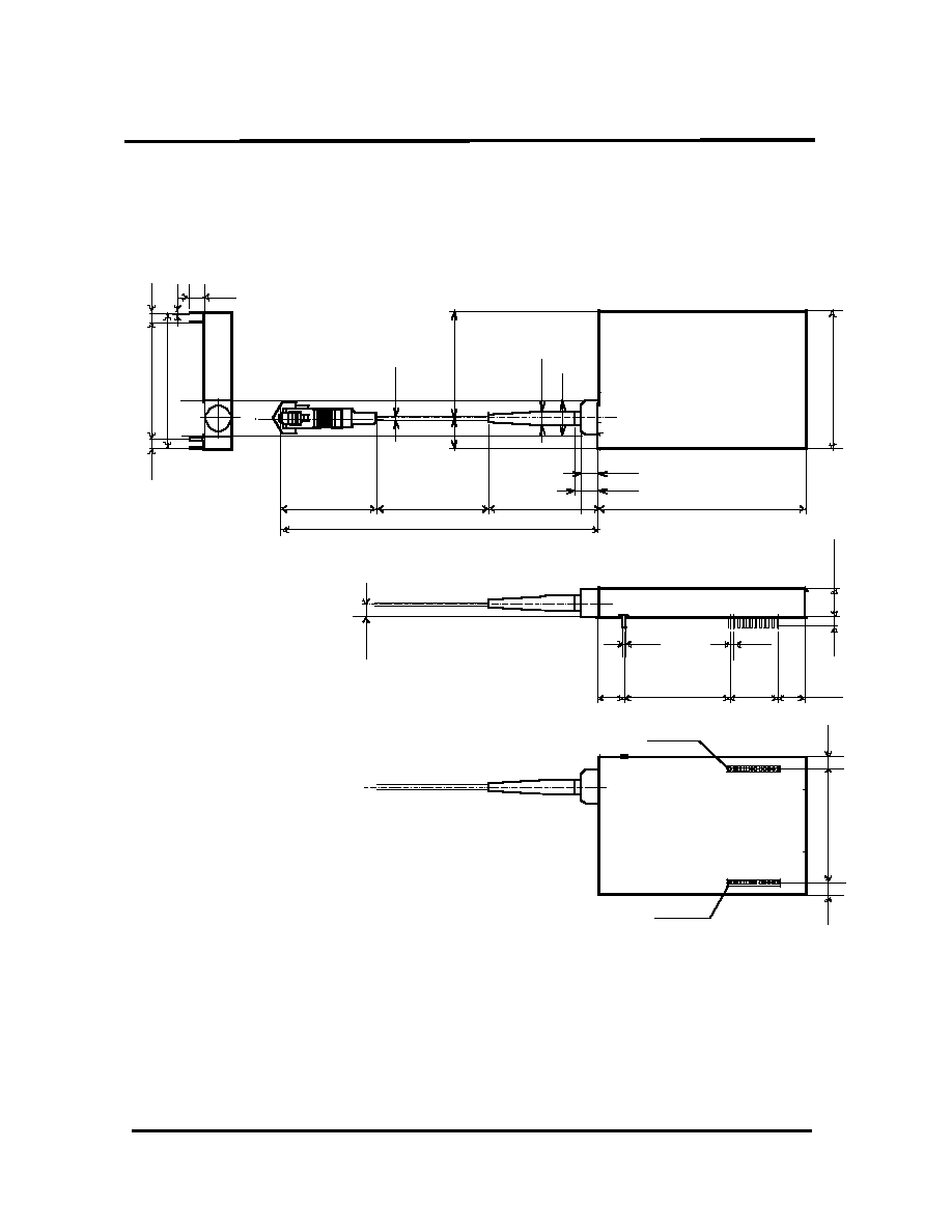
4.Package outline
30.455±0.3
12-0.45
11x1.27
=13.97±0.3
7.775
9.5MAX
(1)
(12)
(3.39)
13x2.54=33.02±0.3
(24)
(13)
(3.39)
(7.8)
( Bottom View)
12-0.45
(0.4)
(3.29)
3.29
(3.6)
33.02±0.3
39.6±0.3
40±1
60±1
(TOP View)
0.8
1.27
(3.1)
(38)
(928
+200
-200
)
998
+200
-200
(32)
(4.9)
(6.6)
0.9
(31)
9
(4.125)
(
4.2)
(10)
Figure4.2 (OA1521S-ONU-V4-B-10)

FSAN ONU/ONT Transceiver ≠G983.1/3 and Option1(OC3) ClassB
Document NO: QPS-0202-026
Rev.1
Oki Electric Industry Co., Ltd.
5/12
5. Pin description
Table 5.1 Pin descriptions (OAT1521S-ONU-V4-B-10)
No. I/O Symbol
Level
Logic Functionality
01
SVCC
Transmitter power supply (+3.3V)
02
GND
Ground
03
I SHUT
LVTTL
P
Optical output shut down
04
O TF
LVTTL
P
Transmitter Failure alarm
05
GND
Ground
06
I BIASP
LVPECL
Pre-bias input(pos)
07
I BIASN
LVPECL
P
Pre-bias input(neg)
08
GND
Ground
09
I SDATAP LVPECL
Data input(pos)
10
I SDATAN LVPECL
P
Data input(neg)
11
I SCLKP
LVPECL
Clock input(pos)
12
I SCLKN
LVPECL
P
Clock input(neg)
13
GND
Ground
14
O LOS
LVTTL
P
Loss of incoming signal alarm
15
GND
Ground
16
O RDATAN LVPECL
Data output (neg)
17
O RDATAP LVPECL
P
Data output (pos)
18
GND
Ground
19
O RCLKN
LVPECL
Clock output (neg)
20
O RCLKP
LVPECL
P
Clock output (pos)
21
GND
Ground
22
GND
Ground
23
RVCC1
Receiver power supply (+3.3V)
24
RVCC2
Receiver power supply (+3.3V)