
FSAN ONU/ONT Transceiver ≠G983.1/3 and Option1(OC3) ClassC
Document NO: QPS-0202-056
Rev.1
Oki Electric Industry Co., Ltd.
1/12
FSAN ONU/ONT Optical Transceiver
-G983.1/3 Option.1(OC3) ClassC-
OAT1521S-ONU-V3-C-06
Data Sheets
Modification History
Rev.
Date
Author / Project Manager
Comment
Rev.1
Sep.9, 2002
H. Okada / K. Yusa

FSAN ONU/ONT Transceiver ≠G983.1/3 and Option1(OC3) ClassC
Document NO: QPS-0202-056
Rev.1
Oki Electric Industry Co., Ltd.
2/12
1. General Description
The OAT1521S-ONU-V3-C-06 optical transceiver is compliant with recommendation of ITU-T G.983.1
/ 983.3 option1 class B for use in ATM-PON application. It is applicable for the optical interface of the ONU
/ONT which is located on the subscriber side. These modules have the following functions.
-1-fiber bi-directional transmission by incorporated wavelength division multiplexer (WDM).
-Conversion of 156Mbit/s electric signal to 1.3um optical signal by laser diode (E/O conversion).
-Stabilization of optical output power and waveform with laser diode driving current temperature
compensation circuit.
-Transmit failure (TF) detection.
-Optical signal output shut down (LS).
-Conversion of 156Mbit/s 1.55um optical signal to electric signal by PIN-photo diode (O/E conversion).
- w/ CDR function
-Incoming signal lost detection (LOS).
The specifications are shown on the table 1.1
Table1.1 Specifications
Parameter
Unit
OAT1521S-ONU-V3-C-06
Bit rate
Mbps
Up-stream:155.52
Down-stream:155.52
Transmission mode
-
Tx: burst
Rx: continuous
Transfer code
-
NRZ
Bi-directional transmission
-
1-fibre WDM
Transmission distance
km
20
Laser diode
-
1.31nm FP-LD
photo detector
-
PIN-PD
Operating temperature range
∞C
-40 to 85
Operating humidity
%
5 to 90
Fiber/Connector type
-
Single mode fiber (10/125um) /
PC polished SC connector
Power supply voltage
V
+3.3 +/- 5%
Power consumption
W
1.1 (typ.) ,1.5(max)
Dimension
mm
40 x 60 x 9.5

FSAN ONU/ONT Transceiver ≠G983.1/3 and Option1(OC3) ClassC
Document NO: QPS-0202-056
Rev.1
Oki Electric Industry Co., Ltd.
3/12
2. Absolute Maximum Ratings
Stress in excess of the maximum absolute ratings can cause permanent damage to the module.
Table2.1 Absolute maximum ratings
Parameter
Symbol Conditions
Ratings
Unit
Power supply voltage
Vcc
0 to +4.6
V
Input voltage
Vi
0 to Vcc
V
Maximum output current
Io
Ta = 25∞C
30
mA
Operating temperature
Top
ONU:-40 to +85
∞C
Storage temperature
Tstg
-40 to +85
∞C
Soldering temperature/time
250/10
∞C/sec
Maximum tension of fiber
500
g
Minimum bending radius
30
mm
Maximum optical input power
Ta = 25∞C
0
dBm
3.Block diagram
Figuer3.1 Block diagram (OAT1521S-ONU-V3-C-06)
PD
LD
PD
LD Driver
Temp.
Compensation
D-FF
TF
Alarm
1310nm
OPT I/O
1490or1550nm
/1310nm
WDM
CLK IN
DATA IN
PRE-BIAS IN
SHUT IN
Retiming
Regenerating
Reshaping
Pre-amp
1490/
1550nm
DATA OUT
CLK OUT
LOS

FSAN ONU/ONT Transceiver ≠G983.1/3 and Option1(OC3) ClassC
Document NO: QPS-0202-056
Rev.1
Oki Electric Industry Co., Ltd.
4/12
4.Package outline
30.455±0.3
12-
0.45
11x1.27
=13.97±0.3
7.775
8.5MAX
(1)
(12)
(3.39)
13x2.54=33.02±0.3
(24)
(13)
(3.39)
(7.8)
( Bottom View)
12-
0.45
40±1
60±1
(TOP View)
0.8
1.27
(3.1)
(0.4)
(3.39)
3.39
(3.1)
33.02±0.3
39.8±0.3
(38.5)
618 ± 15
27.9
(5.74)
12.1
0.9
(0.85)
Figure4.2 (OAT1521S-ONU-V3-C-06)

FSAN ONU/ONT Transceiver ≠G983.1/3 and Option1(OC3) ClassC
Document NO: QPS-0202-056
Rev.1
Oki Electric Industry Co., Ltd.
5/12
5. Pin description
Table 5.1 Pin descriptions (OAT1521S-ONU-V3-C-06)
No. I/O Symbol
Level
Logic Functionality
01
SVCC
Transmitter power supply (+3.3V)
02
GND
Ground
03
I SHUT
LVTTL
P Optical output shut down
04 O TF
LVTTL
P Transmitter Failure alarm
05
GND
Ground
06
I BIASP
LVPECL
Pre-bias input(pos)
07
I BIASN
LVPECL
P
Pre-bias input(neg)
08
GND
Ground
09
I SDATAP LVPECL
Data input(pos)
10
I SDATAN LVPECL
P
Data input(neg)
11
I SCLKP
LVPECL
Clock input(pos)
12
I SCLKN LVPECL
P
Clock input(neg)
13
GND
Ground
14 O LOS
LVTTL
P Loss of incoming signal alarm
15
GND
Ground
16 O RDATAN LVPECL
Data output (neg)
17 O RDATAP LVPECL
P
Data output (pos)
18
GND
Ground
19 O RCLKN LVPECL
Clock output (neg)
20 O RCLKP LVPECL
P
Clock output (pos)
21
GND
Ground
22
GND
Ground
23
RVCC1
Receiver power supply (+3.3V)
24
RVCC2
Receiver power supply (+3.3V)

FSAN ONU/ONT Transceiver ≠G983.1/3 and Option1(OC3) ClassC
Document NO: QPS-0202-056
Rev.1
Oki Electric Industry Co., Ltd.
6/12
6.Optical and electrical characteristics
Table6.1 Optical characteristics
Parameter
Unit
OAT1521S-ONU-V3-C-06
Operating wavelength
nm
Tx: 1260 ~ 1360
Rx: 1480 ~ 1580
Mask of the transmitter eye
diagram
Figure6.1
Maximum reflectance of equipment,
measured at transmitter wavelength
dB
less than -6
Mean launched power range
dBm
SOL: -1.5 to +4.0/EOL: -2.0 to +4.0
Minimum extinction ratio
dB
10
Tolerance to the transmitter
incident light power
dB
more than -15
Launched optical power
w/o input to the transmitter
dBm
less than ≠43
Maximum spectral width
nm
5.8 (@rms)
Side mode suppression ratio
dB
-
Jitter transfer
0.1 (fc=130kHz)
Figure6.2
Jitter generation in 1.3kHz
bandwidth
UIpp
0.2
Maximum reflectance of
equipment, measured at
receiver wavelength
dB
less than -20
Bit error ratio
-
less than 10
-10
Minimum sensitivity
dBm
SOL: -33.5 /EOL: -33.0
Minimum overload
dBm
SOL: -7.5/EOL: -8.0
Consecutive identical digit
immunity
-
more than 72
Jitter tolerance
-
Figure6.3
Tolerance to the reflected
optical power
dB
More than -10

FSAN ONU/ONT Transceiver ≠G983.1/3 and Option1(OC3) ClassC
Document NO: QPS-0202-056
Rev.1
Oki Electric Industry Co., Ltd.
7/12
Table6.2 Electrical characteristics
Parameter
Unit
OAT1521S-ONU-V3-C-06
MIN
TYP
MAX
PECL input high voltage
VCC-1.17
VCC-0.88
PECL input low voltage
VCC-1.81
VCC-1.47
PECL output high voltage
VCC-1.02
VCC-0.88
PECL output low voltage
VCC-1.81
VCC-1.62
LVTTL input high voltage
2.0
Vcc+0.3
LVTTL input low voltage
-0.3
0.8
LVTTL output high voltage
2.4
Vcc
LVTTL output low voltage
V
0
0.4
Clock input duty
%
40
50
60
Data output rise/fall time
( 20 - 80 % )
ns
1.2
Clock/Data input setup &
hold time
Figure6.4
Clock/Data output timing
Figure6.5
Data/Prebias Input Timing
Figure6.6
Figure6.1 Eye pattern mask
(0.35,0.2)
(0.5,0.13)
(0.65,0.2)
(0.5,0.87)
Mean level of
logical "0"
Mean level of
logical "1"
Amplitude
UI
(0,0)
(1.0,0)
(0.1,0.5)
(0.65,0.8)
(0.5,1.0)
(0.5,0)
(0.5,1.13)
(0.5,-0.13)
(0.9,0.5)
(1.0,1.0)
(0.35,0.8)
(0,1.0)
(0.35,0.2)
(0.5,0.13)
(0.65,0.2)
(0.5,0.87)
Mean level of
logical "0"
Mean level of
logical "1"
Amplitude
UI
(0,0)
(1.0,0)
(0.1,0.5)
(0.65,0.8)
(0.5,1.0)
(0.5,0)
(0.5,1.13)
(0.5,-0.13)
(0.9,0.5)
(1.0,1.0)
(0.35,0.8)
(0,1.0)

FSAN ONU/ONT Transceiver ≠G983.1/3 and Option1(OC3) ClassC
Document NO: QPS-0202-056
Rev.1
Oki Electric Industry Co., Ltd.
8/12
Figure6.2 Jitter transfer
Figure6.3 Jitter tolerance
Slope = 20dB/dec
Frequency
130kHz
Jitter gain [dB]
0.1
6.5kHz
65kHz
Slope = 20dB/dec
Frequency
Input jitter amplitude [UIp-p]
0.075
0.75

FSAN ONU/ONT Transceiver ≠G983.1/3 and Option1(OC3) ClassC
Document NO: QPS-0202-056
Rev.1
Oki Electric Industry Co., Ltd.
9/12
This timing is based on the data cross point
Figure6.4 Clock/Data, Bias input setup & hold time
This timing is based on the data cross point.
Figure6.5 Clock/Data output timing
t
stup
t
hld
Data,Bias
Input
Clock Input
t
stup
1.2 ns
t
hld
1.2 ns
Clock output
Data output
t
OAT1521S-ONU-V3-C-06 : 0.8ns
t
1.8ns

FSAN ONU/ONT Transceiver ≠G983.1/3 and Option1(OC3) ClassC
Document NO: QPS-0202-056
Rev.1
Oki Electric Industry Co., Ltd.
10/12
Figure6.6 Up-stream Data/Bias signal input timing
t
T1
T2
Up-Stream DATA Input
Bias(P) Input
T1 > 2bits
T2 = 0bit
t
T1
T2
Up-Stream DATA Input
Bias(P) Input
T1 > 2bits
T2 = 0bit
FSAN ONU/ONT Transceiver ≠G983.1/3 and Option1(OC3) ClassC
Document NO: QPS-0202-056
Rev.1
Oki Electric Industry Co., Ltd.
11/12
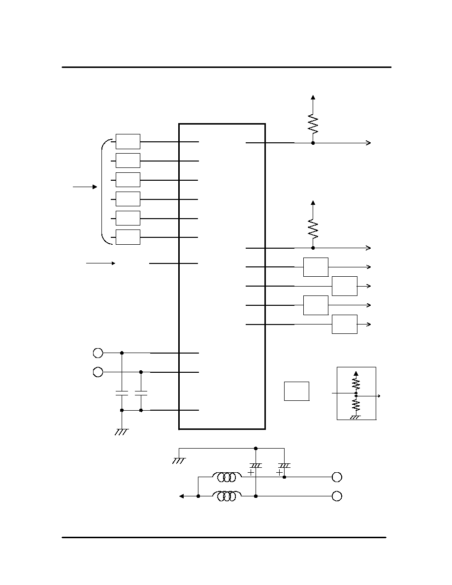
7. Recommended interface circuit
Figure7.1 Recommended interface circuit
03
SDATAP
12
11
10
09
SDATAN
SCLKP
SCLKN
SHUT
02,05,08,13,
15,18,21,22
23,24
01
20
SVCC
RVCC
OAT1521S-ONU-V3-C-06
LV-PECL
INPUT
TF
LOS
RDATAP
RDATAN
RCLKP
RCLKN
14
17
19
16
04
+3.3V
GND
1.6k
1.6k
0.1µF
0.1µF
RVCC
SVCC
22µF
22µF
22µH
22µH
SVCC
RVCC
+3.3V
+3.3V
Ztrm
Ztrm
Ztrm
Ztrm
Ztrm
=
LVTTL INPUT
BIASP
BIASP 07
06
+3.3V
130
82
Ztrm
Ztrm
Ztrm
Ztrm
Ztrm
Ztrm

FSAN ONU/ONT Transceiver ≠G983.1/3 and Option1(OC3) ClassC
Document NO: QPS-0202-056
Rev.1
Oki Electric Industry Co., Ltd.
12/12
8. Precautions for handling
The circuits of these modules operate at very small signal. In order to avoid the degradation of the
optical sensitivity due to external noise, the bottom pattern of these modules on the PCB should be ground
pattern with low impedance.
Do not mount/pattern device/circuits which generate high frequency noise close to the module.
In order to operate the module stable against the power noise, install the power supply noise reduction
circuits.
The impedance between the power and ground pattern of the power circuit should be as low as possible. The
elements around the module should be mounted close to the pins of the module.
If an optical power exceeding the absolute maximum ratings is fed to the module, the optical receiver may be
damaged. Set the optical input power appropriately when in use of these modules.
9. Qualification and Reliability
To help ensure high product reliability and customer satisfaction, OKI is committed to an intensive quality
program that starts in the design phase and proceeds through the manufacturing process.
Optical transceiver modules are qualified to OKI internal standards using MIL-STD-883 test methods and
procedures and using sample techniques consistent with Telcordia requirements.
This qualification program fully meets the intent of Telcordia reliability practices GR-468-CORE.
10. Laser Safety
All version of transceiver are Class 1 Laser products FDA complies with 21 CFR 1040.10 and 1040.11
requirements.
Also, all versions are Class 1 Laser products pre IEC 825-1.