Ether-PON OLT Transceiver Preliminary
Specifications
Document NO: QPS-0202-068
Rev. DRAFT0.1
Oki Electric Industry Co., Ltd.
1/8
Preliminary
Ether-PON w/o OLT Transceiver
Specifications
Part Number : OAT6222S-OLT-V4-B
Modification History
Rev.
Date
Originator
Comment
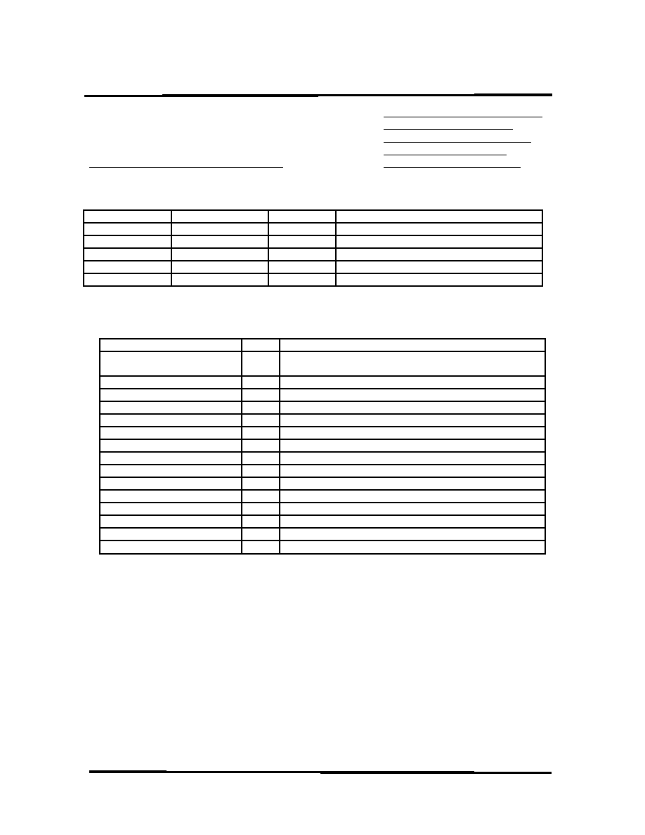
1.Specifications
Table 1.1 Specifications
Parameter
Unit
Specifications
Bit rate
Mbit/
s
622.08
Transmission mode
-
Tx: continuous, Rx: burst
Transfer code
-
NRZ
Bi-directional transmission
-
1-fibre WDM
Transmission distance
km
20 (Max.)
Laser diode
-
1.55um DFB-LD
Photo detector
-
APD
Attenuation range
dB
10 � 25
Path penalty
dB
1
Operating temperature range
�C
0 ~ 70
Operating humidity
%
5 ~ 95
Fiber/Connector type
-
Single mode fiber (10/125nm) / PC polished SC connector
Power supply voltage
V
+3.3V � 5%
Power consumption
W
2.0W (Typ.) , 2.5W (Max)
Dimension
mm
70�~
50�~
9.5
Document Number QPS-0202-068
Revision Draft0.1
DATE: October. 22, 2002
Author H. Okada
Project Manager K. YUSA

Ether-PON OLT Transceiver Preliminary
Specifications
Document NO: QPS-0202-068
Rev. DRAFT0.1
Oki Electric Industry Co., Ltd.
2/8
Preliminary
Table 1.2 Optical Characteristics (over operating temperature and lifetime)
Parameter
Unit
Specifications
Part number
OAT6222S-OLT-V4-B
Operating wavelength
nm
Tx:1480 - 1580/Rx:1260 -1360
Mask of the transmitter eye diagram
Figure1.1
Maximum reflectance of equipment, measured at
transmitter wavelength
dB
-
Mean launched power range
dBm
-2.0 ~ +4.0
Minimum extinction ratio
dB
10
Tolerance to the transmitter incident light
power
dB
more than -15
Launched optical power
w/o input to the transmitter
dBm
-
Maximum spectral width
nm
1.0 (@-20dB)
Side mode suppression ratio (@DFB-LD)
dB
More than 30
Jitter transfer
dB
-
Jitter generation in 1.3kHz bandwidth
UIpp
-
Maximum reflectance of equipment,
measured at receiver wavelength
dB
less than -20
Bit error ratio
-
less than 10
-12
Minimum sensitivity
dBm
-27.0
Minimum overload
dBm
-6.0
Consecutive identical digit immunity
bit
more than 72
Jitter tolerance
-
-
Tolerance to the reflected optical power
dB
less than 10
Note
:
A noise possibility appears at the back of each packets.
Table 1.3 Absolute maximum ratings
Parameter
Symbol
Conditions
Ratings
Unit
Power supply voltage
Vcc
0 to +7.0
V
Input voltage
Vi
0 to Vcc
V
Maximum output current
Io
Ta = 25�C
30
mA
Storage temperature
Tstg
-40 to +85
�C
Soldering temperature/time
Ta = 25�C
250/10
�C/sec
Maximum tension of fiber
500
g
Minimum bending radius
30
mm

Ether-PON OLT Transceiver Preliminary
Specifications
Document NO: QPS-0202-068
Rev. DRAFT0.1
Oki Electric Industry Co., Ltd.
3/8
Preliminary
Figure1.1 Eye mask pattern for OAT6222S-OLT
Table1.4 DC characteristic
Parameter
Unit
OAT6222S-OLT-V4-B
MIN
TYP
MAX
PECL input high voltage
VCC-1.17
-
VCC-0.88
PECL input low voltage
VCC-1.81
-
VCC-1.47
PECL output high voltage
VCC-1.02
-
VCC-0.88
PECL output low voltage
VCC-1.81
-
VCC-1.62
LVTTL input high voltage
2.0
-
VCC+0.3
LVTTL input low voltage
-0.3
-
0.8
LVTTL output high voltage
2.4
-
Vcc
LVTTL output low voltage
V
GND
-
0.4
Clock input duty
%
40
50
60
Data output rise/fall time ( 20
- 80 % )
ns
0.32
Clock/Data input setup &
hold time
-
Figure4.1
Reset input timing
-
Figure4.2
Required preamble pattern
-
10101010
1.2
Amplitude
UI
0.20
0
0.5
1
0.25
0
-0.20
0.80
0.4
0.6
0.75
1
Mean level of logical 1
Mean level of logical 0

Ether-PON OLT Transceiver Preliminary
Specifications
Document NO: QPS-0202-068
Rev. DRAFT0.1
Oki Electric Industry Co., Ltd.
4/8
Preliminary
2. Block diagram
Fig. 2.1 Block diagram
APD
LD
PD
LD Driver
APC
TF
1310nm
OPT I/O
1310nm/1550nm
WDM
DATA IN
SHUT IN
ATC
Pre-amp
1550nm
DATA OUT
CLK IN
TD
Shutdown
RESET IN
CLKSEL
Ether-PON OLT Transceiver Preliminary
Specifications
Document NO: QPS-0202-068
Rev. DRAFT0.1
Oki Electric Industry Co., Ltd.
5/8
Preliminary
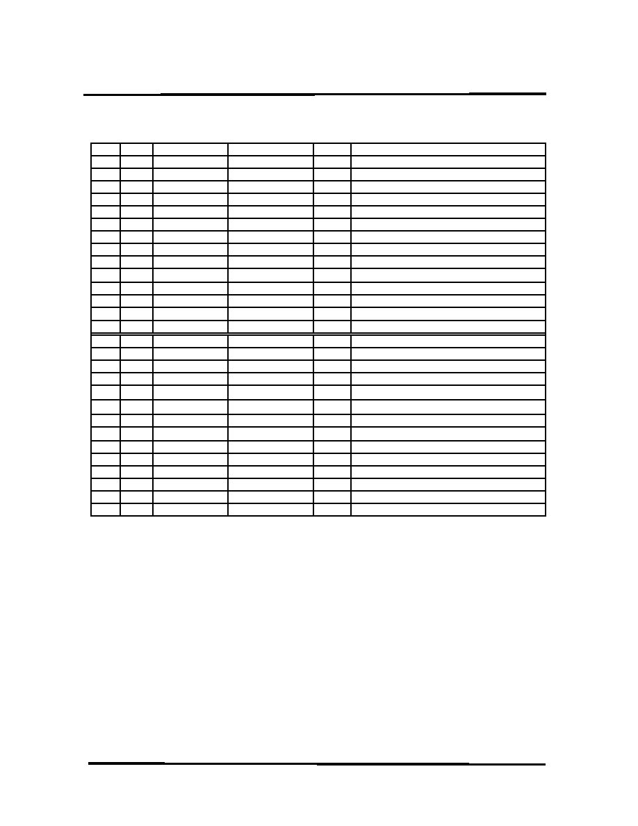
3.Pin description
Table 3.1 Pin descriptions
No.
I/O
Symbol
LEVEL
Logic Functionality
01
SVCC
-
+3.3V
02
GND
-
Ground
03
I
IDATAN
LV-PECL
N
Data input (neg.)
04
I
IDATAP
LV-PECL
P
Data input (pos.)
05
GND
GND
-
Ground
06
I
ICLKP
LV-PECL
P
Clock input (pos.)
07
I
ICLKN
LV-PECL
N
Clock input (neg.)
08
GND
-
Ground
09
I
SHUT
VCC or GND
-
LD shut down
10
O
TF
P
LD fail alarm (pos.)
11
O
TD
P
LD degrade alarm (pos.)
12
I
CLKSEL
VCC or GND
-
Tx clock select
13
GND
-
Ground
14
SVCC
-
+3.3V
15
RVCC
-
+3.3V
16
GND
-
Ground
17
I
ARESET
LV-TTL
-
Reset input for Limiter (neg.)
18
GND
-
Ground
19
GND
-
Ground
20
GND
-
Ground
21
GND
-
Ground
22
O
ODATAN
LV-PECL
N
Data output (neg.)
23
O
ODATAP
LV-PECL
P
Data output (pos.)
24
GND
-
Ground
25
GND
-
Ground
26
GND
-
Ground
27
GND
-
Ground
28
RVCC
-
+3.3V