
FSAN OLT Transceiver Preliminary
Specifications
Document NO: QPS-0202-090
Rev. DRAFT0.1
Oki Electric Industry Co., Ltd.
1/9
FSAN w/o OLT Transceiver
Specifications
Part Number : OAT6224S-OLT2-V4-A
Modification History
Rev.
Date
Originator
Comment
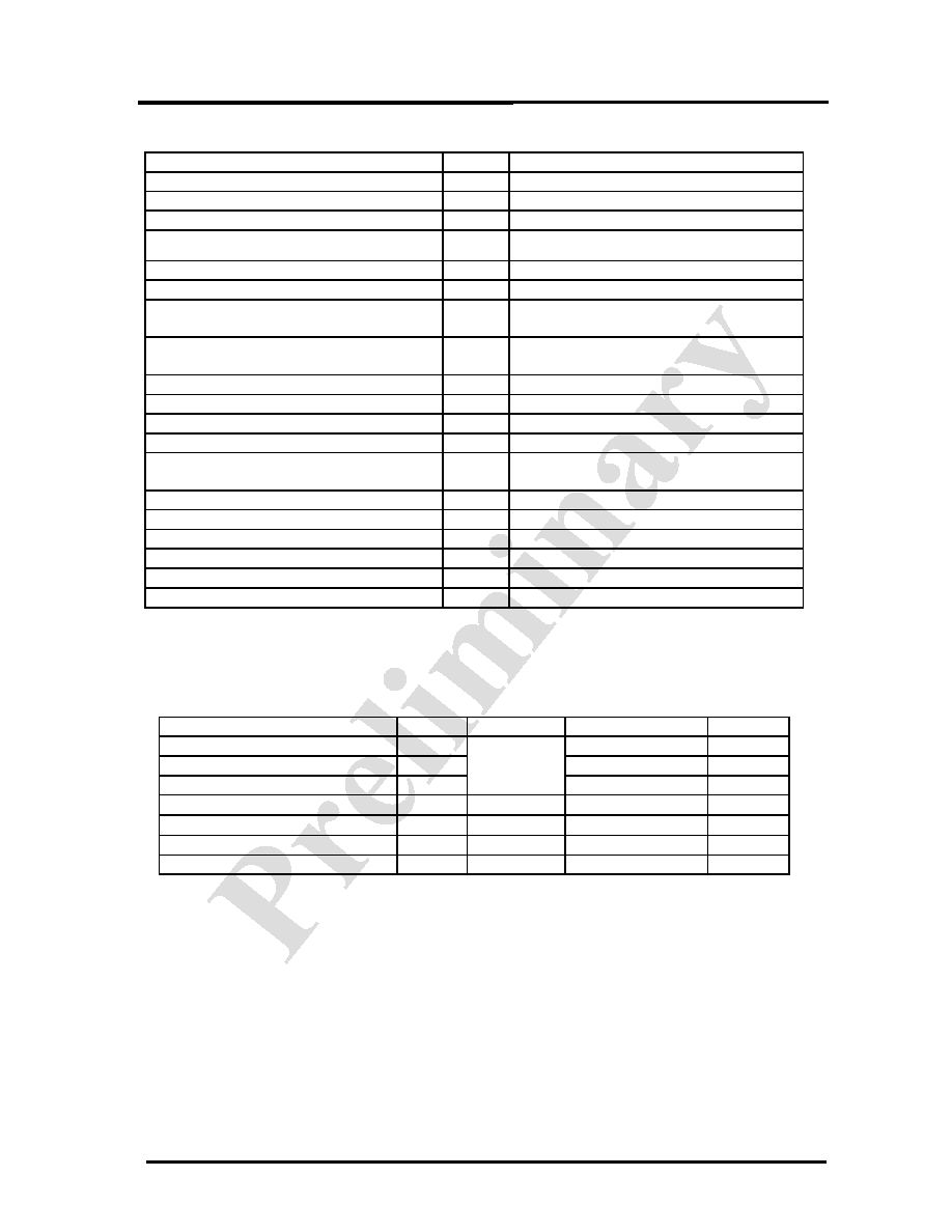
1. Specifications
Table 1.1 Specifications
Parameter
Unit
Specifications
Bit rate
Mbit/s
Tx:1244.16 / Rx:622.08
Transmission mode
-
Tx: continuous, Rx: burst
Transfer code
-
NRZ
Bi-directional transmission
-
1-fibre WDM
Transmission distance
km
20 (Max.)
Laser diode
-
1.49um DFB-LD
Photo detector
-
APD
Attenuation range
dB
5 - 20
Path penalty
dB
1
Operating temperature range
�
C
0 - 70
Operating humidity
%
5 - 95
Fiber/Connector type
-
Single mode fiber (10/125nm) / PC polished SC connector
Power supply voltage
V
+3.3 � 5%
Power consumption
W
2.0W (Typ.) , 2.5W (Max)
Dimension
mm
70 x 50 x 9.5
Document Number QPS-0202-090
Revision Draft0.1
DATE: Dec. 24, 2002
Author T.Tanaka
Project Manager K. YUSA
FSAN OLT Transceiver Preliminary
Specifications
Document NO: QPS-0202-090
Rev. DRAFT0.1
Oki Electric Industry Co., Ltd.
2/9
Table 1.2 Optical Characteristics (over operating temperature and lifetime)
Parameter
Unit
Specifications
Part number
OAT6224S-OLT2-V4-A
Operating wavelength
nm
Tx:1480 - 1500/Rx:1260 -1360
Mask of the transmitter eye diagram
Figure1.1
Maximum reflectance of equipment, measured at
transmitter wavelength
dB
-
Mean launched power range
dBm
-4.0 ~ +2.0
Minimum extinction ratio
dB
10
Tolerance to the transmitter incident light
power
dB
more than -15
Launched optical power
w/o input to the transmitter
dBm
-
Maximum spectral width
nm
1.0 (@-20dB)
Side mode suppression ratio
dB
More than 30
Jitter transfer
dB
-
Jitter generation in 1.3kHz bandwidth
UIpp
-
Maximum reflectance of equipment,
measured at receiver wavelength
dB
-
Bit error ratio
-
less than 10
-10
Minimum sensitivity
dBm
-27.0
Minimum overload
dBm
-6.0(Note)
Consecutive identical digit immunity
bit
more than 72
Jitter tolerance
-
-
Tolerance to the reflected optical power
dB
less than 10
Note: A noise possibility appears at the back of each packets.
Note: Off level light of ONU module needs less than -25dBm.
Table 1.3 Absolute maximum ratings
Parameter
Symbol
Conditions
Ratings
Unit
Power supply voltage
Vcc
0 to +4.5
V
Input voltage
Vi
0 to Vcc
V
Maximum output current
Io
Ta = 25
�
C
30
mA
Storage temperature
Tstg
-40 to +85
�
C
Soldering temperature/time
Ta = 25
�
C
250/10
�
C/sec
Maximum tension of fiber
500
g
Minimum bending radius
30
mm

FSAN OLT Transceiver Preliminary
Specifications
Document NO: QPS-0202-090
Rev. DRAFT0.1
Oki Electric Industry Co., Ltd.
3/9
Figure1.1 Eye mask pattern for OAT6224-OLT2
Table1.4 DC characteristic
Parameter
Unit
OAT6224-OLT2
MIN
TYP
MAX
PECL input high voltage
VCC-1.17
-
VCC-0.88
PECL input low voltage
VCC-1.81
-
VCC-1.47
PECL output high voltage
VCC-1.02
-
VCC-0.88
PECL output low voltage
VCC-1.81
-
VCC-1.62
LVTTL input high voltage
2.0
-
VCC+0.3
LVTTL input low voltage
-0.3
-
0.8
LVTTL output high voltage
2.4
-
Vcc
LVTTL output low voltage
V
GND
-
0.4
Clock input duty
%
40
50
60
Data output rise/fall time ( 20
- 80 % )
ns
2.5
Clock/Data input setup &
hold time
-
Figure4.1
Reset input timing
-
Figure4.2
Required preamble pattern
-
10101010
1.2
A
m
pl
i
t
ude
UI
0.20
0
0.5
1
0.28
0
-0.20
0.80
0.40
0.60
0.72
1
Mean level of logical 1
Mean level of logical 0

FSAN OLT Transceiver Preliminary
Specifications
Document NO: QPS-0202-090
Rev. DRAFT0.1
Oki Electric Industry Co., Ltd.
4/9
2.
Block diagram
Fig. 2.1 Block diagram
APD
LD
PD
LD Driver
APC
TF
1310nm
OPT I/O
1310nm/1490nm
WDM
DATA IN
SHUT IN
ATC
Pre-amp
1490nm
DATA OUT
CLK IN
TD
Shutdown
RESET IN
CLKSEL

FSAN OLT Transceiver Preliminary
Specifications
Document NO: QPS-0202-090
Rev. DRAFT0.1
Oki Electric Industry Co., Ltd.
5/9
3. Pin description
Table 3.1 Pin descriptions
No.
I/O
Symbol
LEVEL
Logic
Functionality
01
SVCC
-
+3.3V
02
GND
-
Ground
03
I
IDATAN
LV-PECL
N
Data input (neg.)
04
I
IDATAP
LV-PECL
P
Data input (pos.)
05
GND
GND
-
Ground
06
I
ICLKP
LV-PECL
P
Clock input (pos.)
07
I
ICLKN
LV-PECL
N
Clock input (neg.)
08
GND
-
Ground
09
I
SHUT
VCC or GND
-
LD shut down
10
O
TF
LV-TTL
P
LD fail alarm (pos.)
11
O
TD
LV-TTL
P
LD degrade alarm (pos.)
12
I
CLKSEL
VCC or GND
-
Tx clock select
13
GND
-
Ground
14
SVCC
-
+3.3V
15
RVCC
-
+3.3V
16
GND
-
Ground
17
I
ARESET
LV-TTL
-
Reset input for Limiter (neg.)
18
GND
-
Ground
19
GND
-
Ground
20
GND
-
Ground
21
GND
-
Ground
22
O
ODATAN
LV-PECL
N
Data output (neg.)
23
O
ODATAP
LV-PECL
P
Data output (pos.)
24
GND
-
Ground
25
GND
-
Ground
26
GND
-
Ground
27
GND
-
Ground
28
RVCC
-
+3.3V

FSAN OLT Transceiver Preliminary
Specifications
Document NO: QPS-0202-090
Rev. DRAFT0.1
Oki Electric Industry Co., Ltd.
6/9
4.
Timing condition
4.1 Data/Clock input timing
SDATAP/N
1.25Gbps
SCLKP/N
1.25GHz
t
clk
=800ps
t
su
t
H
t
su
>100ps
t
H
>100ps
Figure4.1 Data/Clock input setup & hold time (In case of using clock)
Note: If you don't use clock, you must terminate the clock input, that is, ICLKP=1.6V, ICLKN=2.4V.
4.2 Reset input timing
Electrical
output
Preceding cell
Preamble
GT>=8bits@622.08Mbps
t
rpw1
>=2bit@622.08bps
T
1
=<500ns@
(Note2)
T
2
>=2bits@622.08Mbps
t
rpw1
ARESETP/N
T
1
T
2
GT
Reset noise
(Note1)
Note1: Reset noise appears in electrical output. User must mask in this part. The range of this noise is
about 2bits the front and the rear of reset signal.
Note2: After packet cell, user must input ARESET. Because it is possible to output noise after packet cell
Figure4.2 Reset input timing

FSAN OLT Transceiver Preliminary
Specifications
Document NO: QPS-0202-090
Rev. DRAFT0.1
Oki Electric Industry Co., Ltd.
7/9
5.
Typical Application Circuit
IDATAP 04
IDATAN 03
*
*
ICLKP 06
ICLKN 07
*
*
LV-PECL
INPUT
SHUT 09
LV-TTL
INPUT
CLKSEL 12
VCC:Data is clocked
GND:Data is not clocked
ARESET 17
LV-TTL
INPUT
ODATAP
23
ODATAN
22
*
*
11 TD
1.6kohm
LV-TTL
OUTPUT
LV-PECL
OUTPUT
10 TF
1.6kohm
LV-TTL
OUTPUT
SVCC 01,14
RVCC 15,28
0.1uF
0.1uF
OAT6224S-OLT2-V4-A
02,05,08,
13,16,18,
19,20,21,
24,25,26,
27 GND
*
130ohm
82ohm
Thevenin
termination
SVCC
RVCC
RVCC
SVCC
22uF
22uF
22uH
22uH
+3.3V
Fig 5.1 Typical application circuit
FSAN OLT Transceiver Preliminary
Specifications
Document NO: QPS-0202-090
Rev. DRAFT0.1
Oki Electric Industry Co., Ltd.
8/9
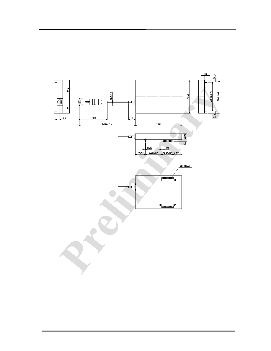
6. Outline
Fig 6.1 Package Outline

FSAN OLT Transceiver Preliminary
Specifications
Document NO: QPS-0202-090
Rev. DRAFT0.1
Oki Electric Industry Co., Ltd.
9/9
7. Precautions for handling
The circuits of these modules operate at very small signal. In order to avoid the degradation of the
optical sensitivity due to external noise, the bottom pattern of these modules on the PCB should be ground
pattern with low impedance.
Do not mount/pattern device/circuits which generate high frequency noise close to the module.
In order to operate the module stable against the power noise, install the power supply noise reduction
circuits.
The impedance between the power and ground pattern of the power circuit should be as low as possible.
The elements around the module should be mounted close to the pins of the module.
If an optical power exceeding the absolute maximum ratings is fed to the module, the optical receiver may
be damaged. Set the optical input power appropriately when in use of these modules.
8. Qualification and Reliability
To help ensure high product reliability and customer satisfaction, OKI is committed to an intensive quality
program that starts in the design phase and proceeds through the manufacturing process.
Optical transceiver modules are qualified to OKI internal standards using MIL-STD-883 test methods and
procedures and using sample techniques consistent with Telcordia requirements.
This qualification program fully meets the intent of Telcordia reliability practices GR-468-CORE.
9. Laser Safety
All version of transceiver are Class 1 Laser products FDA complies with 21 CFR 1040.10 and 1040.11
requirements.
Also, all versions are Class 1 Laser products pre IEC 825-1.