 | –≠–ª–µ–∫—Ç—Ä–æ–Ω–Ω—ã–π –∫–æ–º–ø–æ–Ω–µ–Ω—Ç: Z550 | –°–∫–∞—á–∞—Ç—å:  PDF PDF  ZIP ZIP |
Document Outline
- CD-ROM MAIN MENU
- ASIC Product Families
- Technical Documentation
- QA and Packaging
- Oki Corporate Information
- Oki Website www.okisemi.com
- Z550 DATA SHEET BOOKMARKS
- Table of Contents
- Description
- Features
- Signal Descriptions
- Functional Description
- Baud Rates Generator
- Master Reset
- Programming
- FIFO Interrupt Mode Operation
- FIFO Polled Operation
- AC Characteristics
- RELATED TECHNICAL DOCUMENTS
- Data Sheets
- ASIC Product Overview
- MSM12R/13R/98R
- MSM30R/32R/92R
- 10S/Z0xx
- Phase-Locked Loop
- W712 Universal Serial Bus Controller
- Application Notes
- JTAG Boundary Scan
- Oki Floorplanner
- Technical Briefs
- W110 10/100 BASE-T
- W712 Universal Serial Bus Controller
- User's Manuals
- MSM12R/13R/98R
- MSM30R/32R/92R
- Line Cards

D
ATA
S
HEET
O K I A S I C P R O D U C T S
August 1996
Z550
0.5 µm UART
Mega Macrocell

s
s
≠≠≠≠≠≠≠≠≠≠≠≠≠≠≠≠≠≠≠≠≠≠≠≠≠≠≠≠≠≠≠≠≠≠≠≠≠≠≠≠≠≠≠≠≠≠≠≠≠≠≠≠≠≠≠≠≠≠≠≠≠≠≠≠≠≠≠≠≠≠≠≠≠≠≠≠≠≠≠≠≠≠≠≠≠≠≠≠≠≠≠
Oki Semiconductor
CONTENTS
Description ................................................................................................................................................................2
Features .....................................................................................................................................................................2
Signal Descriptions ..................................................................................................................................................5
Functional Description ............................................................................................................................................7
Registers ..............................................................................................................................................................7
Baud Rate Generator .......................................................................................................................................14
Master Reset .....................................................................................................................................................16
Programming ...................................................................................................................................................17
FIFO Interrupt Mode Operation ....................................................................................................................17
FIFO Polled Mode Operation ........................................................................................................................18
AC Characteristics .................................................................................................................................................19

1
Oki Semiconductor
Z550 UART
0.5µm Technology Mega Macrocell for Universal Asynchronous Receiver/Transmitter
DESCRIPTION
The Z550 UART Mega Macrocell is a featured library element in all of OKI's 0.5µm Sea of Gates and 0.5µm
Customer Structured Array families. The OKI implementation of the mega macrocell is fully compatible
with industry standard 16550 functions.
The Z550 UART Mega Macrocell is an Asynchronous Communication Element (ACE), functionally equiv-
alent to the industry standard 16550 with 16 byte FIFOs available on both the transmitter and receiver. It
serves as a serial I/O interface in microcomputer systems performing serial to parallel conversions on data
characters received from peripheral devices or modems and parallel to serial conversions on data charac-
ters transmitted by the CPU. In FIFO mode, the FIFOs are enabled allowing 16 bytes of data to be stored
during both transmit and receive operations. The receive FIFO also provides three bits per byte of error
data. The status of the ACE can be read at any time by the CPU. Available information includes the type
and condition of transfer operations being performed and error conditions involving parity, overrun,
framing or break interrupt. The ACE includes a built in baud rate generator with 18 programmable baud
rates.
FEATURES
This Mega Macrocell Data Sheet contains all necessary information to enable the user to design a circuit
using the Z550 functions for OKI's 0.5µm Sea of Gates and 0.5µm Customer Structured Array families.
Supported ASIC Families
Family Name
Family Type
MSM13R0000
Sea of Gates
MSM98R000
Customer Structured Array
∑Full double buffering
∑Full status reporting
∑16 byte receive and transmit FIFOs reduce CPU
interrupts
∑Independent control of transmit, receive, line
status data set interrupts and FIFOs
∑Modem control signals include: CTS, DCD,
DSR, DTR, RI, RTS
∑Programmable serial interface characteristics:
-5, 6, 7, or 8 bit characters
-odd, even, or no parity generation and detection
-1, 1.5, or 2 stop bits
∑Programmable Baud Rate Generator
(dc to 56k baud)
∑Unique OKI methodology for input timing
analysis
∑Tailored design flow and test procedure
alleviates user from test vector generation to
verify Z550 functionality
∑Specially developed software merges OKI test
vectors with the user's circuit

s
Z550 UART
s
≠≠≠≠≠≠≠≠≠≠≠≠≠≠≠≠≠≠≠≠≠≠≠≠≠≠≠≠≠≠≠≠≠≠≠≠≠≠≠≠≠≠≠≠≠≠≠≠≠≠≠≠≠≠≠≠≠≠≠≠≠≠≠≠≠≠≠≠≠≠≠≠≠≠≠≠≠≠≠≠≠≠
2
Oki Semiconductor
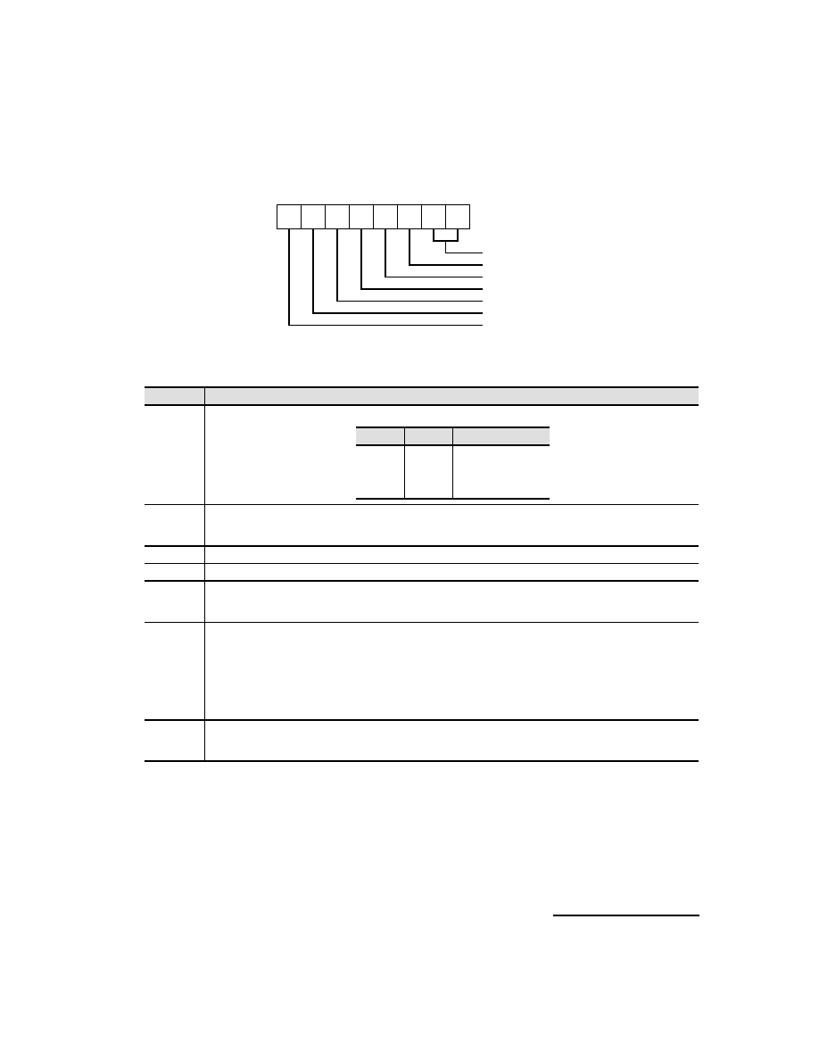
Figure 1. Logic Symbol
1.
Row/Column values (aspect ratio) include margin for layout overhead external to the mega macrocell for interconnection of input/output pins and
power buses.
Recommended Operating Conditions (V
SS
= 0 V)
Parameter
Symbol
Rated value
Units
Min
Typ
Max
Power supply voltage
V
DD
2.7
3.3
3.6
V
Operating temperature
T
j
-40
+25
+85
∞C
Mega Macrocell characteristics
Mega
Macrocell
Description
Logic
Gate
Count
Used Core Raw Gates
Number of Mega
Macrocell Pins
Number
of Core
Rows
[1]
Number of
Core Columns
[1]
Z550
Asynchronous Communication Element
5392
9519
(56.6%)
46
57
167
DO (0:7)
DI (0:7)
CS 0-1
A (0:2)
ADSN
DIS
DISN
DOS
DOSN
CLK
MR
CTS
OE
DDIS
DTR
RTS
OUT1
OUT2
SOUT
INTR
BAUD
DSR
RI
DCD
RCLK
SIN
TXRDY
RXRDY
CS2N

≠≠≠≠≠≠≠≠≠≠≠≠≠≠≠≠≠≠≠≠≠≠≠≠≠≠≠≠≠≠≠≠≠≠≠≠≠≠≠≠≠≠≠≠≠≠≠≠≠≠≠≠≠≠≠≠≠≠≠≠≠≠≠≠≠≠≠≠≠≠≠≠≠≠≠≠≠≠≠≠≠
s
Z550 UART
s
3
Oki Semiconductor
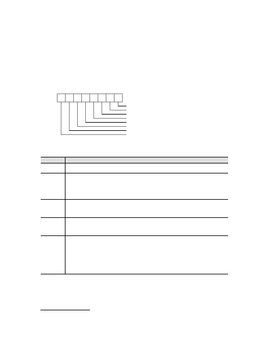
Figure 2. Block Diagram
DIS
DO 0-7
Control
Logic
RCLK
DISN
DOS
DOSN
ADSN
MR
CLK
OE
RXRDY
TXRDY
DDIS
CS0
CS1
CS2N
Chip Select
Logic
Data Buffer
DI 0-7
A0
A1
A2
Register
Select
Control
and Select
Logic
Interrupt
Logic
Transmitter
FIFO
Baud
Generator
Receiver
FIFO
Control
and Status
Register
Receiver
Shift
Register
Receiver
Control
and Timing
SIN
BAUD
Transmitter
Shift
Register
SOUT
INTR
RI
DCD
DSR
CTS
RTS
DTR
OUT2
OUT1
Modem
Control
Logic

s
Z550 UART
s
≠≠≠≠≠≠≠≠≠≠≠≠≠≠≠≠≠≠≠≠≠≠≠≠≠≠≠≠≠≠≠≠≠≠≠≠≠≠≠≠≠≠≠≠≠≠≠≠≠≠≠≠≠≠≠≠≠≠≠≠≠≠≠≠≠≠≠≠≠≠≠≠≠≠≠≠≠≠≠≠≠≠
4
Oki Semiconductor
SIGNAL DESCRIPTIONS
Signal Name
Type
Fan-In
Fan-Out
Max
Signal Description
DI 0-7
I
1
-
Data Input. Data Inputs 0-7 are used to transfer data and control information from the exter-
nal system to the ACE. DI0 is the first data bit to be transferred.
CS 0-1, 2N
I
1
-
Chip Select. The device is selected when CS0 and CS1 are high and CS2N is low.
A 0-2
I
1
-
Address. Address Lines 0-2 select the internal registers.
ADSN
I
1.6
-
Address Strobe. The state of the Chip Select and Address Lines are latched when ADSN is
low.
DIS
I
1
-
Read Strobe. Data transfers from the ACE to the output data bus when DIS is high.
DISN
I
1
-
Read Strobe. Same as DIS but active low.
DOS
I
1
-
Write Strobe. Data transfers from the input data bus to the ACE when DIS is high.
DOSN
I
1
-
Write Strobe. Same as DOS but active low.
CLK
I
1
-
Clock. Input for external timing reference.
MR
I
1
-
Master Reset. A high level resets the device, forcing the ACE into an idle state and suspends
all data activity until programmed to resume. The MCR and its output is cleared. The LSR is
cleared except for the THRE and TEMT bits, which are both sets.
CTS
I
1
-
Clear To Send . The state of CTS can be read from bit 4 (CTS) of the MSR. Bit 0 (DCTS) of the
MSR is set if the CTS input changes state since the last time the MSR was read. CTS low in-
dicates to the ACE that data on SOUT can be transmitted.
DSR
I
1
-
Data Send Ready. The state of DSR can be read from bit 5 (DSR) of the MSR. Bit 1 (DDSR)
of the MSR is set if the DSR input changes state since the last time the MSR was read. DSR
low indicates to the ACE that there is data ready for it to receive.
RI
I
1
-
Ring Indicator. A low signal indicates that a telephone ringing signal has been received by
the modem. The state of RI can be read from bit 6 (RI) of the MSR. Bit 2 (TERI) of the MSR
is set if the RI input changes from high to low since the last time the MSR was read.
DCD
I
1
-
Data Carrier Detect. The DCD signal indicates that the data carrier has been detected by the
modem. The state of DCD can be read from bit 7 (DCD) of the MSR. Bit 3 (DDCD) of the MSR
is set if the DCD input changed state since the last time the MSR is read.
RCLK
I
5
-
Receive Clock. This signal is an external input to the ACE's receiver logic (it is 16X the SIN
data rate).
SIN
I
2.5
-
Serial Input. The Serial Input receives serial data from the modem or other serial data source
into the ACE.
DO 0-4
DO5
DO6-7
O
-
16
19
16
Data Output. Data Outputs 0-7 are used to transfer data and status information from the ACE
to your system. DI0 is the first data bit to be received.
OE
O
-
40
Output Enable. This signal is a 3-state control used to configure the LSI pins of the ASIC for
production testing.
DDIS
O
-
15
Driver Disable . The macrocell asserts this signal LOW while the system is reading data from
the ACE.
DTR
O
-
16
Data Terminal Ready. The macrocell sets this signal LOW when a logic 1 has bene written
to bit 0 (DTR) of the MCR. This signal is set high when a logic 0 is written to bit 0 of the MCR
or whenever a reset occurs. A low DTR indicates that the ACE is ready to receive data.
RTS
O
-
16
Request To Send. This signal is set low by writing a logic 1 to bit 1 of the MCR. It is set high
when a logic 0 is written to bit 1 of the MCR or whenever a reset occurs. A low RTS signal
indicates that the ACE has data ready to transmit.

≠≠≠≠≠≠≠≠≠≠≠≠≠≠≠≠≠≠≠≠≠≠≠≠≠≠≠≠≠≠≠≠≠≠≠≠≠≠≠≠≠≠≠≠≠≠≠≠≠≠≠≠≠≠≠≠≠≠≠≠≠≠≠≠≠≠≠≠≠≠≠≠≠≠≠≠≠≠≠≠≠
s
Z550 UART
s
5
Oki Semiconductor
OUT1
O
-
16
Output 1. This output is set low by writing a logic 1 to bit 2 of the MCR, and set high by writing
a logic 0 to bit 2 of the MCR.
OUT2
O
-
16
Output 2. This output is set low by writing a logic 1 to bit 3 of the MCR, and set high by writing
a logic 0 to bit 3 of the MCR.
SOUT
O
-
19
Serial Data Out. This output is the serial data output of the ACE's transmitter circuitry.
INTR
O
-
18
Interrupt. The Interrupt output goes high whenever a Transmitter Holding Register Empty,
Received Data Available, Receiver Error Flag, Modem Status condition or Trigger Charge Tim-
eout (in FIFO mode) is detected and it is enabled in the IER.
BAUD
O
-
15
Baud Rate Out. This signal is the output of the internal Baud Rate Generator.
TXRDY
O
-
19
Transmit Ready . this signal provides two types of DMA signaling selected by bit 3 of the FCR
when operating with the FIFO's enabled.
In mode 0 (bit 3 of the FCR = 0), TXRDY will be active (= 0) when the XMIT FIFO and XMIT
holding register contain no characters. TXRDY will go high when the first character is loaded
into the holding register of the XMIT FIFO. This mode is normally used for single transfer DMA
operation.
In mode 1 (bit 3 of the FCR = 1), TXRDY will be active (=0) when there are no characters in
the XMIT FIFO. TXRDY will go high when the XMIT FIFO is completely full. This mode is nor-
mally used when continual multiple transfers, that fill the FIFO, are made.
NOTE: If the FIFO's are disabled (FIFO mode 0) only single DMA transfers are allowed.
RXRDY
O
-
19
Receiver Ready. this signal provides two types of DMA signaling selected by bit 3 of the FCR
when operating with the FIFO's enabled.
In mode 0 (bit 3 of the FCR = 0), RXRDY will be active (=0) when the RCVR FIFO and RCVR
holding register contain at least one characters. RXRDY will go high when there are no more
characters in the FIFO or holding register. This mode is normally used for single transfer DMA
operation.
In mode 1 (bit 3 of the FCR = 1), RXRDY will be active (=0) when the timeout or trigger levels
are reached. RXRDY will go high when the FIFO or holding register is empty. This mode is
normally used when continual multiple transfers, that fill the FIFO, are made.
NOTE: If the FIFO's are disabled (FIFO mode 0) only single DMA transfers are allowed.
SIGNAL DESCRIPTIONS (CONTINUED)
Signal Name
Type
Fan-In
Fan-Out
Max
Signal Description

s
Z550 UART
s
≠≠≠≠≠≠≠≠≠≠≠≠≠≠≠≠≠≠≠≠≠≠≠≠≠≠≠≠≠≠≠≠≠≠≠≠≠≠≠≠≠≠≠≠≠≠≠≠≠≠≠≠≠≠≠≠≠≠≠≠≠≠≠≠≠≠≠≠≠≠≠≠≠≠≠≠≠≠≠≠≠≠
6
Oki Semiconductor
FUNCTIONAL DESCRIPTION
Registers
Three types of internal registers are used in the ACE. The three types are the Control, Status, and Data
registers. The control registers are the Bit Rate Select Register DLL (Divisor Latch LSB) and DLM (Divisor
Latch MSB), Line Control Register, Interrupt Enable Register, and the Modem Control Registers. The sta-
tus registers are the Line Status Registers and the Modem Status Register. The data registers are the
Receiver Buffer Register and the Transmitter Holding Register. The Address, Read, and Write inputs are
used in conjunction with the Divisor Latch Access Bit in the Line Control Register [LCR(7)] to select the
register to be written or read (see the table below). Individual bits within these registers are referred to by
the register mnemonic and the bit number in parenthesis. As an example, LCR(7) refers to Line Control
Register Bit 7.
Transmitter Buffer Register and Receiver Buffer Register
The Transmitter Buffer Register and Receiver Buffer Register are data registers that hold from five to eight
bits of data. If less than eight data bits are transmitted, data is right justified to the LSB. Bit 0 of a data word
is always the first serial data bit received and transmitted. The ACE data registers are double-buffered so
that read and write operations may be performed when the UART is performing the parallel-to-serial or
serial-to-parallel conversion.
Line Control Register
The format of the data character is controlled by the Line Control Register. The contents of the LCR may
be read, eliminating the need for separate storage of the line characteristics in system memory. The con-
tents of the LCR is shown in Figure 3 and described in the following table.
1.
X = "Don't Care", 0 = Logic Low, 1 = Logic High.
2.
The serial channel is accessed when ≠CS0 is low.
Serial Channel Internal Register
[1]
[2]
DLAB
A2
A1
A0
Mnemonic
Register
0
0
0
X
X
X
X
X
X
1
1
0
0
0
0
0
1
1
1
1
0
0
0
0
0
1
1
0
0
1
1
0
0
0
0
1
0
1
0
1
0
1
0
1
RBR
THR
IER
IIR
LCR
MCR
LSR
MSR
SCR
DDL
DLM
Receiver Buffer Register (read only)
Transmitter Holding Register (write only)
Interrupt Enable Register
Interrupt Identification Register (read only)
Line Control Register
Modem Control Register
Line Status Register
Modem Status Register
Scratch Register
Divisor Latch (LSB)
Divisor Latch (MSB)
≠≠≠≠≠≠≠≠≠≠≠≠≠≠≠≠≠≠≠≠≠≠≠≠≠≠≠≠≠≠≠≠≠≠≠≠≠≠≠≠≠≠≠≠≠≠≠≠≠≠≠≠≠≠≠≠≠≠≠≠≠≠≠≠≠≠≠≠≠≠≠≠≠≠≠≠≠≠≠≠≠
s
Z550 UART
s
7
Oki Semiconductor
Figure 3. Line Control Register
Line Control Register Description
LCR Bit(s)
Description
LCR(0) and
LCR(1)
Word length select bits. The number of bits in each serial character is programmed as shown below.
LCR(2)
Stop Bit Select. LCR(2) specifies the number of stop bits in each transmitted character. If LCR(2) is a logic "0", one stop bit is gen-
erated. If LCR(2) is a logic "1" when a 5 bit word length is selected, 1.5 stop bits are generated. If LCR(2) is a logic "1" when either
a 6, 7, or 8 bit word length is selected, two stop bits are generated. The receiver checks for two stop bits if programmed to do so.
LCR(3)
Parity Enable. When LCR(3) is high, a parity bit between the last data word bit and stop bit is generated and checked.
LCR(4)
Even Parity Select. When parity is enabled [LCR(3) = 1], LCR(4) = 0 selects odd parity, and LCR(4) = 1 selects even parity.
LCR(5)
Stick Parity. When parity is enabled [LCR(3) = 1], CLR(5) = 1 causes the transmission and reception of a parity bit to be in the oppose
state from that indicated by LCR(4). This allows parity to be forced to a known state and the receiver to check the parity bit in a known
state.
LCR(6)
Break Control. When LCR(6) is set to a logic "1", the serial output (SOUT) is forced to the spacing (logic "0") state. The break is
disabled by setting LCR(6) to a logic "0". The Break Control bit acts only on SOUT and has no effect on the transmitter logic. Break
Control enables the CPU to alert a terminal in a computer communications system. If the following sequence is used, no invalid char-
acters will be transmitted because of the break.
∑ Load all "0"s (pad character) in response to THRE.
∑ Set the break in response to the next THRE.
∑ Wait for the transmitter to be idle (TEMT = 1), then clear the break when normal transmission is restored.
LCR(7)
Divisor Latch Access Bit (DLAB). LCR(7) must be set high (logic "1") to access the Divisor Latches DLL and DLM of the Baud Rate
Generator during read or write operations. LCR(7) must be set low (logic "0") to access the Receiver Buffer, the Transmitter Holding,
or the interrupt Enable Registers.
LCR
7
LCR
6
LCR
5
LCR
4
LCR
3
LCR
2
LCR
1
LCR
0
Word Length Select
Stop Bit Select
Parity Enable
Even Parity Select
Stick Parity
Break Control
Divisor Latch Access Bit
LCR(1)
LCR(0)
Word Length
0
0
1
1
0
1
0
1
5 data bits
6 data bits
7 data bits
8 data bits
s
Z550 UART
s
≠≠≠≠≠≠≠≠≠≠≠≠≠≠≠≠≠≠≠≠≠≠≠≠≠≠≠≠≠≠≠≠≠≠≠≠≠≠≠≠≠≠≠≠≠≠≠≠≠≠≠≠≠≠≠≠≠≠≠≠≠≠≠≠≠≠≠≠≠≠≠≠≠≠≠≠≠≠≠≠≠≠
8
Oki Semiconductor
Line Status Register
The Line Status Register (LSR) is a single register that provides status indications. The LSR is usually the
first register read by the CPU to determine the cause of an interrupt or to poll the status the serial channel.
The contents of the LSR is shown in Figure 4 and described in the following table.
Figure 4. Line Status Register
Line Status Register Description
LSR Bit(s)
Description
LSR(0)
Data Ready (DR). Data Ready is set high when an incoming character has been received and transferred into the Receiver Buffer
Register. LSR(0) is reset low by a CPU read of the data in the Receiver Buffer Register.
LSR(1)
Overrun Error (OE). Overrun Error indicates that data in the Receiver Buffer Register was not read by the CPU before the next
character was transferred into the Receiver Buffer Register, overwriting the previous character. The OE indicator is reset whenever
the CPU reads the contents of the Line Status Register.
An overrun error will occur in the FIFO Mode after the FIFO is full and the next character is completely received. The overrun error
is deleted by the CPU on the first LSR read after it happens. The character in the shift register is not transferred to the FIFO but it
is overwritten.
LSR(2)
Parity Error (PE). Parity Error indicates that the received data character does not have the correct parity, as selected by LCR(3)
and LCR(4). The PE bit is set high upon detection of a parity error, and is reset low when the CPU reads the contents of the LSR.
In the FIFO Mode, the Parity Error is associated with a particular character in the FIFO. LCR(2) indicates the error when the char-
acter is at the top of the FIFO.
LSR(3)
Framing Error (FE). Framing Error indicates that the received character did not have a valid stop bit. LSR(3) is set high when the
stop bit following the last data bit or parity bit is detected to be a logic "0" (spacing level). The FE indicator is reset low when the
CPU reads the contents of the LSR. In the FIFO Mode, the Framing Error is associated with a particular character in the FIFO.
LCR(3) indicates the error when the character is at the top of the FIFO.
LSR(4)
Break Interrupt (BI). Break Interrupt is set high when the received data input is held in the spacing (logic "0") state for a full word
transmission time (start bit + data bits + parity + stop bits). The BI indicator is reset when the CPU reads the contents of the Line
Status Register.
In the FIFO Mode, this is associated with a particular character in the FIFO. LCR(4) reflects the BI when the break character is at
the top of the FIFO. The error is deleted by the CPU when its associated character is at the top of the FIFO during the first LSR
read. Only one zero character is loaded into the FIFO when a BI occurs.
LSR(1)-LSR(4) are the error conditions that produce a Receiver Line Status interrupt [priority 1 interrupt in the Interrupt Identifi-
cation Register (IIR)] when any of the conditions are detected. This interrupt is enabled by setting IER(2)=1 in the Interrupt Enable
Register.
LSR
7
LSR
6
LSR
5
LSR
4
LSR
3
LSR
2
LSR
1
LSR
0
Overrun Error (OE) (Error=1, No Error=0)
Parity Error (PE) (Error=1, No Error=0)
Framing Error (FE) (Error=1, No Error=0)
Break Interrupt (BI) (Break=1, No Break=0)
Transmitter Holding Register Empty (THRE) (Empty=1, Not Empty=0)
Transmitter Empty (TEMT) (Empty=1, Not Empty=0)
Receiver FIFO Error (Error in FIFO=1, No Error in FIFO=0)
Data Ready (DR) (Ready=1, Not Ready=0)

≠≠≠≠≠≠≠≠≠≠≠≠≠≠≠≠≠≠≠≠≠≠≠≠≠≠≠≠≠≠≠≠≠≠≠≠≠≠≠≠≠≠≠≠≠≠≠≠≠≠≠≠≠≠≠≠≠≠≠≠≠≠≠≠≠≠≠≠≠≠≠≠≠≠≠≠≠≠≠≠≠
s
Z550 UART
s
9
Oki Semiconductor
FIFO Control Register
The FIFO Control Register is a write only register at the same location as the IIR. It is used to enable and
clear the FIFOs, set the trigger level of the RCVR FIFO, and select the type of DMA signaling.
Figure 5. FIFO Control Register
LSR(5)
THRE indicates that the ACE is ready to accept a new character for transmission. The THRE bit is set high when a character is
transferred from the Transmitter Holding Roister into the Transmitter Shift Register. LSR(5) is reset low by the loading of the
Transmitter Holding Register by the CPU. LSR(5) is not reset by a CPU read of the LSR. In FIFO Mode, when the XMlT FIFO is
empty, this bit is set. It is cleared when one byte is written to the XMlT Fife.
When the THRE interrupt is enabled IER(1), THRE causes a priority 3 interrupt in the IIR. If THRE is the interrupt source indicated
in IIR, lNTR is cleared by a read of the IIR.
LSR(6)
Transmitter Empty (TEMT). TEMT is set high when the Transmitter Holding Register (THR) and the Transmitter Shift Register
(TSR) are both empty. LSR(6) is reset low when a character is loaded into the THR and remains low until the character is trans-
ferred out of SOUT. TEMT is not reset low by a CPU read of the LSR. In the FIFO Mode, when both the transmitter FIFO and shift
register are empty, this bit is set to one.
LSR(7)
This bit is always 0 in the Z450 Mode. In FIFO Mode, it is set when at least one of the following data errors is in the FIFO: Parity
Error, Framing Error or Break Interrupt indication.
FIFO Control Register Description
FCR Bit(s)
Description
FCR(0)
FIFO ENABLE. Enables both the XMlT and RCVR FIFOs. Programming of other FCR bits is enabled by setting FCR(0)=1. The FIFOs
operate in Z450 mode when FCR(0)=0. All bytes in both FIFOs can be cleared automatically from the FIFOs when changing from
FIFO mode to Z450 mode and vice versa.
FCR(1)
RCVR FIFO Reset. This bit clears all bytes in the RCVR FIFO and resets the counter logic to 0 when it is set to a one. It does not
clear the receive shift register.
FCR(2)
XMlT FIFO Reset. This bit clears all bytes in the XMlT FIFO and resets the counter logic to 0 when it is set to a one. This does not
clear the transmit shift register.
Line Status Register Description (Continued)
LSR Bit(s)
Description
FCR
7
FCR
6
FCR
5
FCR
4
FCR
3
FCR
2
FCR
1
FCR
0
Receiver FIFO Reset (Reset Rx FIFO = 1)
Transmit FIFO Reset (Reset Tx FIFO = 1)
DMA Mode Select (DMA Mode 1 = 1, DMA Mode 0 = 0)
Not Used
Receiver FIFO Interrupt Trigger Level
FIFO Enable (FIFO Enable = 1)

s
Z550 UART
s
≠≠≠≠≠≠≠≠≠≠≠≠≠≠≠≠≠≠≠≠≠≠≠≠≠≠≠≠≠≠≠≠≠≠≠≠≠≠≠≠≠≠≠≠≠≠≠≠≠≠≠≠≠≠≠≠≠≠≠≠≠≠≠≠≠≠≠≠≠≠≠≠≠≠≠≠≠≠≠≠≠≠
10
Oki Semiconductor
Modem Control Register
The Modem Control Register (MCR) controls the interface with a modem or data set as shown in Figure 6
and the following table. The MCR can be written and read. The RTS and DTR outputs are directly con-
trolled by bits in this register. A high input asserts a low (true) at the output pins.
Figure 6. Modem Control Register
FCR(3)
DMA Mode Select. This bit controls the method of DMA signaling that will be used. If FCR(3)=1, the part will operate in Mode 1.
It will be in Mode 0 if FCR(3)=0. These modes are only valid if FCR(0)=1. It directly affects the operation of the RXRDY and TXRDY
outputs.
FCR(4)-FCR(5)
These bits are not used.
FCR(6)-FCR(7)
Rx FIFO Interrupt Trigger Level. These two bits are used to set the trigger level for the RCVR FIFO interrupt.
Modem Control Register Description
MCR Bit(s)
Bit Description
MCR(0):
When MCR(0) is set high, the DTR output is forced low. When MCR(0) is reset low, the DTR output is forced high.
MCR(1):
When MCR(1) is set high, the RTS output is forced low. When MCR(1) is reset low, the RTS output is forced high.
MCR(2):
When MCR(2) is set high, the OUT1 output is forced low. When MCR(2) is reset low, the OUT1 output is forced high.
MCR(3):
When MCR(3) is set high, the OUT2 output is forced low. When MCR(3) is reset low, the OUT2 output is forced high.
MCR(4):
MCR(4) provides a local loop back feature for diagnostic testing. When MCR(4) is set high, Serial Output (SOUT) is
set to the marking (logic "1") state. The receiver data input, Serial Input (SIN) is disconnected and the output of the
Transmitter Shift Register is looped back into the Receiver Shift Register input. The four modem control inputs (CTS,
DSR, DCD, and RI) are disconnected. The four MCR bits DTR, RTS, OUT1, and OUT2 are internally connected to
MSR(5), MSR(4), MSR(6), and MSR(7) in that order. The modem control output pins are forced to their inactive
state (high).
In the diagnostic mode, data transmitted is immediately received. This allows the processor to verify the transmit
and receive data paths of the selected serial channel.
Interrupt control is fully operational. However, interrupts are generated by controlling the lower four MCR bits inter-
nally. Interrupts are not generated by activity on the external pins represented by those four bus.
Bits MCR(5) - MCR(7):
Permanently set to logic "0".
FIFO Control Register Description (Continued)
FCR Bit(s)
Description
FCR (7)
FCR (6)
Rx FIFO Trigger Level
(Bytes)
0
0
1
1
0
1
0
1
01
04
08
14
MCR
7
MCR
6
MCR
5
MCR
4
MCR
3
MCR
2
MCR
1
MCR
0
(RTS) Request to Send (Output High=0, Output Low=1)
(Out1) Output1 (Output1 Set High=0, Output1 Set Low=1)
(Out2) Output1 (Output2 Set High=0, Output2 Set Low=1)
(LOOP) Loopback Function (Disabled=0, Enabled=1)
Bit is set to "0"
Bit is set to "0"
Bit is set to "0"
(DTR) Data Terminal Ready (Output High=0, Output Low=1)

≠≠≠≠≠≠≠≠≠≠≠≠≠≠≠≠≠≠≠≠≠≠≠≠≠≠≠≠≠≠≠≠≠≠≠≠≠≠≠≠≠≠≠≠≠≠≠≠≠≠≠≠≠≠≠≠≠≠≠≠≠≠≠≠≠≠≠≠≠≠≠≠≠≠≠≠≠≠≠≠≠
s
Z550 UART
s
11
Oki Semiconductor
Modem Status Register
The Modem Status Register (MSR) provides the CPU with status of the modem input lines from modems
or peripheral devices. The MSR allows the CPU to read the serial channel modem signal inputs by access-
ing the data bus interface of the ACE. In addition to the current status information, four bits of the MSR
indicate whether the modem inputs have changed since the last reading of the MSR. The delta status bus
are set high when a control input from the modem changes state, and reset low when the CPU reads the
MSR.
The modem input lines are CTS, DSR, RI, and DCD. MSR(4) - MSR(7) are status indications of these lines.
A status bit = 1 indicates the input is a low. A status bit = 0 indicates the input is high. If the modem status
interrupt in the Interrupt Enable Register is enabled [IER(3)=1] an interrupt is generated whenever
MSR(0)-MSR(3) is set to a one. The MSR is a priority 4 interrupt. The contents of the Modem Status Reg-
ister are described in Figure 7 and the following table.
Figure 7. Modem Status Register
Reading the MSR Register will clear the delta modem status indications but has no effect on the other sta-
tus bits.
Modem Status Register Description
MSR Bit
Description
MSR(0)
Delta Clear to Send (DCTS): DCTS indicates that the CTS input to the serial channel has changed state since the last time it was read by
the CPU
MSR(1)
Delta Data Set Ready (DDSR): DDSR indicates that the DSR input to the serial channel has changed state since the last time it was read
by the CPU.
MSR(2)
Trailing Edge of Ring Indicator (TERI): TERI indicates that the RI input to the serial channel has changed state from high to low since the
last time it was read by the CPU. Low to high transitions on RI do not activate TERI.
MSR(3)
Delta Data Carrier Detect (DDCD): DDCD indicates that the DCD input to the serial channel has changed state since the last time it was
read by the CPU.
MSR(4)
Clear to Send (CTS): CTS is the complement of the CTS input from the modem indicating to the serial channel that the modem is ready
to receive data from the serial channel's transmitter output (SOUT). If the serial channel is in loop mode [MSR(4) = 1], MSR(4) is equiv-
alent to the RTS value in the MCR.
MSR(5)
Data Set Ready (DSR): Data Set Ready (DSR) is the compliment of the DSR input from the modem to the serial channel which indicates
that the modem is ready to provide data to the serial channel receiver circuitry. If the channel is in the loop mode [MCR(4) = 1], MSR(5)
is equivalent to the DTR value in the MCR.
MSR(6)
Ring indicator (RI): is the compliment of the RI input. If the channel is in the loop mode [MCR(4) = 1], MSR(6) is equivalent to the OUT1
value in the MCR.
MSR(7)
MSR(7) Data Carrier Detect (DCD): Data Carrier Detect indicates the compliment of the Data Carrier Detect (DCD) input. If the channel
is in the loop mode [MCR(4) = 1], MSR(7) is equivalent to OUT2 value in the MCR.
MSR
7
MSR
6
MSR
5
MSR
4
MSR
3
MSR
2
MSR
1
MSR
0
(DDSR) Delta Data Set Ready
(TERI) Trailing Edge of Ring Indicator
(DDCD) Delta Data Carrier Detect
(CTS) Clear to Send
(DSR) Data Set Ready
(RI) Ring Indicator
(RLSD) Receiver Line Signal Detect
(DCTS) Delta Clear to Send

s
Z550 UART
s
≠≠≠≠≠≠≠≠≠≠≠≠≠≠≠≠≠≠≠≠≠≠≠≠≠≠≠≠≠≠≠≠≠≠≠≠≠≠≠≠≠≠≠≠≠≠≠≠≠≠≠≠≠≠≠≠≠≠≠≠≠≠≠≠≠≠≠≠≠≠≠≠≠≠≠≠≠≠≠≠≠≠
12
Oki Semiconductor
For LSR and MSR, the setting of status bits is inhibited during status register read operations. If a status
condition is generated during a read operation, the status bit is not set until the trailing edge of the read.
If a status bit is set during a read operation, and the same status condition occurs, that status bit will be
cleared at the trailing edge of the read instead of being set again.
Scratchpad Register
The Scratchpad Register is an 8-bit, Read/ Write register that has no effect on either channel in the ACE.
It is intended to be used by the programmer for temporarily data storage.
Interrupt Identification Register
The Interrupt Identification Register (IIR) in the serial channel of the ACE provides interrupt interfacing
capability. To minimize software overhead, the serial channel prioritizes interrupts into four levels. The
four levels of interrupt conditions are:
Information indicating that a prioritized interrupt is pending and the type of interrupt is stored in the
Interrupt Identification Register (IIR). When addressed during chip select time, the IIR indicates the high-
est priority interrupt pending. No other interrupts are acknowledged until that interrupt is serviced by
the CPU. The contents of the IIR is shown in the following tables.
Interrupt Priorities
Interrupt Condition
Priority
Receiver Line Status
1
Received Data Ready
2
Transmitter Holding Register Empty
3
Modem Status
4
Interrupt Identification Register Bits
IIR Bit(s)
Bit Description
IIR(0)
When IIR(0) is low, an interrupt is pending. When IIR(0) is high, no interrupt is pending.
IIR(1) and IIR(2)
These two bits are used to identify the highest priority interrupt pending as indicated in the following table.
IIR(3)
This bit is always logic "0" in Z450 Mode. In FIFO Mode, this bit is set along with IIR(2) when a timeout interrupt is pending.
IIR(4) and IIR(5)
These bits of the IIR are always logic "0".
IIR(6) and IIR(7)
FRC(0)=1 sets these bits to logic "1".

≠≠≠≠≠≠≠≠≠≠≠≠≠≠≠≠≠≠≠≠≠≠≠≠≠≠≠≠≠≠≠≠≠≠≠≠≠≠≠≠≠≠≠≠≠≠≠≠≠≠≠≠≠≠≠≠≠≠≠≠≠≠≠≠≠≠≠≠≠≠≠≠≠≠≠≠≠≠≠≠≠
s
Z550 UART
s
13
Oki Semiconductor
Interrupt Enable Register
The Interrupt Enable Register (IER) is used to independently enable the four serial channel interrupts
which activate the interrupt (INTR) output. All interrupts are disabled by resetting IER(0) - IER(3) of the
Interrupt Enable Register to a logic "0". Interrupts are enabled by setting the appropriate bits of the IER
high. Disabling the interrupt system inhibits the Interrupt Identification Register and the INTR output. All
other system functions operate in their normal manner, including the setting of the Line Status and
Modem Status Registers. The contents of the Interrupt Enable Register is described in the following table. .
Baud Rate Generator
The ACE serial channel contains a programmable Baud Rate Generator (BRG) that divides the clock (DC
to 3.1 MHz) by any divisor from 1 to 216-1. The output of the Baud Rate Generator is referred to as RCLK.
The frequency of RCLK 16x the data rate. The desired divisor is calculated by the following equation:
[divisor = clock ˜ (baud rate x 16)]. Two 8-bit divisor latch registers store the divisor in a 16-bit binary for-
mat. These Divisor Latch registers must be loaded during initialization. Upon loading ether of the Divisor
Latches, a 16-bit baud counter is immediately loaded. This prevents long counts on initial load. Setting
1.
The exact time will be [(word length) x 7 - 2] x 8 + [(trigger level - number of characters) x 8 + 1] RCLKs.
Interrupt Identification (IIR) Register Description
FIFO
Mode
Only
Interrupt Identification
Interrupt Set and Reset Functions
Bit 3
Bit 2
Bit 1
Bit 0
Priority
Level
Interrupt Flag
Interrupt Source
Interrupt Reset Control
0
0
0
1
-
None
None
≠
0
1
1
0
First
Receiver Line Status
OE, PE, FE, or BI
LSR Read
0
1
0
0
Second
Received Data Available
Receiver data available for 450 or 550
mode, or trigger level reached for
FIFO mode
RBR read or FIFO drops below
the trigger level
1
1
0
0
Second
Trigger Change Level
Indication
Minimum of one character in the
RCVR FIFO and no character input or
removed during a time period
depending on how many characters
are in FIFO and what the trigger level
is set at (3.5 to 4.5 character
times
[1]
).
RBR read
0
0
1
0
Third
THRE
THRE
Read of IIR or THR write
0
0
0
0
Fourth
Modem Status
CTS, DSR, RI, or DCD
MSR read
Interrupt Enable Register Bits
IER Bit(s)
Bit Description
IER(0):
When programmed high (IER(0) = Logic "1"), ERBFI enables the Received Data Available Interrupt.
IER(1):
When programmed high (IER(1) = Logic "1"), ETBEI enables the Transmitter Holding Register Empty Interrupt.
IER(2):
When programmed high (IER(2) = Logic "1"), ELSI enables the Receiver Line Status Interrupt.
IER(3):
When programmed high (IER(3) = Logic "1"), EDSSI enables the Modem Status Interrupt.
IER(4) - IER(7):
These four bits of the IER are logic "0".
s
Z550 UART
s
≠≠≠≠≠≠≠≠≠≠≠≠≠≠≠≠≠≠≠≠≠≠≠≠≠≠≠≠≠≠≠≠≠≠≠≠≠≠≠≠≠≠≠≠≠≠≠≠≠≠≠≠≠≠≠≠≠≠≠≠≠≠≠≠≠≠≠≠≠≠≠≠≠≠≠≠≠≠≠≠≠≠
14
Oki Semiconductor
DLL = 1 and DLM = 0 selects a divisor = 1 (dividing by 1 gives maximum baud rate for a given input fre-
quency at the CLK input).
The BRG can use any of four different popular frequencies to provide standard baud rates. These frequen-
cies are 1.8432 MHz, 2.4576 MHz, 3.072 MHz, and 8 MHz. The following tables illustrate the divisors
needed to obtain standard bit rates from 50 to 256k bps using these three clock frequencies.
BAUD Rates (1.8432 MHz Clock)
Desired BAUD Rate
Divisor Used
Percent Error Difference Between
Desired and Actual
50
75
110
134.5
150
300
600
1200
1800
2000
2400
3600
4800
7200
9600
19200
38400
56000
2304
1536
1047
857
768
384
192
96
64
58
48
32
24
16
12
6
3
2
-
-
0.026
0.058
-
-
-
-
-
0.69
-
-
-
-
-
-
-
2.86
BAUD Rates (2.4576 MHz Clock)
Desired BAUD Rate
Divisor Used
Percent Error Difference Between
Desired and Actual
50
75
110
134.5
150
300
600
1200
1800
2000
2400
3600
4800
7200
9600
19200
38400
3072
2048
1396
1142
1024
512
256
128
85
77
64
43
32
21
16
8
4
-
-
0.026
0.0007
-
-
-
-
0.392
0.260
+
0.775
-
1.587
-
-
-

≠≠≠≠≠≠≠≠≠≠≠≠≠≠≠≠≠≠≠≠≠≠≠≠≠≠≠≠≠≠≠≠≠≠≠≠≠≠≠≠≠≠≠≠≠≠≠≠≠≠≠≠≠≠≠≠≠≠≠≠≠≠≠≠≠≠≠≠≠≠≠≠≠≠≠≠≠≠≠≠≠
s
Z550 UART
s
15
Oki Semiconductor
Master Reset
After power up, the ACE MR input should be held high to reset the ACE to an idle mode. A high, logic
"1", on MR causes the following:
1.Initializes the transmitter and receiver internal clock counters.
BAUD Rates (3.072 MHz Clock)
Desired BAUD Rate
Divisor Used
Percent Error Difference Between
Desired and Actual
50
75
110
134.5
150
300
600
1200
1800
2000
2400
3600
4800
7200
9600
19200
38400
3840
2560
1745
1428
1280
640
320
160
107
96
80
53
40
27
20
10
5
-
-
0.026
0.034
-
-
-
-
0.312
-
-
0.628
-
1.23
-
-
-
BAUD Rates (8 MHz Clock)
Desired BAUD Rate
Divisor Used to
Generate 16x Clock
Percent Error Difference Between
Desired and Actual
50
75
110
134.5
150
300
600
1200
1800
2000
2400
3600
4800
7200
9600
19200
38400
56000
128000
256000
1000
6667
4545
3717
3333
1667
833
417
277
250
208
139
104
69
52
26
13
9
4
2
≠
0.005
0.010
0.013
0.010
0.020
0.040
0.080
0.080
≠
0.160
0.080
0.160
0.644
0.160
0.160
0.160
0.790
2.344
2.344

s
Z550 UART
s
≠≠≠≠≠≠≠≠≠≠≠≠≠≠≠≠≠≠≠≠≠≠≠≠≠≠≠≠≠≠≠≠≠≠≠≠≠≠≠≠≠≠≠≠≠≠≠≠≠≠≠≠≠≠≠≠≠≠≠≠≠≠≠≠≠≠≠≠≠≠≠≠≠≠≠≠≠≠≠≠≠≠
16
Oki Semiconductor
2.Clears the Line Status Register (LSR), except for Transmitter Shift Register Empty (TEMT) and Trans-
mit Holding Register Empty (THRE), which are set. When interrupts are subsequently enabled, an
interrupt occurs due to THRE. The Modem Control Register (MCR) is also cleared. All of the discrete
lines, memory elements and miscellaneous logic associated with these register bits are also cleared or
turned off. The Line Control Register (LCR), Divisor Latches, Receiver Buffer Register, and Transmit-
ter Buffer Register are not effected.
A summary of the effect of a reset on the ACE is given in the table below.
Following removal of the reset condition (MR low), the ACE remains in the idle mode until programmed.
If rclk is connected to the baudout signal, then while loading DLL and DLM registers, X's appear on baud-
out pins and propagate through to the LSR register. Subsequent reads of this LSR register cause X's to
appear on the data bus.
The following solutions can solve the above problem.
∑At the very beginning of simulation, until data is written into the DLL and DLM registers, hold rclk
to a known value (either "1" or "0"). The rclk input can be connected to baudout after writing data to
these registers. During real chip operation, the "1" or "0" value eventually propagates into the LSR
register, so this is not a design problem. Unknown states are created during simulation because
there is a feedback loop in the Z550 latch connection, and unknown states stay in latches
permanently once they have propagated there.
∑Instead of connecting baudout to rclk, leave these two signals altogether unconnected. Additional
external circuitry is then required to drive the receiver clock, rclk.
∑Reset the UART; write "1" to bit 7 of the LCR register; write any data into DDL and DLM; and
perform another reset. This procedure should not have any problems, although you will also have to
write new data into the DDL and DLM registers.
Master Reset
Register/Signal
Reset Control
Reset
Interrupt Enable Register
Reset
All bits low (0-3 forced and 4-7 permanent)
Interrupt Identification Register
Reset
Bit 0 is high, Bits 1 and 2 low, Bits 3-7 are permanently low.
Line Control Register
Reset
All bits low.
MODEM Control Register
Reset
All bits low.
Line Status Register
Reset
All bits low, except bits 5 and 6.
MODEM Status Register
Reset
Bits 0-3 low, Bits 4-7 input signal.
SOUT
Reset
High
Interrupt (RCVR Errs)
Read LSR/Reset
Low
Interrupt (RCVR Data Ready)
Read RBR/Reset
Low
Interrupt (THRE)
Read IIR/Write THR/Reset
Low
Interrupt (Modem Status Changes)
Read MSR/Reset
Low
Out 2
Reset
High
RTS
Reset
High
DTR
Reset
High
Out 1
Reset
High

≠≠≠≠≠≠≠≠≠≠≠≠≠≠≠≠≠≠≠≠≠≠≠≠≠≠≠≠≠≠≠≠≠≠≠≠≠≠≠≠≠≠≠≠≠≠≠≠≠≠≠≠≠≠≠≠≠≠≠≠≠≠≠≠≠≠≠≠≠≠≠≠≠≠≠≠≠≠≠≠≠
s
Z550 UART
s
17
Oki Semiconductor
Programming
The serial channel of the ACE is programmed by the control registers; LCR, IER, DLL and DLM, and MCR.
These control words define the character length, number of stop bits, parity, baud rate, and modem inter-
face.
While the control registers can be written to in any order, the IER should be written to last because it con-
trols the interrupt enables. Once the serial channel is programmed and operational, these registers can be
updated any time the serial channel is not transmitting or receiving data.
FIFO Interrupt Mode Operation
The following RCVR interrupts will occur when the RCVR FIFO and receive interrupts are enabled. All
interrupts reflect the byte at the top of the FIFO. The interrupt descriptions are in order of decreasing
priority.1.IIR=01 indicates that there are no interrupts pending.
2.IIR=06 (Receive Line Status Interrupt) indicates that the byte at the top of the FIFO has some sort of
error in it (OE, PE, FE, or BI). This interrupt is cleared by reading the LSR. Reading the LSR will also
indicate which one of the errors is in that byte.
3.The IIR will equal an 04 when received data is available in the RCVR FIFO. In Mode 0, this occurs
when a complete character is transferred from the receiver shift register to the RCVR FIFO. In Mode
1, the RCVR FIFO must be filled at or above the trigger level with data. This interrupt is cleared by
reading the data f from the RBR, until it either is empty (Mode 0) or the amount of data in it is less
than the trigger level (Mode 1). LSR(0)=1 indicates that the data in the top byte in the RCVR FIFO is
available, When the FIFO is emptied by reading the Receive Buffer Register, LSR(0) is reset to a zero.
The Trigger Level Change interrupt (IIR = 0C) description is found in the following section. It has the
same priority as the Receiver Data Available interrupt (IIR = 04).
A.If the following conditions exist, a FIFO trigger change level interrupt will occur.
∑Minimum of one character in FIFO.
∑Last received serial character was longer than 3.5 to 4.5 continuous previous character times (if
two stop lets are programmed, the second one is included in the time delay) Once 3.5 character
times have been met and no accesses have been made to the FIFO, the trigger level matches the
number of FIFO characters and the trigger change level interrupt will be returned to its original
programmed value.
∑The last CPU read of the FIFO was more than 3.5 to 4.5 continuous character times ago. At 300
baud with 12 bit characters, the FIFO timeout interrupt causes a latency of 160ms maximum,
from received character to interrupt issued.
B.By using the RCLK input for a clock signal, the character times can be calculated. (The delay is
proportional to the baud rate.)
C.The trigger change level timer is reset after the CPU reads the RCVR FIFO or after a new character
is received when there has been no trigger change level interrupt.
D.A trigger change level interrupt is cleared and the timer is reset when the CPU reads a character
from the RCVR FIFO.

s
Z550 UART
s
≠≠≠≠≠≠≠≠≠≠≠≠≠≠≠≠≠≠≠≠≠≠≠≠≠≠≠≠≠≠≠≠≠≠≠≠≠≠≠≠≠≠≠≠≠≠≠≠≠≠≠≠≠≠≠≠≠≠≠≠≠≠≠≠≠≠≠≠≠≠≠≠≠≠≠≠≠≠≠≠≠≠
18
Oki Semiconductor
4.IIR=02 (THRE interrupt) indicates that the Transmit Holding Register is empty. This interrupt is
cleared by ether writing a byte to the THR or by reading the IIR.
5.IIR=00 (Modem Status interrupt) indicates that there has been some change in the status of the
modem. This interrupt is cleared by reading the MSR, will also indicate what type of status change
occurred.
XMIT interrupts will occur as follows when the transmitter and XMIT FIFO interrupts are enabled
(FCR(0)=l, IER(l)=l)
1.The XMIT FIFO empty indications will be delayed one character time minus the last stop bit time
whenever THRE=1 and there have not been a minimum of two bytes at the same time in XMlT FIFO,
since the last THRE=1.
2.When the XMIT FIFO is empty, the transmitter holding register interrupt (IIR=02) occurs. The inter-
rupt is cleared as soon as the transmitter holding register is written to or the IIR is read.
When FCR(0) is enabled, an interrupt will not occur immediately even though it is enabled
(IER=1).The first XMIT interrupt occurs due to the conditions stated in 1 and 2 above only after data
has first been loaded into the XMIT FIFO.
XMIT FIFO empty interrupts have the same priority as RCVR FIFO trigger level and character trigger
change level interrupts.
FIFO Polled Mode Operation
Resetting IER(0), IER(l), IER(2), IER(3) all to zero, with FCR(0)=1, puts the ACE into the FIFO Polled Mode.
Since the RCVR and XMIT channels are controlled separately, ether or both can be operated in Polled
Mode.
In the FIFO Polled Mode, no timeout condition are indicated or trigger level reached. However, the RCVR
and XMIT FIFOs still have the capability of holding characters.

≠≠≠≠≠≠≠≠≠≠≠≠≠≠≠≠≠≠≠≠≠≠≠≠≠≠≠≠≠≠≠≠≠≠≠≠≠≠≠≠≠≠≠≠≠≠≠≠≠≠≠≠≠≠≠≠≠≠≠≠≠≠≠≠≠≠≠≠≠≠≠≠≠≠≠≠≠≠≠≠≠
s
Z550 UART
s
19
Oki Semiconductor
AC CHARACTERISTICS
1.
Typical condition is 3.3 V, T
j
= 25
∞
C for typical process.
2.
Applicable only when ADSN is tied low.
Z550 UART Input Timing (10 MHz @ 3.3V)
Parameter
Symbol
3.3 V (Typ)
[1]
Units
Address strobe width
t
ADS
5
ns
Address setup time
t
AS
11
ns
Address hold time
t
AH
0
ns
Chip select setup time
t
CS
12
ns
Chip select hold time
t
CH
0
ns
DIS/DISN Strobe Width
t
DIW
15
ns
Read Cycle Delay
t
RC
0
ns
Read Cycle = t
AR
[2]
+ t
DIW
+ t
RC
RC
24
ns
DOS/DOSN strobe width
t
DOW
11
ns
Write cycle delay
t
WC
4
ns
Write cycle = t
AW
+ t
DOW
+ t
WC
WC
25
ns
Data setup time
t
DS
8
ns
Data hold time
t
DH
5
ns
Address hold time from DIS/DISN
[2]
t
RA
0
ns
Chip select hold time from DIS/DISN
[2]
t
RCS
0
ns
DIS/DISN delay from address
[2]
t
AR
9
ns
DIS/DISN delay from chip select
[2]
t
CSR
0
ns
Address hold time from DOS/DOSN
[2]
t
WA
0
ns
Chip select hold time from DOS/DOSN
[2]
t
WCS
0
ns
DOS/DOSN delay from address
[2]
t
AW
10
ns
DOS/DOSN delay from select
[2]
t
CSW
0
ns
Master reset pulse width
t
MRW
15
ns
Duration of clock high pulse
t
XH
15
ns
Duration of clock low pulse
t
XL
7
ns

s
Z550 UART
s
≠≠≠≠≠≠≠≠≠≠≠≠≠≠≠≠≠≠≠≠≠≠≠≠≠≠≠≠≠≠≠≠≠≠≠≠≠≠≠≠≠≠≠≠≠≠≠≠≠≠≠≠≠≠≠≠≠≠≠≠≠≠≠≠≠≠≠≠≠≠≠≠≠≠≠≠≠≠≠≠≠≠
20
Oki Semiconductor
1.
Typical condition is 3.3 V, T
j
= 25
∞
C for typical process.
2.
Limited by DLL/DLM reg.
3.
f
X
= 8 MHz, divider value = 2.
4.
Maximum 2 µs.
5.
Maximum 1 RCLK cycle.
6.
Maximum 1µs.
Z550 UART Output Timing (10 MHz @ 3.3 V)
Parameter
Symbol
3 .3 V (Typ)
[1]
Units
DIS/DISN to drive disable delay
t
DD
1
ns
Delay from DIS/DISN to data
t
DDD
4
ns
DIS/DISN to floating data delay
t
HZ
2
ns
Delay from DOS/DOSN (WR THR) to reset interrupt
t
HR
6
ns
Delay from initial INTR reset interrupt
t
IRS
< 16
BAUDOUT
Delay from initial write to interrupt
t
SI
8 ~ 24
BAUDOUT
Delay from start bit low to interrupt (THRE) high
t
STI
8
BAUDOUT
Delay from DIS/DISN (RD IIR) to reset interrupt (THRE)
t
IR
4
ns
Delay from start to TXRDY active
t
SXA
< 8
BAUDOUT
Delay from write to TXRDY inactive
t
WXI
11
ns
Delay from DOS/DOSN (WR MCR) to output
t
MDO
4
ns
Delay to set interrupt from modem input
t
SIM
11
ns
Delay to reset interrupt for DIS/DISN (RS MSR)
t
RIM
4
ns
Baud divisor
N
[2]
ns
Baud output negative edge delay
t
BLD
3
ns
Baud output positive edge delay
t
BHD
3
ns
Baud output down time
t
LW
125
ns
[3]
Baud output up time
t
HW
125
ns
[3]
Delay from RCLK to sample time
t
SCD
[4]
µs
Delay from stop to set interrupt
t
SINT
[5]
RCLK
Delay from DIS/DISN (RD RBR/RDLSR) to reset interrupt
t
RINT
[6]
µs
≠≠≠≠≠≠≠≠≠≠≠≠≠≠≠≠≠≠≠≠≠≠≠≠≠≠≠≠≠≠≠≠≠≠≠≠≠≠≠≠≠≠≠≠≠≠≠≠≠≠≠≠≠≠≠≠≠≠≠≠≠≠≠≠≠≠≠≠≠≠≠≠≠≠≠≠≠≠≠≠≠
s
Z550 UART
s
21
Oki Semiconductor
Figure 8. Read Cycle
ADSN
t
ADS
A0, A1, A2
t
AH
t
AS
CS0, CS1,
CS2N
t
RA*
t
RCS
Valid
Valid
t
CS
t
CH
DOS/DOSN
t
CSR*
t
AR*
Active
Active
t
DIW
t
RC
RC
DIS/DISN
Active
OR
DI 0-7
t
HZ
t
DDD
Valid Data
DDIS
t
DS
t
DD
* Applicable only when ADSN is tied low.

s
Z550 UART
s
≠≠≠≠≠≠≠≠≠≠≠≠≠≠≠≠≠≠≠≠≠≠≠≠≠≠≠≠≠≠≠≠≠≠≠≠≠≠≠≠≠≠≠≠≠≠≠≠≠≠≠≠≠≠≠≠≠≠≠≠≠≠≠≠≠≠≠≠≠≠≠≠≠≠≠≠≠≠≠≠≠≠
22
Oki Semiconductor
Figure 9. Write Cycle Timing
Figure 10. Modem Timing
ADSN
t
ADS
A0, A1, A2
t
AH
t
AS
CS0, CS1,
CS2N
t
WA
t
WCS
Valid
Valid
t
CS
t
CH
DOS/DOSN
t
CSW
t
AW
Active
Active
t
DOW
t
WC
WC
DIS/DISN
Active
OR
DI 0-7
t
DH
t
DS
Valid Data
DOS/DOSN
(WR MCR)
(Note 1)
t
MDO
RTS, OTR,
OUT1, OUT2
CTS. DSR.
DCD
INTR
DISN
(RD MSR)
(Note 2)
RI
t
MDO
t
SIM
t
RIM
t
RIM
t
SIM
t
SIM
Note: 1. See WRITE timing diagram.
2. See READ timing diagram.

≠≠≠≠≠≠≠≠≠≠≠≠≠≠≠≠≠≠≠≠≠≠≠≠≠≠≠≠≠≠≠≠≠≠≠≠≠≠≠≠≠≠≠≠≠≠≠≠≠≠≠≠≠≠≠≠≠≠≠≠≠≠≠≠≠≠≠≠≠≠≠≠≠≠≠≠≠≠≠≠≠
s
Z550 UART
s
23
Oki Semiconductor
Figure 11. BAUD Out
Figure 12. Receiver Timing
CLK
BAUD (+1)
t
BHD
t
BLD
t
HW
N
t
LW
BAUD (+2)
t
BHD
t
BLD
t
HW
t
LW
BAUD (+3)
t
BLD
t
BHD
t
HW
t
LW
BAUD
(+N, N>3)
t
BLD
t
BHD
t
HW
t
HW
= (N-2) XTAL1 Cycles
SIN
(Receiver
Input Data)
t
SCD
INTR
(DATA Ready or
RCVR ERR)
RCLK
8 CLKs
SAMPLE CLK
SAMPLE CLK
Start
Data Bits (5-8)
Parity
Stop
DISN
t
SINT
Active
t
RINT
note 1
Z450 Mode

s
Z550 UART
s
≠≠≠≠≠≠≠≠≠≠≠≠≠≠≠≠≠≠≠≠≠≠≠≠≠≠≠≠≠≠≠≠≠≠≠≠≠≠≠≠≠≠≠≠≠≠≠≠≠≠≠≠≠≠≠≠≠≠≠≠≠≠≠≠≠≠≠≠≠≠≠≠≠≠≠≠≠≠≠≠≠≠
24
Oki Semiconductor
Figure 13. Receiver Ready - MODE 0
Figure 14. Receiver Ready - Mode 1
DIS/DISN
(RDRBR)
SIN
(First Byte)
SAMPLE CLK
Stop
t
SINT
(Note 1)
Active
t
RINT
Notes:1. If FCR0=1, then t
SINT
= 3 RCLKs. For a timeout interrupt, t
SINT
= 8 RCLKs.
RXRDY
DIS/DISN
(RDRBR)
SIN
(First Byte that
reaches the
trigger level)
SAMPLE CLK
Stop
t
SINT
(Note 2)
Active
t
RINT
Notes:1. This is the reading of the last byte in the FIFO.
2. If FCR0=1, then t
SINT
= 3 RCLKs. For a timeout interrupt, t
SINT
= 8 RCLKs.
RXRDY
(Note 1)

≠≠≠≠≠≠≠≠≠≠≠≠≠≠≠≠≠≠≠≠≠≠≠≠≠≠≠≠≠≠≠≠≠≠≠≠≠≠≠≠≠≠≠≠≠≠≠≠≠≠≠≠≠≠≠≠≠≠≠≠≠≠≠≠≠≠≠≠≠≠≠≠≠≠≠≠≠≠≠≠≠
s
Z550 UART
s
25
Oki Semiconductor
Figure 15. Transmitter Timing
Figure 16. Transmitter Ready - MODE 0
Figure 17. Transmitter Ready - MODE 1
DOSN
(WR THR)
(Note 1)
SERIAL OUT
(SOUT)
INTR
(THRE)
Start
Data Bits (5-8)
Parity
Stop
(1-2)
DISN
(RD IIR)
(Note 2)
Start
t
HR
t
HR
t
IR
t
IRS
t
STI
t
SI
Notes:1. This is the reading of the last byte in the FIFO.
2. If FCR0=1, then t
SINT
= 3 RCLKs. For a timeout interrupt, t
SINT
= 8 RCLKs.
TXRDY
SOUT
Data
Parity
Stop
Start
t
WXI
t
SXA
DOS/DOSN
(WRTHR)
Byte #1
TXRDY
SOUT
Data
Parity
Stop
Start
t
WXI
t
SXA
DOS/DOSN
(WRTHR)
FIFO Full
Byte #16

s
Z550 UART
s
≠≠≠≠≠≠≠≠≠≠≠≠≠≠≠≠≠≠≠≠≠≠≠≠≠≠≠≠≠≠≠≠≠≠≠≠≠≠≠≠≠≠≠≠≠≠≠≠≠≠≠≠≠≠≠≠≠≠≠≠≠≠≠≠≠≠≠≠≠≠≠≠≠≠≠≠≠≠≠≠≠≠
26
Oki Semiconductor
Figure 18. Receiver FIFO First Byte (This sets RDR)
Figure 19. Receiver FIFO Remaining Bytes
INTR
(Trigger Level
Interrupt)
(FCR6, 7=0, 0)
SAMPLE CLOCK
Data (5-8)
Stop Start
t
SINT
(Note 1)
SIN
INTR
(LSR Interrupt)
DISN
(RDLSR)
DISN
(RDRBR)
PAR
FIFO
Trigger Level
FIFO <
Trigger Level
t
RINT
t
RINT
Active
Active
INTR
(Timeout or
Trigger Level
Interrupt)
SAMPLE CLOCK
Data (5-8)
Stop Start
t
SINT
(Note 1)
SIN
INTR
(LSR Interrupt)
DISN
(RDLSR)
DISN
(RDRBR)
PAR
FIFO
Trigger Level
FIFO <
Trigger Level
t
RINT
t
RINT
Active
Active
Active
t
SINT
Top Byte of FIFO
Previous Byte
read from FIFO

Oki Semiconductor
The information contained herein can change without notice owing to product and/or technical improvements.
Please make sure before using the product that the information you are referring to is up-to-date.
The outline of action and examples of application circuits described herein have been chosen as an explanation of the standard action
and performance of the product. When you actually plan to use the product, please ensure that the outside conditions are reflected in
the actual circuit and assembly designs.
OKI assumes no responsibility or liability whatsoever for any failure or unusual or unexpected operation resulting from misuse, neglect,
improper installation, repair, alteration or accident, improper handling, or unusual physical or electrical stress including, but not limited
to, exposure to parameters outside the specified maximum ratings or operation outside the specified operating range.
Neither indemnity against nor license of a third party's industrial and intellectual property right,etc.is granted by us in connection with
the use of product and/or the information and drawings contained herein. No responsibility is assumed by us for any infringement of a
third party's right which may result from the use thereof.
When designing your product, please use our product below the specified maximum ratings and within the specified operating ranges,
including but not limited to operating voltage, power dissipation, and operating temperature.
The products listed in this document are intended for use in general electronics equipment for commercial applications (e.g.,office
automation, communication equipment, measurement equipment, consumer electronics, etc.).These products are not authorized for
use in any system or application that requires special or enhanced quality and reliability characteristics nor in any system or application
where the failure of such system or application may result in the loss or damage of property or death or injury to humans. Such
applications include, but are not limited to: traffic control, automotive, safety, aerospace, nuclear power control, and medical, including
life support and maintenance.
Certain parts in this document may need governmental approval before they can be exported to certain countries. The purchaser
assumes the responsibility of determining the legality of export of these parts and will take appropriate and necessary steps, at their
own expense, for export to another country.
Copyright 1995 OKI SEMICONDUCTOR
OKI Semiconductor reserves the right to make changes in specifications at anytime and without notice. This information furnished by
OKI Semiconductor in this publication is believed to be accurate and reliable. However, no responsibility is assumed by OKI
Semiconductor for its use; nor for any infringements of patents or other rights of third parties resulting from its use. No license is
granted under any patents or patent rights of OKI.

Northwest Area
785 N. Mary Avenue
Sunnyvale, CA 94086
Tel: 408/720-8940
Fax: 408/720-8965
Southwest Area
2302 Martin Street
Suite 250
Irvine, CA 92715
Tel: 714/752-1843
Fax: 714/752-2423
Central Area
2007 N. Collins Blvd.
Suite 303
Richardson, TX 75080
Tel: 214/690-6868
Fax: 214/690-8233
Southeast Area
1590 Adamson Parkway
Suite 220
Morrow, GA 30260
Tel: 404/960-9660
Fax: 404/960-9682
Eastern Area
Shattuck Office Center
138 River Road
Andover, MA 01810
Tel: 508/688-8687
Fax: 508/688-8896
Automotive Electronics
17177 N. Laurel Park Drive
Suite 433
Livonia, MI 48152
Tel: 313/464-7200
Fax: 313/464-1724
Oki R
EGIONAL
S
ALES
O
FFICES
Corporate Headquarters
785 N. Mary Avenue
Sunnyvale, CA 94086-2909
Tel: 408/720-1900
Fax: 408/720-1918
FOR OKI LITERATURE:
Call toll free 1-800-OKI-6388
(6 a.m. to 5 p.m. Pacific Time)
Oki Stock No:
OKIFAX SERVICE:
(800) OKI-6994
OKI WEB SITE:
http://www.okisemi.com
010708-001