Oxford Semiconductor Ltd.
69 Milton Park, Abingdon, Oxon, OX14 4RX, UK
Tel: +44 (0)1235 824900 Fax: +44(0)1235 821141
©
©
Oxford Semiconductor 1999
OXFW900 Data Sheet Revision 1.0 ≠ Nov 1999
Part No. OXFW900-TQ-A
F
EATURES
∑
S400 compliant 1394-1995 Link and Transaction
layers
∑
Compatible with 1394-1995 and 1394A Phys.
∑
Buffer Manager with max. RAM bandwidth of
800Mbps
∑
Microsoft Win98-Second Edition, Win2000 and Apple
MacOS 8.5 generic driver support
∑
SBP-2 Target Revision 4 compliant interface
∑
Fully ATA-4 compliant (see T13-1153D)
∑
Sustained IDE transfer rate of 25 Mbytes per second,
Peak transfer rate of 50Mbytes per second.
∑
Supports PIO modes 0 to 4, DMA modes 0 to 2 and
Ultra DMA modes 0 to 2
∑
Integrated 32-bit RISC processor (ARM7TDMI) with
on-chip scratch RAM
∑
ORB co-processor to accelerate translation of ORBs
to ATAPI commands
∑
Supports ORB chaining for increased performance
∑
High performance ATA command translation in
firmware using Reduced Block Command (RBC) set
∑
Optional External Serial ROM interface for
configuration data, user serial number, etc.
∑
Blank Flash memory programming feature via 1394
bus
∑
3.3 Volts operation
∑
Low Power CMOS
∑
Firmware and Flash Programming Utilities supplied by
Oxford Semiconductor
∑
ultra-thin 128-TQFP package (14mm x 14mm x 1mm )
D
ESCRIPTION
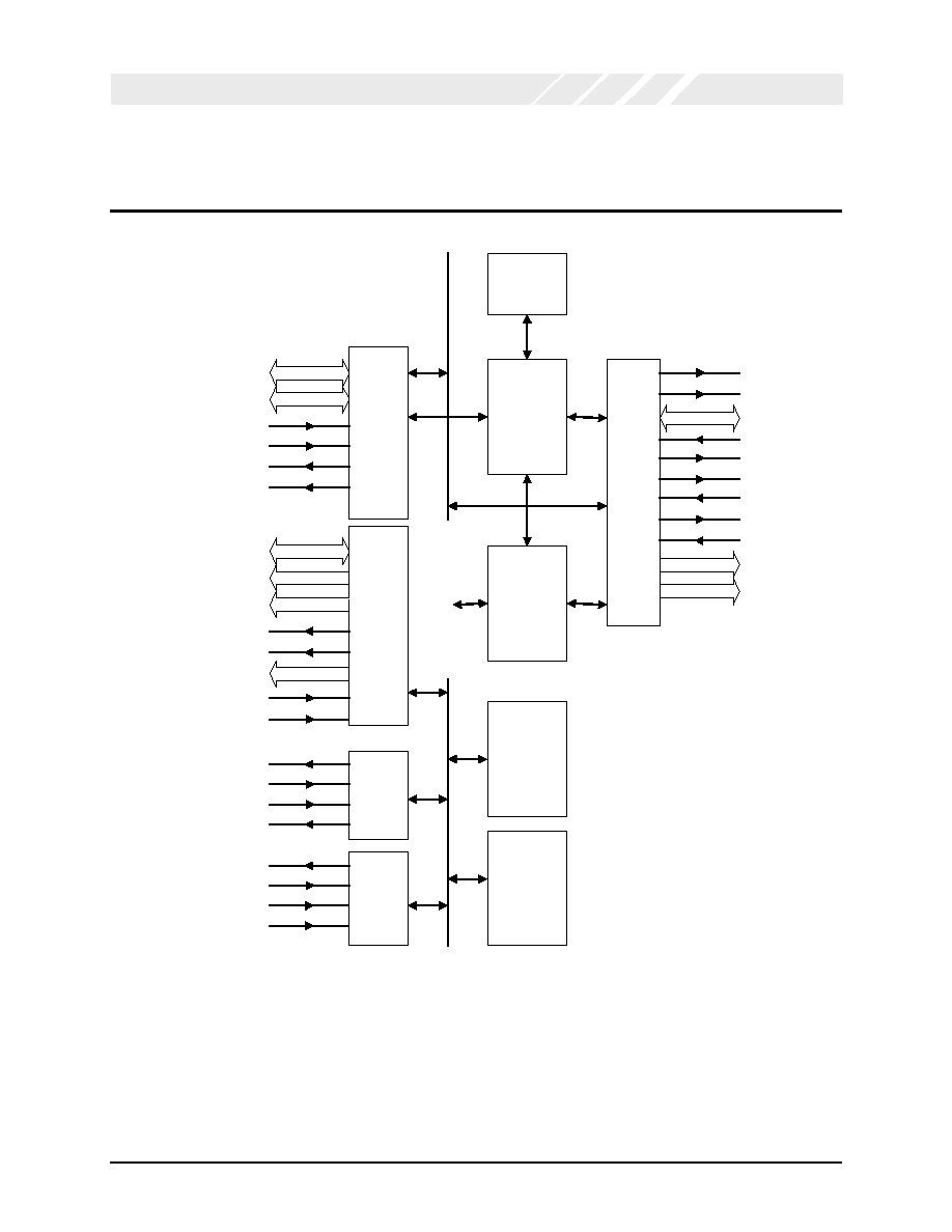
The OXFW900 is a high-performance 1394 to
ATA/ATAPI (IDE) native bridge with an integrated target
Serial Bus Protocol (SBP-2 ) controller. By supporting
the SBP-2 protocol, the device can use generic SBP-2
drivers available in the Microsoft Windows 98SE, Microsoft
Windows 2000, Microsoft Millennium and Apple MacOS
operating systems.
The device is ideally suited for smart-cable or tailgate
interface applications for removable-media drives, compact
flash card readers, CD-ROM, CD-R, CD-RW, DVD-ROM,
DVD-RAM and hard disk drives, allowing IDE drives to be
connected to a 1394 serial bus in a plug-and-play fashion.
Both ATA and ATAPI devices are supported using the
same firmware.
This highly integrated device offers a three-chip solution to
native bridge applications using an external 1394 PHY and
Flash ROM. A slow 32Kx8 Flash ROM (up to 120ns) is
sufficient for most optical media applications. For
applications that need a sustained data rate in excess of
10Mbytes per second, for example high performance disk
drives, an 8-bit 50ns FLASH or faster is recommended.
The device is compatible with both 1394-1995 and 1394A
PHYs.
The LINK controller complies with S400 1394-1995
specification. The 1394 transaction layer and SBP-2
protocol is implemented using a combination of the
ARM7TDMI (low-power 32-bit RISC processor), an ORB
(Operational Request Block) hardware co-processor and a
high performance buffer manager.
The Buffer Manager has a RAM bandwidth of 800Mbps. It
provides storage for 1394 and ATA/ATAPI packets,
automatically storing them and passing them to the
appropriate destinations, without any intervention from the
processor. It also provides storage and manages the
sequencing of ORB fetching to reduce latency and improve
data throughput.
The configuration data including the IEEE OUI
(Organisational Unique Identifier) and device serial number
is stored in the Flash ROM which may be uploaded from
the 1394 bus, even when blank. The device also facilitates
firmware uploads from the 1394 bus.
The ORB co-processor translates ORBs as defined in the
SBP-2 protocol into ATA/ATAPI commands, and
automatically stores error/status messages at an address
specified by the host.
Concurrent operation of the ATA/ATAPI and 1394
interfaces are facilitated using the high throughput Buffer
Manager where LINK, ATAPI manager and ARM7TDMI
can perform interleaved accesses to the on-chip RAM
buffer. The high performance processor ensures that no
significant latency is incurred. The ATA command
translation is performed in firmware to meet RBC (Reduced
Block Commands) standard, T10-1228D. The ATA/ATAPI
Manager supports PIO modes 0 to 4, DMA modes 0 to 2
and Ultra DMA mode 0 to 2 and provides the interface to
the IDE bus. It is compliant with T13-1153D, ATA-4
specification.
OXFW900
IEEE1394 to ATA/ATAPI Native Bridge
Data Sheet

Data Sheet Revision 1.0 Page 5
OXFW900
OXFORD SEMICONDUCTOR LTD.
3 P
IN
D
ESCRIPTIONS
1394 PHY-LINK interface
Dir
1
Name
Description
104, 105, 108, 109, 110, 111, 115,
116
I/O
PD[7:0]
Phy-Link Data Bus
117,118
I/O
CTL[1:0]
Phy-Link Control Bus
120
I
PHYCLK
49.152 MHz clock sourced by PHY
122
O
LREQ
Link Request
102
IU
LINKON
Requests link to power up when in a low power mode
103
O
LPS
Indicates to phy that link is powered and ready
ARM external interface
2, 3, 4, 5, 6, 7, 10, 11, 12, 13, 14,
15, 18, 19, 20, 21
T_I/O D[15:0]
ARM external data bus
35, 36, 37, 40, 41, 42, 43, 44, 45,
48, 49, 50, 51, 52, 53, 54, 60
T_O A[16:0]
ARM external address bus
25, 26, 29, 30
T_O CS#[3:0]
ARM external chip selects. CS0# is always used for program
ROM.
31
T_O OE#
ARM external output enable. Active when reading data from
external devices including program ROM
32, 33
T_O BWR#[1:0]
Byte Write enables. For future expansion
34
T_O WE#
Write Enable. Active when writing to external devices
62
ID
WIDTH16
`1' = 16 bit external ROM `0' = 8 bit external ROM
(pulldown)
61
T_IU INT#
External ARM interrupt
IDE interface
65, 66, 69, 70, 71, 72, 73, 74, 77,
78, 79, 80, 81, 82, 85, 86
T_I/O ID[15:0]
IDE data bus
97, 98, 99
T_O IA[2:0]
IDE address bus
100, 101
T_O ICS#[1:0]
IDE chip select. Selects IDE drive 0 or 1
63
T_O IDE_OE#[
IDE output enable. Only used when external buffering is
required to drive IDE data bus
64
T_O IRESET
IDE interface reset
89
T_I
DMARQ
90
T_O DIOW#
IDE interface write strobe
91
T_O DIOR#
IDE interface read strobe
92
T_O IORDY
95
T_O DMACK#
96
T_I
INTRQ
EEPROM interface
128
O
GPO3
General Purpose Output 3
126
O
GPO1
General Purpose Output 1
1
IU
GPI
General Purpose Input
127
O
GPO2
General Purpose Output 2
Miscellaneous Pins
57
I
XTLI
Crystal Oscillator input. 24.576 MHz crystal required. If a
clock module is used rather than a crystal then this input
must be tied high for the OXFW900 to operate, and the clock
module output connected to the CKIN pin. IMPORTANT -
See Application Notes regarding clocking
58
O
XTLO
Crystal Oscillator output. IMPORTANT ≠ See Application
Notes regarding clocking.