 | –≠–ª–µ–∫—Ç—Ä–æ–Ω–Ω—ã–π –∫–æ–º–ø–æ–Ω–µ–Ω—Ç: 2N5686 | –°–∫–∞—á–∞—Ç—å:  PDF PDF  ZIP ZIP |
High-Current Complementary
Silicon Power Transistors
. . . designed for use in high≠power amplifier and switching circuit
applications.
∑
High Current Capability ≠
I
C
Continuous = 50 Amperes.
∑
DC Current Gain ≠
h
FE
= 15≠60 @ I
C
= 25 Adc
∑
Low Collector≠Emitter Saturation Voltage ≠
V
CE(sat)
= 1.0 Vdc (Max) @ I
C
= 25 Adc
ŒŒŒŒŒŒŒŒŒŒŒŒŒŒŒŒŒŒŒŒŒŒŒ
ŒŒŒŒŒŒŒŒŒŒŒŒŒŒŒŒŒŒŒŒŒŒŒ
MAXIMUM RATINGS (1)
ŒŒŒŒŒŒŒŒŒŒŒ
ŒŒŒŒŒŒŒŒŒŒŒ
Rating
ŒŒŒŒŒ
ŒŒŒŒŒ
Symbol
ŒŒŒŒŒŒŒ
ŒŒŒŒŒŒŒ
2N5684
2N5686
ŒŒŒ
ŒŒŒ
Unit
ŒŒŒŒŒŒŒŒŒŒŒ
ŒŒŒŒŒŒŒŒŒŒŒ
Collector≠Emitter Voltage
ŒŒŒŒŒ
ŒŒŒŒŒ
V
CEO
ŒŒŒŒŒŒŒ
ŒŒŒŒŒŒŒ
80
ŒŒŒ
ŒŒŒ
Vdc
ŒŒŒŒŒŒŒŒŒŒŒ
ŒŒŒŒŒŒŒŒŒŒŒ
Collector≠Base Voltage
ŒŒŒŒŒ
ŒŒŒŒŒ
V
CB
ŒŒŒŒŒŒŒ
ŒŒŒŒŒŒŒ
80
ŒŒŒ
ŒŒŒ
Vdc
ŒŒŒŒŒŒŒŒŒŒŒ
ŒŒŒŒŒŒŒŒŒŒŒ
Emitter≠Base Voltage
ŒŒŒŒŒ
ŒŒŒŒŒ
V
EB
ŒŒŒŒŒŒŒ
ŒŒŒŒŒŒŒ
5.0
ŒŒŒ
ŒŒŒ
Vdc
ŒŒŒŒŒŒŒŒŒŒŒ
ŒŒŒŒŒŒŒŒŒŒŒ
Collector Current ≠ Continuous
ŒŒŒŒŒ
ŒŒŒŒŒ
I
C
ŒŒŒŒŒŒŒ
ŒŒŒŒŒŒŒ
50
ŒŒŒ
ŒŒŒ
Adc
ŒŒŒŒŒŒŒŒŒŒŒ
ŒŒŒŒŒŒŒŒŒŒŒ
Base Current
ŒŒŒŒŒ
ŒŒŒŒŒ
I
B
ŒŒŒŒŒŒŒ
ŒŒŒŒŒŒŒ
15
ŒŒŒ
ŒŒŒ
Adc
ŒŒŒŒŒŒŒŒŒŒŒ
Œ
ŒŒŒŒŒŒŒŒŒ
Œ
ŒŒŒŒŒŒŒŒŒŒŒ
Total Device Dissipation @ T
C
= 25
_
C
Derate above 25
_
C
ŒŒŒŒŒ
Œ
ŒŒŒ
Œ
ŒŒŒŒŒ
P
D
ŒŒŒŒŒŒŒ
Œ
ŒŒŒŒŒ
Œ
ŒŒŒŒŒŒŒ
300
1.715
ŒŒŒ
Œ
Œ
Œ
ŒŒŒ
Watts
W/
_
C
ŒŒŒŒŒŒŒŒŒŒŒ
Œ
ŒŒŒŒŒŒŒŒŒ
Œ
ŒŒŒŒŒŒŒŒŒŒŒ
Operating and Storage Junction
Temperature Range
ŒŒŒŒŒ
Œ
ŒŒŒ
Œ
ŒŒŒŒŒ
T
J
, T
stg
ŒŒŒŒŒŒŒ
Œ
ŒŒŒŒŒ
Œ
ŒŒŒŒŒŒŒ
≠65 to +200
ŒŒŒ
Œ
Œ
Œ
ŒŒŒ
_
C
ŒŒŒŒŒŒŒŒŒŒŒŒŒŒŒŒŒŒŒŒŒŒŒ
ŒŒŒŒŒŒŒŒŒŒŒŒŒŒŒŒŒŒŒŒŒŒŒ
THERMAL CHARACTERISTICS (1)
ŒŒŒŒŒŒŒŒŒŒŒŒ
ŒŒŒŒŒŒŒŒŒŒŒŒ
Characteristic
ŒŒŒŒŒ
ŒŒŒŒŒ
Symbol
ŒŒŒŒŒŒ
ŒŒŒŒŒŒ
Max
ŒŒŒ
ŒŒŒ
Unit
ŒŒŒŒŒŒŒŒŒŒŒŒ
ŒŒŒŒŒŒŒŒŒŒŒŒ
Thermal Resistance, Junction to Case
ŒŒŒŒŒ
ŒŒŒŒŒ
JC
ŒŒŒŒŒŒ
ŒŒŒŒŒŒ
0.584
ŒŒŒ
ŒŒŒ
_
C/W
(1) Indicates JEDEC Registered Data.
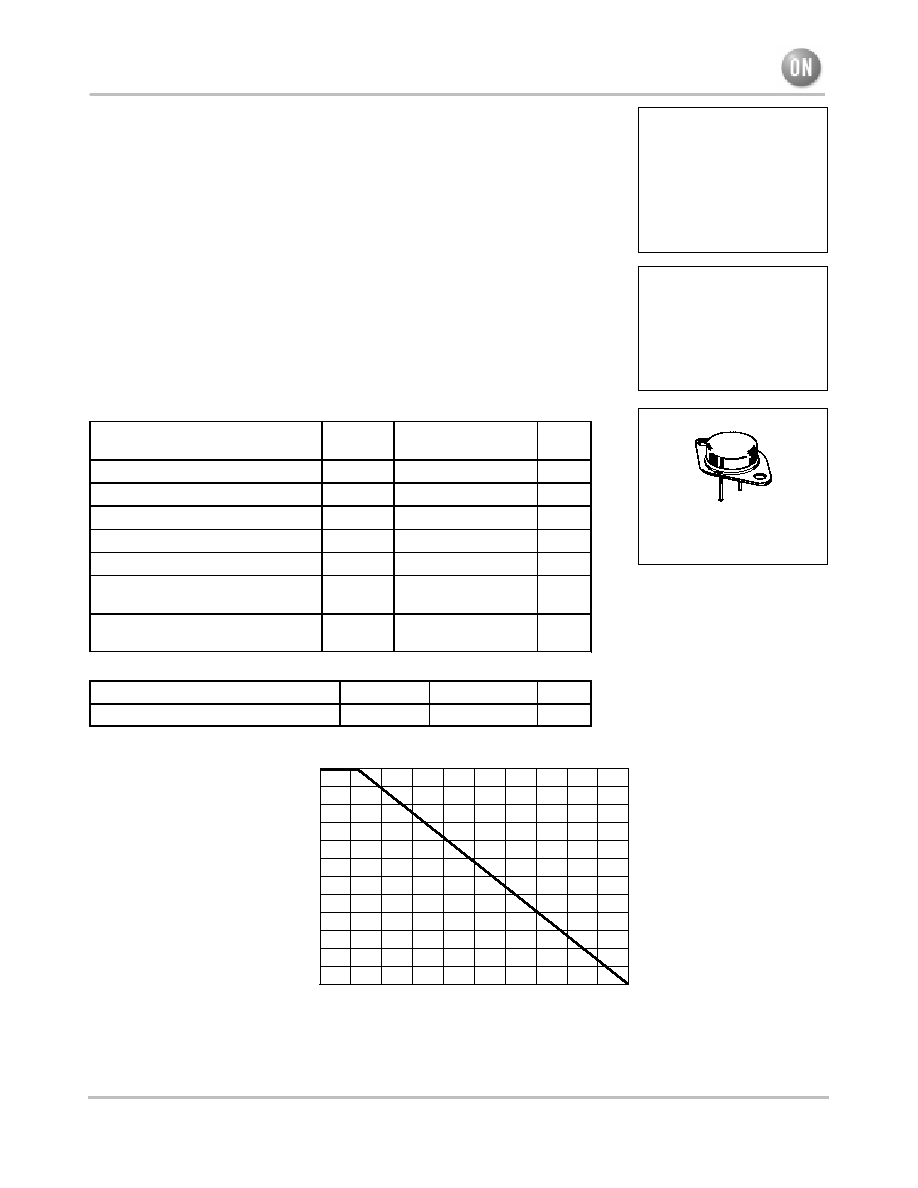
300
0
0
20
40
60
80
100
120 140 160 180 200
Figure 1. Power Derating
TEMPERATURE (
∞
C)
P D
, POWER DISSIP
A
TION (W
A
TTS)
250
150
100
50
200
Safe Area Curves are indicated by Figure 5. All limits are applicable and must be observed.
ON Semiconductort
©
Semiconductor Components Industries, LLC, 2001
May, 2001 ≠ Rev. 10
1
Publication Order Number:
2N5684/D
2N5684
2N5686
50 AMPERE
COMPLEMENTARY
SILICON
POWER TRANSISTORS
60≠80 VOLTS
300 WATTS
CASE 197A≠05
TO≠204AE
PNP
NPN

2N5684 2N5686
http://onsemi.com
2
ŒŒŒŒŒŒŒŒŒŒŒŒŒŒŒŒŒŒŒŒŒŒŒŒŒŒŒŒŒŒŒŒŒ
ŒŒŒŒŒŒŒŒŒŒŒŒŒŒŒŒŒŒŒŒŒŒŒŒŒŒŒŒŒŒŒŒŒ
*ELECTRICAL CHARACTERISTICS
(T
C
= 25
_
C unless otherwise noted)
ŒŒŒŒŒŒŒŒŒŒŒŒŒŒŒŒŒŒŒŒŒŒ
ŒŒŒŒŒŒŒŒŒŒŒŒŒŒŒŒŒŒŒŒŒŒ
Characteristic
ŒŒŒŒŒ
ŒŒŒŒŒ
Symbol
ŒŒŒ
ŒŒŒ
Min
ŒŒŒŒ
ŒŒŒŒ
Max
ŒŒŒ
ŒŒŒ
Unit
ŒŒŒŒŒŒŒŒŒŒŒŒŒŒŒŒŒŒŒŒŒŒŒŒŒŒŒŒŒŒŒŒŒ
ŒŒŒŒŒŒŒŒŒŒŒŒŒŒŒŒŒŒŒŒŒŒŒŒŒŒŒŒŒŒŒŒŒ
OFF CHARACTERISTICS
ŒŒŒŒŒŒŒŒŒŒŒŒŒŒŒŒŒŒŒŒŒŒ
Œ
ŒŒŒŒŒŒŒŒŒŒŒŒŒŒŒŒŒŒŒŒ
Œ
ŒŒŒŒŒŒŒŒŒŒŒŒŒŒŒŒŒŒŒŒŒŒ
Collector≠Emitter Sustaining Voltage (Note 2)
(I
C
= 0.2 Adc, I
B
= 0)
ŒŒŒŒŒ
Œ
ŒŒŒ
Œ
ŒŒŒŒŒ
V
CEO(sus)
ŒŒŒ
Œ
Œ
Œ
ŒŒŒ
80
ŒŒŒŒ
Œ
ŒŒ
Œ
ŒŒŒŒ
≠
ŒŒŒ
Œ
Œ
Œ
ŒŒŒ
Vdc
ŒŒŒŒŒŒŒŒŒŒŒŒŒŒŒŒŒŒŒŒŒŒ
ŒŒŒŒŒŒŒŒŒŒŒŒŒŒŒŒŒŒŒŒŒŒ
Collector Cutoff Current
(V
CE
= 40 Vdc, I
B
= 0)
ŒŒŒŒŒ
ŒŒŒŒŒ
I
CEO
ŒŒŒ
ŒŒŒ
≠
ŒŒŒŒ
ŒŒŒŒ
1.0
ŒŒŒ
ŒŒŒ
mAdc
ŒŒŒŒŒŒŒŒŒŒŒŒŒŒŒŒŒŒŒŒŒŒ
Œ
ŒŒŒŒŒŒŒŒŒŒŒŒŒŒŒŒŒŒŒŒ
Œ
ŒŒŒŒŒŒŒŒŒŒŒŒŒŒŒŒŒŒŒŒŒŒ
Collector Cutoff Current
(V
CE
= 80 Vdc, V
EB(off)
= 1.5 Vdc)
(V
CE
= 80 Vdc, V
EB(off)
= 1.5 Vdc, T
C
= 150
_
C)
ŒŒŒŒŒ
Œ
ŒŒŒ
Œ
ŒŒŒŒŒ
I
CEX
ŒŒŒ
Œ
Œ
Œ
ŒŒŒ
≠
≠
ŒŒŒŒ
Œ
ŒŒ
Œ
ŒŒŒŒ
2.0
10
ŒŒŒ
Œ
Œ
Œ
ŒŒŒ
mAdc
ŒŒŒŒŒŒŒŒŒŒŒŒŒŒŒŒŒŒŒŒŒŒ
Œ
ŒŒŒŒŒŒŒŒŒŒŒŒŒŒŒŒŒŒŒŒ
Œ
ŒŒŒŒŒŒŒŒŒŒŒŒŒŒŒŒŒŒŒŒŒŒ
Collector Cutoff Current
(V
CB
= 80 Vdc, I
E
= 0)
ŒŒŒŒŒ
Œ
ŒŒŒ
Œ
ŒŒŒŒŒ
I
CBO
ŒŒŒ
Œ
Œ
Œ
ŒŒŒ
≠
ŒŒŒŒ
Œ
ŒŒ
Œ
ŒŒŒŒ
2.0
ŒŒŒ
Œ
Œ
Œ
ŒŒŒ
mAdc
ŒŒŒŒŒŒŒŒŒŒŒŒŒŒŒŒŒŒŒŒŒŒ
ŒŒŒŒŒŒŒŒŒŒŒŒŒŒŒŒŒŒŒŒŒŒ
Emitter Cutoff Current (V
BE
= 5.0 Vdc, I
C
= 0)
ŒŒŒŒŒ
ŒŒŒŒŒ
I
EBO
ŒŒŒ
ŒŒŒ
≠
ŒŒŒŒ
ŒŒŒŒ
5.0
ŒŒŒ
ŒŒŒ
mAdc
ŒŒŒŒŒŒŒŒŒŒŒŒŒŒŒŒŒŒŒŒŒŒŒŒŒŒŒŒŒŒŒŒŒ
ŒŒŒŒŒŒŒŒŒŒŒŒŒŒŒŒŒŒŒŒŒŒŒŒŒŒŒŒŒŒŒŒŒ
ON CHARACTERISTICS
ŒŒŒŒŒŒŒŒŒŒŒŒŒŒŒŒŒŒŒŒŒŒ
Œ
ŒŒŒŒŒŒŒŒŒŒŒŒŒŒŒŒŒŒŒŒ
Œ
ŒŒŒŒŒŒŒŒŒŒŒŒŒŒŒŒŒŒŒŒŒŒ
DC Current Gain (Note 2)
(I
C
= 25 Adc, V
CE
= 2.0 Vdc)
(I
C
= 50 Adc, V
CE
= 5.0 Vdc)
ŒŒŒŒŒ
Œ
ŒŒŒ
Œ
ŒŒŒŒŒ
h
FE
ŒŒŒ
Œ
Œ
Œ
ŒŒŒ
15
5.0
ŒŒŒŒ
Œ
ŒŒ
Œ
ŒŒŒŒ
60
≠
ŒŒŒ
Œ
Œ
Œ
ŒŒŒ
≠
ŒŒŒŒŒŒŒŒŒŒŒŒŒŒŒŒŒŒŒŒŒŒ
Œ
ŒŒŒŒŒŒŒŒŒŒŒŒŒŒŒŒŒŒŒŒ
Œ
ŒŒŒŒŒŒŒŒŒŒŒŒŒŒŒŒŒŒŒŒŒŒ
Collector≠Emitter Saturation Voltage (Note 2)
(I
C
= 25 Adc, I
B
= 2.5 Adc)
(I
C
= 50 Adc, I
B
= 10 Adc)
ŒŒŒŒŒ
Œ
ŒŒŒ
Œ
ŒŒŒŒŒ
V
CE(sat)
ŒŒŒ
Œ
Œ
Œ
ŒŒŒ
≠
≠
ŒŒŒŒ
Œ
ŒŒ
Œ
ŒŒŒŒ
1.0
5.0
ŒŒŒ
Œ
Œ
Œ
ŒŒŒ
Vdc
ŒŒŒŒŒŒŒŒŒŒŒŒŒŒŒŒŒŒŒŒŒŒ
ŒŒŒŒŒŒŒŒŒŒŒŒŒŒŒŒŒŒŒŒŒŒ
Base≠Emitter Saturation Voltage (Note 1) (I
C
= 25 Adc, I
B
= 2.5 Adc)
ŒŒŒŒŒ
ŒŒŒŒŒ
V
BE(sat)
ŒŒŒ
ŒŒŒ
≠
ŒŒŒŒ
ŒŒŒŒ
2.0
ŒŒŒ
ŒŒŒ
Vdc
ŒŒŒŒŒŒŒŒŒŒŒŒŒŒŒŒŒŒŒŒŒŒ
ŒŒŒŒŒŒŒŒŒŒŒŒŒŒŒŒŒŒŒŒŒŒ
Base≠Emitter On Voltage (Note 1) (I
C
= 25 Adc, V
CE
= 2.0 Vdc)
ŒŒŒŒŒ
ŒŒŒŒŒ
V
BE(on)
ŒŒŒ
ŒŒŒ
≠
ŒŒŒŒ
ŒŒŒŒ
2.0
ŒŒŒ
ŒŒŒ
Vdc
ŒŒŒŒŒŒŒŒŒŒŒŒŒŒŒŒŒŒŒŒŒŒŒŒŒŒŒŒŒŒŒŒŒ
ŒŒŒŒŒŒŒŒŒŒŒŒŒŒŒŒŒŒŒŒŒŒŒŒŒŒŒŒŒŒŒŒŒ
DYNAMIC CHARACTERISTICS
ŒŒŒŒŒŒŒŒŒŒŒŒŒŒŒŒŒŒŒŒŒŒ
ŒŒŒŒŒŒŒŒŒŒŒŒŒŒŒŒŒŒŒŒŒŒ
Current≠Gain ≠ Bandwidth Product (I
C
= 5.0 Adc, V
CE
= 10 Vdc, f = 1.0 MHz)
ŒŒŒŒŒ
ŒŒŒŒŒ
f
T
ŒŒŒ
ŒŒŒ
2.0
ŒŒŒŒ
ŒŒŒŒ
≠
ŒŒŒ
ŒŒŒ
MHz
ŒŒŒŒŒŒŒŒŒŒŒŒŒŒŒŒŒŒŒŒŒŒ
ŒŒŒŒŒŒŒŒŒŒŒŒŒŒŒŒŒŒŒŒŒŒ
Output Capacitance
2N5684
(V
CB
= 10 Vdc, I
E
= 0, f = 0.1 MHz)
2N5686
ŒŒŒŒŒ
ŒŒŒŒŒ
C
ob
ŒŒŒ
ŒŒŒ
≠
≠
ŒŒŒŒ
ŒŒŒŒ
2000
1200
ŒŒŒ
ŒŒŒ
pF
ŒŒŒŒŒŒŒŒŒŒŒŒŒŒŒŒŒŒŒŒŒŒ
ŒŒŒŒŒŒŒŒŒŒŒŒŒŒŒŒŒŒŒŒŒŒ
Small≠Signal Current Gain (I
C
= 10 Adc, V
CE
= 5.0 Vdc, f = 1.0 kHz)
ŒŒŒŒŒ
ŒŒŒŒŒ
h
fe
ŒŒŒ
ŒŒŒ
15
ŒŒŒŒ
ŒŒŒŒ
≠
ŒŒŒ
ŒŒŒ
*Indicates JEDEC Registered Data.
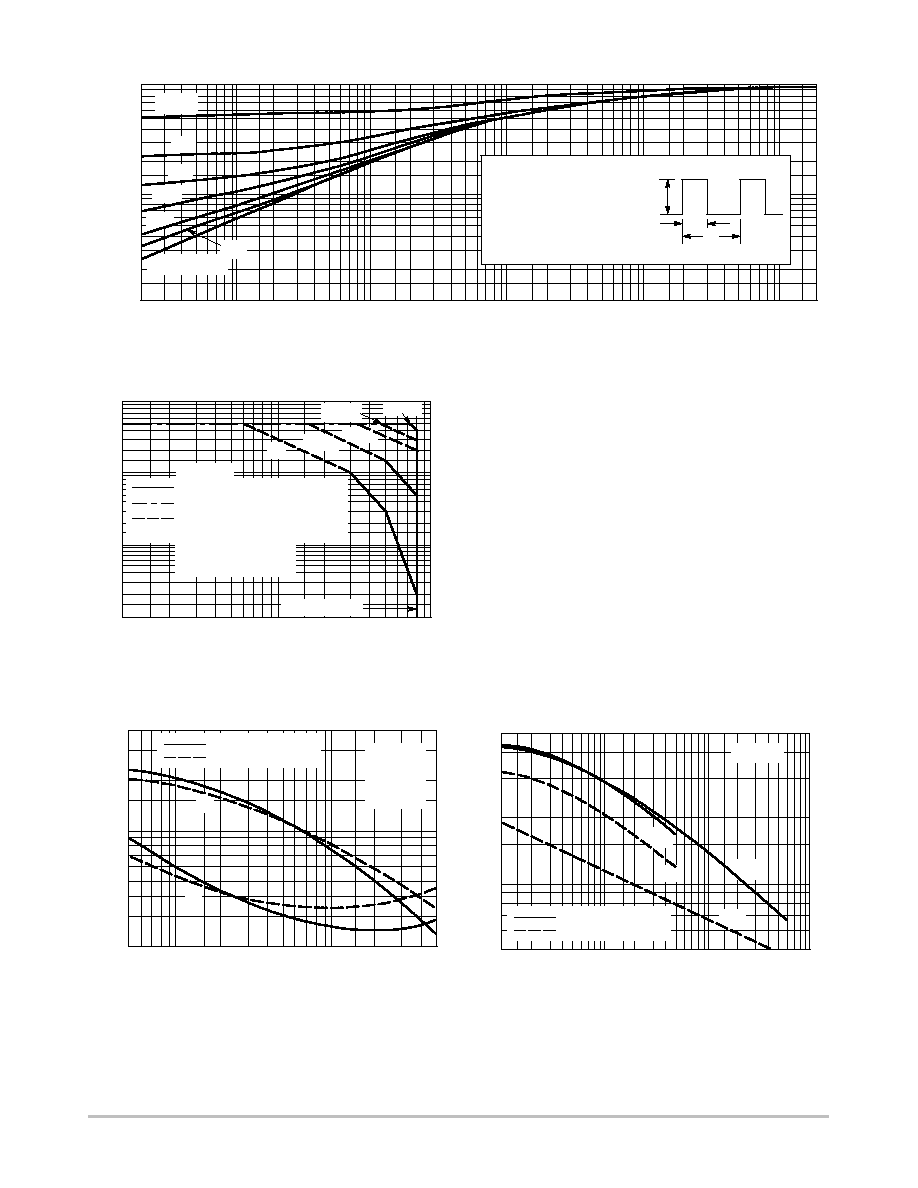
Note 2: Pulse Test: Pulse Width
v
300
µ
s, Duty Cycle
v
2.0%.
Figure 2. Switching Time Test Circuit
1.0
0.5
Figure 3. Turn≠On Time
I
C
, COLLECTOR CURRENT (AMP)
t, TIME
(s)
µ
0.7
0.5
0.2
0.07
0.05
0.02
0.01
0.7 1.0
2.0
3.0
5.0 7.0 10
50
T
J
= 25
∞
C
I
C
/I
B
= 10
V
CC
= 30 V
0.03
0.3
30
0.1
20
2N5684 (PNP)
2N5686 (NPN)
t
r
t
d
+2.0 V
0
t
r
20 ns
-12 V
10 to 100
µ
s
DUTY CYCLE
2.0%
R
B
R
L
V
CC
-30 V
TO SCOPE
t
r
20 ns
V
CC
-30 V
TO SCOPE
t
r
20 ns
R
L
R
B
+10 V
0
-12 V
10 to 100
µ
s
DUTY CYCLE
2.0%
t
r
20 ns
V
BB
+4.0 V
FOR CURVES OF FIGURES 3 & 6, R
B
& R
L
ARE VARIED.
INPUT LEVELS ARE APPROXIMATELY AS SHOWN.
FOR NPN CIRCUITS, REVERSE ALL POLARITIES.
2N5684 2N5686
http://onsemi.com
3
Figure 4. Thermal Response
t, TIME (ms)
1.0
0.01
0.02
0.7
0.5
0.3
0.2
0.1
0.07
0.05
0.03
0.02
r(t)
, EFFECTIVE
TRANSIENT
THERMAL
RESIST
ANCE (NORMALIZED)
0.05
0.1
0.2
0.5
1.0
2.0
5.0
10
20
50
100
200
2000
500
JC
(t) = r(t)
JC
JC
= 0.584
∞
C/W MAX
D CURVES APPLY FOR POWER
PULSE TRAIN SHOWN
READ TIME AT t
1
T
J(pk)
- T
C
= P
(pk)
JC
(t)
P
(pk)
t
1
t
2
DUTY CYCLE, D = t
1
/t
2
D = 0.5
0.05
0.02
0.01
SINGLE PULSE
0.1
1000
0.2
100
1.0
Figure 5. Active≠Region Safe Operating Area
V
CE
, COLLECTOR-EMITTER VOLTAGE (VOLTS)
50
20
10
5.0
0.1
2.0 3.0
7.0 10
20 30
50
100
SECOND BREAKDOWN LIMITED
BONDING WIRE LIMITED
THERMALLY LIMITED @ T
C
= 25
∞
C
(SINGLE PULSE)
70
2.0
I C
, COLLECT
OR CURRENT
(AMP)
T
J
= 200
∞
C
CURVES APPLY BELOW
RATED V
CEO
dc
1.0 ms
500
µ
s
1.0
0.5
0.2
5.0
100
µ
s
5.0 ms
2N5684, 2N5686
There are two limitations on the power handling ability of
a transistor: average junction temperature and second
breakdown. Safe operating area curves indicate I
C
≠ V
CE
limits of the transistor that must be observed for reliable
operation; i.e., the transistor must not be subjected to greater
dissipation than the curves indicate.
The data of Figure 5 is based on T
J(pk)
= 200
_C; T
C
is
variable depending on conditions. Second breakdown pulse
limits are valid for duty cycles to 10% provided T
J(pk)
v 200_C. T
J(pk)
may be calculated from the data in
Figure 4. At high case temperatures, thermal limitations will
reduce the power that can be handled to values less than the
limitations imposed by second breakdown.
4.0
0.5
Figure 6. Turn≠Off Time
I
C
, COLLECTOR CURRENT (AMP)
2.0
1.0
0.6
0.4
0.2
0.7 1.0
2.0 3.0
7.0
20
50
T
J
= 25
∞
C
I
B1
= I
B2
I
C
/I
B
= 10
V
CE
= 30 V
0.3
t, TIME
(s)
µ
t
s
5.0
5000
0.1
Figure 7. Capacitance
V
R
, REVERSE VOLTAGE (VOLTS)
500
2.0
5.0
10
20
100
50
0.2
0.5
1.0
C, CAP
ACIT
ANCE (pF)
3000
1000
700
T
J
= 25
∞
C
0.8
3.0
30
2000
10
2N5684 (PNP)
2N5686 (NPN)
t
f
C
ib
2N5684 (PNP)
2N5686 (NPN)
C
ob
C
ob
C
ib

2N5684 2N5686
http://onsemi.com
4
V CE
, COLLECT
OR-EMITTER VOL
T
AGE (VOL
TS)
V CE
, COLLECT
OR-EMITTER VOL
T
AGE (VOL
TS)
500
0.5
Figure 8. DC Current Gain
I
C
, COLLECTOR CURRENT (AMP)
5.0
0.7 1.0
2.0
5.0 7.0 10
20
50
70
30
20
10
100
50
h FE
, DC CURRENT
GAIN
T
J
= +150
∞
C
+25
∞
C
-55
∞
C
7.0
200
300
V
CE
= 2.0 V
V
CE
= 10 V
3.0
30
PNP
2N5684
I
C
, COLLECTOR CURRENT (AMP)
h FE
, DC CURRENT
GAIN
T
J
= +150
∞
C
+25
∞
C
-55
∞
C
V
CE
= 2.0 V
V
CE
= 10 V
NPN
2N5686
Figure 9. Collector Saturation Region
2.0
0.1
I
B
, BASE CURRENT (AMP)
0
0.2
1.0
2.0
5.0
10
0.8
0.4
I
C
= 10 A
T
J
= 25
∞
C
25 A
1.2
1.6
0.5
3.0
40 A
0.1
I
B
, BASE CURRENT (AMP)
0.2
1.0
2.0
5.0
10
I
C
= 10 A
T
J
= 25
∞
C
25 A
0.5
3.0
40 A
0.3
2.5
0.5
I
C
, COLLECTOR CURRENT (AMP)
0.7 1.0
2.0 3.0
5.0
10
20
50
2.0
1.5
1.0
0.5
0
T
J
= 25
∞
C
V
BE(sat)
@ I
C
/I
B
= 10
V
CE(sat)
@ I
C
/I
B
= 10
V
,
VOL
T
AGE (VOL
TS)
Figure 10. "On" Voltages
30
V
BE
@ V
CE
= 2.0 V
7.0
2.0
0.5
I
C
, COLLECTOR CURRENT (AMP)
0.7 1.0
2.0
3.0
5.0
10
20
50
1.6
1.2
0.8
0.4
0
T
J
= 25
∞
C
V
BE(sat)
@ I
C
/I
B
= 10
V
CE(sat)
@ I
C
/I
B
= 10
V
,
VOL
T
AGE (VOL
TS)
30
V
BE
@ V
CE
= 2.0 V
500
0.5
5.0
0.7 1.0
2.0
5.0 7.0 10
20
50
70
30
20
10
100
50
7.0
200
300
3.0
30
2.0
0
0.8
0.4
1.2
1.6

2N5684 2N5686
http://onsemi.com
5
PACKAGE DIMENSIONS
CASE 197A≠05
TO≠204AE
ISSUE J
NOTES:
1. DIMENSIONING AND TOLERANCING PER ANSI
Y14.5M, 1982.
2. CONTROLLING DIMENSION: INCH.
STYLE 1:
PIN 1. BASE
2. EMITTER
CASE: COLLECTOR
DIM
MIN
MAX
MIN
MAX
MILLIMETERS
INCHES
A
1.530 REF
38.86 REF
B
0.990
1.050
25.15
26.67
C
0.250
0.335
6.35
8.51
D
0.057
0.063
1.45
1.60
E
0.060
0.070
1.53
1.77
G
0.430 BSC
10.92 BSC
H
0.215 BSC
5.46 BSC
K
0.440
0.480
11.18
12.19
L
0.665 BSC
16.89 BSC
N
0.760
0.830
19.31
21.08
Q
0.151
0.165
3.84
4.19
U
1.187 BSC
30.15 BSC
V
0.131
0.188
3.33
4.77
A
N
E
C
K
≠T≠
SEATING
PLANE
2 PL
D
M
Q
M
0.30 (0.012)
Y
M
T
M
Y
M
0.25 (0.010)
T
≠Q≠
≠Y≠
2
1
L
G
B
V
H
U