
©
Semiconductor Components Industries, LLC, 2003
June, 2003 - Rev. 1
1
Publication Order Number:
AND8098/D
AND8098/D
Low-Cost 100 mA
High-Voltage Buck and
Buck-Boost Using NCP1052
Prepared by: Kahou Wong
ON Semiconductor
INTRODUCTION
This application note presents low-cost high-voltage
100 mA non-isolated power supply using NCP1052 by
buck and buck-boost topology. The NCP1052 is one of the
latest low-cost switching controllers with integrated 700 V/
300 mA power switch from ON Semiconductor. It is
primarily designed for isolated 10 W-range flyback
converter. If isolation is not needed, the IC can also be used
as stepping-down buck and buck-boost converter for
further cost saving by removing optocoupler and replacing
the transformer by an inductor. The output current capability
is 100 mA. The possible operating range is from input range
between 20 Vdc and 700 Vdc to output range of 5.0 V or
above with 100 mA. Typical efficiency around 65% is
obtained in the 12 V buck demo board.
Advantages of the proposed circuits include:
∑
Comparing to flyback, buck and buck-boost eliminates
optocoupler and replaces transformer by an inductor for
cost saving.
∑
Buck and buck-boost offers smaller voltage stress in
switches comparing to flyback. It minimizes the
switching loss and increases efficiency.
∑
NCP105x can power up itself from the high input
voltage with wide range between 20 Vdc and 700 Vdc.
It needs no extra supply circuit.
∑
NCP105x operates at 44, 100, or 136 kHz and
accommodates low-cost components such as aluminum
electrolytic capacitors and powered-iron core magnetic.
∑
NCP105x offers frequency jittering for reduced
electromagnetic inference (EMI).
∑
NCP105x offers thermal and short circuit fault
protection.
∑
Simple design as no control-loop compensation is
concerned.
The proposed buck and buck-boost converters are very
similar to each other. Their major difference is that buck
provides a positive output voltage but buck-boost provides
a negative output voltage referring to the input ground.
PRINCIPLE OF OPERATION
Figure 1 shows the proposed buck and buck-boost
converters. The rectifier circuit, which consists of capacitor
C
3
and diode D
3
, is in the front end for AC or DC input
voltage. Then, the NCP1052 is self-powered up from the
rectified input voltage directly with a V
CC
capacitor C
2
.
When the switch inside the IC is opened, there is a voltage
across Drain (D) and Source (S) pins of the IC. If this voltage
is greater than 20 V, an internal current source I
start
= 6.3 mA
(typ.) inside the IC charges up C
2
and a voltage in C
2
is built
up for the operation of the IC. Comparing to the switching
frequency, the V
CC
voltage level is in a lower-frequency
7.5-8.5 V hysteresis loop. This V
CC
hysteresis loop is for
frequency jittering features to minimize EMI and
short-circuit fault timing function.
Input
Output
D
3
C
3
D
L
C
1
C
Z
1
C
2
V
CC
FB
D
S
D
2
Z
2
D
1
R
1
(a) Buck
Input
Output
D
3
C
3
D
L
C
1
C
Z
1
C
2
V
CC
FB
D
S
D
2
Z
2
D
1
R
1
(b) Buck-boost
Figure 1. Proposed Circuit Using NCP1052
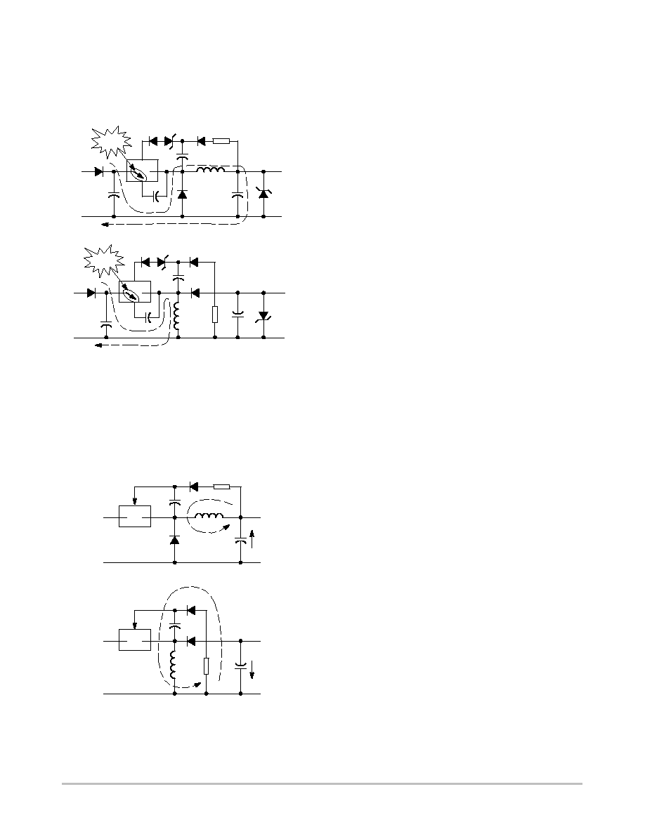
In Figure 2a it is noted that in the buck topology the input
voltage powers up the IC through the path across the
inductor L and capacitor C. This charging path passes
APPLICATION NOTE
http://onsemi.com
AND8098/D
http://onsemi.com
2
through the output and a low-frequency ripple will be found
in the output voltage. Hence, the value of C
2
is needed to be
small enough to increase this charging frequency f
VCC
in
order to reduce output voltage ripple because some
efficiency is lost due to this low-frequency ripple.
Input
Output
D
3
C
3
D
L
C
1
C
Z
1
C
2
V
CC
FB
D
S
D
2
Z
2
D
1
R
1
(a) Buck
Input
Output
D
3
C
3
D
L
C
1
C
Z
1
C
2
V
CC
FB
D
S
D
2
Z
2
D
1
R
1
(b) Buck-boost
I
start
I
start
Figure 2. Charging Current of C
2
In Figure 2b it is noted that in the buck-boost topology the
charging current path is blocked by diode D and hence the
charging of C
2
does not affect the output voltage directly.
However, it still affects the output voltage indirectly and
slightly by adding some low-frequency noise on the
inductor. Hence, small value of C
2
is also wanted.
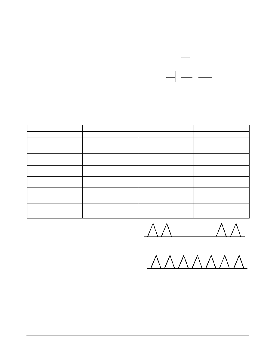
C
1
V
out
R
1
(a) Buck
D
1
C
1
V
out
R
1
(b) Buck-boost
D
1
Figure 3. Output Voltage Couples to C
1
with a
Charging Current
The function of diode D
1
, capacitor C
1
and resistor R
1
are
to transfer the magnitude of output voltage to a voltage
across C
1
so that the IC can regulate the output voltage. In
Figure 3, when the main switch inside the IC is opened and
the diode D is closed. In buck, the potential of the IC
reference ground (pin S) becomes almost 0 V in this
moment. In buck-boost, the potential of the IC reference
ground (pin S) becomes -V
out
in this moment. The voltage
in C
1
will be charged to the output voltage. On the other
hand, when main switch is closed and the diode D is opened,
diode D
1
is reverse biased by a voltage with magnitude V
in
and V
in
+V
out
respectively. Hence, D
1
does not affect the
normal operation of the buck and buck-boost converter.
It is noted that the instantaneous voltage in C
1
can be
possibly greater than the output voltage especially when
output current or output ripple is too large. It directly affects
the load regulation of the circuit since the IC regulates the
output voltage based on the voltage in C
1
. In order to solve
it, larger values of L and R
1
can help to slow down the
charging speed of C
1
. It reduces the maximum instantaneous
voltage in C
1
so that output voltage at high output current
can be pulled up and a good regulation is made.
Larger value of L can help the load regulation but it
usually unwanted because it is bulky. Hence, resistor R
1
is
recommended. Larger value of R
1
makes higher output
voltage. Hence, it is called as a "pull-up resistor" and it can
help to pull up the output voltage slightly.
The voltage in C
1
representing the output voltage is
feedback to the feedback (FB) pin of the NCP1052 through
a diode D
2
and zener diode Z
2
. When output voltage is too
high, there will be a greater-than-50
mA current inserting
into the feedback pin of the NCP1052. The NCP1052 will
stop switching when it happens. When output voltage is not
high enough, the current inserting into the feedback is
smaller than 50
mA. The NCP1052 enables switching and
power is delivered to the output until the output voltage is
too high again.
The purpose of the diode D
2
is to ensure the current is
inserting into the feedback pin because the switching of
NCP1052 can also be stopped when there is a
greater-than-50
mA current sinking from the FB pin. The
purpose of the zener diode Z
2
is to set the output voltage
threshold. The FB pin of NCP1052 with a condition of
50
mA sourcing current is about 4.3 V. The volt-drop of the
diode D
2
is loosely about 0.7 V at 50
mA. Hence, the output
voltage can be loosely set as follows:
Vout
+
zener
)
4.3 V
)
0.7 V
(eq. 1)
+
zener
)
5 V
According to (1), the possible minimum output voltage of
the circuit is 5.0 V when there is no zener diode Z
2
.
If there is no load, the IC will automatically minimize its
duty cycle to the minimum value but the output voltage is
still possible to be very high because there is no passive
component in the circuit try to absorb the energy. As a result,
AND8098/D
http://onsemi.com
3
output voltage will rise up dramatically and burn the output
capacitor eventually. Hence, a zener diode Z
1
or minimum
"dummy" load resistor is needed to consume the minimum
amount of energy as shown in Figure 1. It is also noted that
when R
1
pulls up the output voltage at a given output current
condition, the output voltages at lower output current
conditions are also pulled up. Hence, the clamping zener
diode Z
1
is needed to be with the breakdown voltage as same
as the output voltage but it will reduce some of the efficiency
at lower output current conditions.
DESIGN CONSIDERATION
Topology
Buck circuit is to step down a voltage. Buck-boost circuit
is to step up or down a voltage. The output voltage is
inverted. The maximum duty of NCP1052 is typically 77%.
Because of burst-mode control, the effective maximum
duty is lower and said to be 70% roughly. When a buck
converter is in continuous conduction mode (CCM), the
input voltage V
in
and output voltage V
out
are related by the
duty ratio D.
Vout
Vin
+
D
t
0.7
(eq. 2)
The relationship in buck-boost is
Vout
Vin
+
D
1
*
D
t
0.7
1
*
0.7
+
2.33
(eq. 3)
Another aspect on topology is the output current. The
maximum output current is always smaller than the
maximum switch current in non-isolated topologies.
However, in isolated topologies such as flyback the
maximum output current can be increased by a transformer.
Table 1. Summary of Topology Difference Using NCP1052
Buck
Buck-boost
Flyback
Output voltage
< 0.7 V
in
Negative & < 2.33 Vin
Depending on transformer ratio
Output current
< 300 mA
<< 300 mA, output current is
only a portion of the inductor
current
< 10 W. It depends on operating
condition and audible noise level
Input voltage
< 700 V
t
700
*
Vout V
t
700 V
<< 700 V. It depends on
transformer ratio
Operating mode in nominal
condition
Continuous
Continuous
Discontinuous
Standby ability on V
CC
charging
current
Bad. The current flows through
output even if there is no load
Good. The current passes
through inductor only
Good. The current passes
through primary winding only
Transformer / Auxiliary winding
It is only for standby
improvement or additional
output
It is only for standby
improvement or additional
output
It is a must for the main output.
Additional auxiliary winding can
improve standby performance
Isolation
No
No
Yes. Opto coupler can be
eliminated if isolation is not
needed
Burst-mode Operation
The NCP1052 is with a burst-mode control method. It
means the MOSFET can be completely off for one or more
switching cycles. The output voltage is regulated by the
overall duration of dead time or non-dead time over a
number of switching cycles. This feature offers advantages
on saving energy in standby condition since it can reduce the
effective duty cycle dramatically. In flyback topology, the
circuit is mainly designed for discontinuous conduction
mode (DCM) in which the inductor current reaches zero in
every switching cycle. The DCM burst-mode waveform can
be represented in Figure 4. It is similar to the pulse-width
modulation (PWM) one.
Figure 4. DCM Inductor Currents in Burst Mode
and PWM Control
Burst mode
PWM

AND8098/D
http://onsemi.com
4
In non-isolated topologies such as buck or buck-boost,
the circuits are mainly designed for CCM. The CCM
burst-mode waveform is different to the PWM waveform in
Figure 5. Because of this characteristic, burst mode requires
a higher peak value of the inductor current in order to have
the same level of averaged inductor current (or output
current).
Figure 5. CCM Inductor Currents in Burst Mode
and traditional PWM Control
Burst mode
PWM
As shown in Figure 4 and 5 burst-mode control produces
low-frequency waveform comparing to the switching
frequency. Part of the power loss in this low frequency
becomes audible noise. Therefore, burst-mode control is
not suitable for high power applications such as more than
20 W.
V
CC
Capacitor
The V
CC
capacitor C
2
is the key component to make the
circuit operate in normal mode or fault mode. The device
recognizes a fault condition when there is no feedback
current in the FB pin during the time from V
CC
= 8.5 V to
7.5 V. The V
CC
capacitor directly affects this time duration.
In normal mode, the V
CC
follows a 8.5 V-7.5 V-8.5 V
hysteresis loop. When the circuit is in fault mode, the V
CC
follows a 8.5 V-7.5 V-4.5 V-8.5 V hysteresis loop. The
device keeps its MOSFET opened except for the time from
V
CC
= 8.5 V to 7.5 V and delivers a little amount of power
to the output in fault mode.
A common and extreme case to enter fault condition is the
startup. The MOSFET begins switching at the V
CC
is firstly
charged to 8.5 V and hence output voltage rises. The output
voltage needs some time to build up the output voltage from
0 V to a desired value. When the desired level is reached, a
feedback current flows into the device to stop its switching.
If the feedback current is determined before V
CC
reaches
7.5V, the circuit will remain in normal mode. Otherwise, the
circuit will enter the fault mode and cannot provide the
output voltage at its desired level. Therefore, the V
CC
capacitor is needed to be big enough to ensure sufficient time
for V
CC
going from 8.5 V to 7.5 V to sample feedback
current in startup.
Figure 6. Startup Scenarios of the Circuits with
Big Enough or Too Small V
CC
Capacitor
Output waveforms with big enough V
CC
capacitor
time
FB current
V
CC
V
out
Output waveforms with too small V
CC
capacitor
time
V
CC
V
out
Desired level of V
out
Practically, the NCP1052 consumes approximately 0.5
mA in normal operation. The concerned fault sampling time
for feedback signal is from 8.5 V to 7.5V. Hence,
C
+
I
dt
dV
+
0.5
10- 3
1
∑ sampling time
(eq. 4)
+
0.5
10- 3 ∑ sampling time
For example, if sampling time or startup transient is
designed to be 20 ms, 10
µ
F V
CC
capacitor is needed.
Inductor
The 300 mA current limit in the NCP1052 is measured
with a condition that the di/dt reaches 300 mA in 4
µ
s. When
the buck or buck-boost circuit is designed for universal ac
input voltage (85 to 265 Vac), the rectified input voltage will
be possibly as high as 375 Vdc. In order to keep the 4
µ
s
condition, the inductance value will be 5 mH by (5) and (6).
For buck,
di
dt
+
Vin
*
Vout
L
[
Vin
L
(eq. 5)
For buck-boost,
di
dt
+
Vin
L
(eq. 6)
The 5 mH is practically too high and hence not very
practical. Therefore, the inductor is basically selected by
market available inductor models which is with a normally
smaller inductance (but not too small). It must have enough
saturation current level (>300 mA). If inductance is too

AND8098/D
http://onsemi.com
5
small, the di/dt becomes too high and the NCP1052 will
have a very high current limit effectively because there is a
propagation delay (typically 135 ns) to turn off the switch.
The current flowing through the inductor L includes three
parts. First, there is a V
CC
charging current I
start
in Figure 2.
It happens when V
CC
needs charging. Its magnitude is 6.3
mA. It is noted that the V
CC
discharging current does not
flow through the inductor. Second, it is the main inductor
current to deliver the output current. It is noted that the peak
of burst-mode inductor current is higher than PWM one as
in Figure 5 for the same level of averaged inductor current
(or output current). Finally, there is a current flowing
through diode D
1
to charge up C
1
. It also flows through the
inductor as shown in Figure 3. Its magnitude is a
greater-than-50
µ
A current and practically it is about 1 mA.
Hence, the saturation current of the inductor L is needed to
be bigger than their sum.
Another consideration on the inductor is the low-pass
filtering capability for the V
CC
hysteresis low frequency
(and the 50/ 60 Hz rectified AC line voltage ripple). As
shown in Figure 2, there is a low-frequency charging current
with magnitude 6.3 mA flowing through the inductor and
causes low-frequency ripple in the output voltage. A higher
value of the inductance can help to reduce the output ripple.
It is noted that when the output power is higher, the startup
time becomes longer. It needs bigger V
CC
capacitor and
makes lower V
CC
charging frequency. As a result, a bigger
inductance is needed.
The last consideration is the effect of load regulation.
Large inductor can limit the inrush current flowing into
capacitor C
1
as shown in Figure 3. High inrush current is not
desirable because it can make the C
1
voltage higher than the
output voltage. It makes load regulation poor. If there is no
pull-up resistor R
1
, inductor value L is chosen to be as large
as possible, say 2 mH.
Output Capacitor
Because of the burst-mode characteristic and the
low-frequency V
CC
charging current, the output ripple is
larger than those in PWM. Hence, a relatively bigger output
capacitor is needed to keep output ripple small. However,
big output capacitor needs a long time to build up the output
voltage initially and hence the circuit may enter into fault
mode in the startup in Figure 6.
Buffering Capacitor
Buffering capacitor C
2
is to provide a greater-than-50
µ
A
to the feedback pin of NCP1052. It is relatively much
smaller than the output capacitor because the current
consumption in this capacitor is much smaller and the output
voltage cannot copy to this buffering capacitor if the
buffering capacitor voltage is higher than the output voltage.
Diodes
D and D
1
are recommended to be the same part for
compatibility in speed and voltage drop. It helps the voltage
in the capacitor C
1
to be similar to the output voltage. The
reverse blocking voltage of D and D
1
is needed to be large
enough to withstand the input voltage in buck and input
voltage plus output voltage in buck-boost respectively.
D
2
is not a critical component. Its function is to make sure
that feedback current is only in one direction. The accuracy
of its voltage drop used in (1) is not important since the 4.3V
reference voltage in the NCP1052 is loosely set.
Zener Diodes
Z
1
is to clamp the output voltage when there is light load
or no load. Hence, the accuracy of Z
1
helps the regulation
accuracy in the light load or no load condition. It is also the
main component to consume energy when the circuit is in no
load condition. The output voltage is clamped and hence the
output capacitor is protected.
Z
2
and R
1
are to set the output voltage at the nominal load
current. Hence, their accuracy affects the regulation
accuracy at the nominal load condition. The relationship
between zener voltage and output voltage is shown in (1).
Higher value of R
1
helps to pull up the output voltage higher
by reducing the charging rate of the buffering capacitor C
1
.
Standby Condition
The standby ability of the proposed buck converter is not
good. It is because there is a V
CC
charging current I
start
flows
through the output capacitor in Figure 2(a). This charging
current is a low-frequency pulsating signal. As a result, the
voltage in the output capacitor continuously rises up by the
charging current pulses. In order to prevent over voltage in
the output capacitor, the zener Z
1
absorbs the charging
current. It consumes main portion of energy in standby.

AND8098/D
http://onsemi.com
6
The proposed buck-boost is better in term of the standby
ability. It is because the V
CC
charging current in Figure 2(b)
only passes through the inductor. The charging current
pulses become an averaged energy stored in the inductor and
consume smaller amount of power comparing to the buck
case.
Figure 7. Auxiliary Winding to improve standby
Abillity
(a) Buck
(b) Buck-boost
The auxiliary winding to supply the V
CC
voltage in Figure
7 is a method to improve the standby ability. The auxiliary
winding keeps the V
CC
voltage above 7.5 V and disable the
V
CC
charging current and hence its standby loss. The
auxiliary winding is coupled from the inductor L with
polarity same as the regulated output voltage. The V
CC
voltage in the auxiliary winding is designed to be between
the normal V
CC
limits of 7.5 and 8.5 V typically. The
frequency jittering feature loses when the V
CC
voltage is
fixed. When output is shorted, there will be no voltage
coming from the auxiliary winding and the circuit will enter
fault mode with the 4.5 V-8.5 V-7.5 V-4.5 V hysteresis
loop.
Another method to supply the V
CC
voltage is coupling
capacitor technique in Figure 8. The output voltage is
coupled to the inserted capacitor when the diodes are closed.
The voltage drop of the diodes compensate each other.
Hence, the diode voltage drop effect can be neglected. The
NCP1052 needs a nominal V
CC
voltage of 8V. The inserted
resistor consumes some voltage from the output voltage V
out
to make a 8V to the V
CC
pin. Based on the 0.5mA typical
current consumption of V
CC
pin. The inserted resistance
value is (V
out
- 8) / 0.5 k
W.
Figure 8. Coupling Capacitor Technique to
Improve Standby Abillity
(a) Buck
(b) Buck-boost
Temperature Rise
The NCP1052 is a very compact package with the control
circuit and high-voltage power switch. Its typical on
resistance is 22
. Temperature rise exists. It is
recommended to design the PCB board with a large copper
area next to the device as a heatsink. This heatsink decreases

AND8098/D
http://onsemi.com
7
the temperature rise and reduces the on resistance. Finally,
the efficiency of the circuit is benefited.
EXAMPLES
12 V / 100 mA NCP1052 Buck Demo Board
Figure 9. Layout of the Demo Board
As shown in Figure 9, a 2 inch by 1.5 inch small
surface-mount demo board of 12 V / 100 mA buck is
presented. The design is made on a single-sided board. The
bill of material is shown in Table 2. The component symbols
are those in Figure 1. In order to have sufficient startup
ability, the V
CC
capacitor is 6.8
µ
F which gives a 3.4 ms fault
sampling time. Because of this feature, the circuit enters
fault mode when output current exceeds 200mA after startup
as shown in Figure 10(b). The efficiency of the circuit is
typically 65% at 100 mA.
Table 2. Bill of Material of Buck Demo Board
Part No
Description
Manufacturer
IC
NCP1052ST136
Switching Regulator
ON Semiconductor
D, D
1
MURS160T3
1A 600V ultrafast
ON Semiconductor
D
2
MMSD914T1
General diode
ON Semiconductor
D
3
MRA4005T1
1A 600V standard recovery
ON Semiconductor
Z
1
MMSZ12T1
12V 5% zener
ON Semiconductor
Z
2
MMSZ6V8T1
6.8V 5% zener
ON Semiconductor
R
1
CRCW08052001FRT1
2 k
Vishay
C
594D227X9016R2T
220
µ
F, 16 V, tantalum
Vishay
C
1
VJ1206Y224KXXAT
0.22
µ
F, 25 V, ceramic
Vishay
C
2
595D685X9016A2T
6.8
µ
F, 16V, tantalum
Vishay
C
3
400WA10M12.5X16
400V 10
µ
F
Rubycon
L
UP2B-681
680
µ
H
Cooper

AND8098/D
http://onsemi.com
8
Figure 10. 12V / 100mA Buck Performance
OUTPUT CURRENT (mA)
150
10
50
4
350
0
OUTPUT VOL
T
AGE (V)
0
14
2
6
8
250
200
100
12
300
V
IN
= 100 Vdc
V
IN
= 300 Vdc
V
IN
= 200 Vdc
OUTPUT CURRENT (mA)
150
50
50
20
300
0
EFFICIENCY (%)
0
80
10
30
40
250
200
100
60
V
IN
= 100 Vdc
V
IN
= 300 Vdc
V
IN
= 200 Vdc
70
(a) Load Regulation
(b) Efficiency
Dual Output Buck-boost with Increased Output
Current Capability
Replacing NCP1052 by NCP1055, which is with a current
limit of 680 mA, the output current capability is increased.
Larger value of inductor L is selected for high current. On
the other hand, the current consumption of NCP1055 is
higher than NCP1052 and the startup transient time is longer
in a higher power application. Hence, the V
CC
capacitor is
increased. When the V
CC
capacitor increased, its charging
frequency is decreased. Output capacitor is also needed to be
increased to reduce this lower-frequency charging current/
ripple.
In addition, by adding one more auxiliary winding to the
inductor a secondary output is made. A typical example is
shown in Figure 11. In higher output current application, the
load regulation is the major problem. The 5.1k
resistor
plays an important role for the load regulation. The primary
output voltage is higher than the secondary because it can
increase the output current ability by stepping up the current
in the transformer. The line regulation is shown in Figure 12
when the output currents are constant.
Figure 11. Dual Output Buck-boost
Universal
AC Input
GND
1N4005
10
µ
F
1N4005 1N4746
MUR160
5.1k
MUR160
MUR160
22
µ
F
1
µ
F
150
µ
F
220
µ
F
-24V / 200mA
-5V / 150mA
1.2mH / 92.3
µ
H
NCP1055P100

AND8098/D
http://onsemi.com
9
Figure 12. Line Regulation of the Dual Output
Buck-boost
INPUT VOLTAGE (Vac)
150
-10
50
300
OUTPUT VOL
T
AGE (V)
-25
0
-20
-15
250
200
100
-5
Output 1 with 200 mA
Output 2 with 150 mA
CONCLUSION
100 mA high-voltage low-cost buck and buck-boost
circuits using NCP1052 are presented. These circuits are
designed for cost-saving non-isolated application so that
optocoupler and transformer are saved. The possible input
voltage range is from 20 Vdc to 700 Vdc so that it is suitable
for general AC/DC and DC/DC applications with positive or
negative output voltages. It is noted that the standby ability
of the circuits is not good because of the V
CC
capacitor
charging current. However, it can be improved by adding an
auxiliary winding to the V
CC
. The design consideration of
each component in the circuits is explained. By replacing the
NCP1052 with NCP1055, the output current can be
increased. By adding an auxiliary winding, multi-output can
be obtained. A 12 V / 100 mA demo board is presented with
typical 65% efficiency.

AND8098/D
http://onsemi.com
10
ON Semiconductor and are registered trademarks of Semiconductor Components Industries, LLC (SCILLC). SCILLC reserves the right to make
changes without further notice to any products herein. SCILLC makes no warranty, representation or guarantee regarding the suitability of its products for any
particular purpose, nor does SCILLC assume any liability arising out of the application or use of any product or circuit, and specifically disclaims any and all
liability, including without limitation special, consequential or incidental damages. "Typical" parameters which may be provided in SCILLC data sheets and/or
specifications can and do vary in different applications and actual performance may vary over time. All operating parameters, including "Typicals" must be
validated for each customer application by customer's technical experts. SCILLC does not convey any license under its patent rights nor the rights of others.
SCILLC products are not designed, intended, or authorized for use as components in systems intended for surgical implant into the body, or other applications
intended to support or sustain life, or for any other application in which the failure of the SCILLC product could create a situation where personal injury or death
may occur. Should Buyer purchase or use SCILLC products for any such unintended or unauthorized application, Buyer shall indemnify and hold SCILLC
and its officers, employees, subsidiaries, affiliates, and distributors harmless against all claims, costs, damages, and expenses, and reasonable attorney fees
arising out of, directly or indirectly, any claim of personal injury or death associated with such unintended or unauthorized use, even if such claim alleges that
SCILLC was negligent regarding the design or manufacture of the part. SCILLC is an Equal Opportunity/Affirmative Action Employer.
PUBLICATION ORDERING INFORMATION
JAPAN: ON Semiconductor, Japan Customer Focus Center
2-9-1 Kamimeguro, Meguro-ku, Tokyo, Japan 153-0051
Phone: 81-3-5773-3850
ON Semiconductor Website: http://onsemi.com
For additional information, please contact your local
Sales Representative.
AND8098/D
Literature Fulfillment:
Literature Distribution Center for ON Semiconductor
P.O. Box 5163, Denver, Colorado 80217 USA
Phone: 303-675-2175 or 800-344-3860 Toll Free USA/Canada
Fax: 303-675-2176 or 800-344-3867 Toll Free USA/Canada
Email: ONlit@hibbertco.com
N. American Technical Support: 800-282-9855 Toll Free USA/Canada