 | –≠–ª–µ–∫—Ç—Ä–æ–Ω–Ω—ã–π –∫–æ–º–ø–æ–Ω–µ–Ω—Ç: 4066 | –°–∫–∞—á–∞—Ç—å:  PDF PDF  ZIP ZIP |

©
Semiconductor Components Industries, LLC, 2000
March, 2000 ≠ Rev. 3
1
Publication Order Number:
MC14066B/D
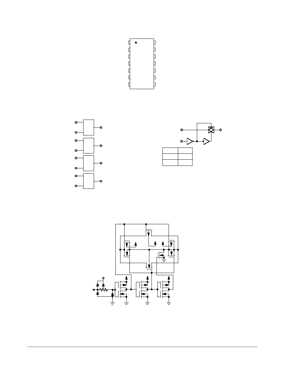
MC14066B
Quad Analog Switch/Quad
Multiplexer
The MC14066B consists of four independent switches capable of
controlling either digital or analog signals. This quad bilateral switch
is useful in signal gating, chopper, modulator, demodulator and
CMOS logic implementation.
The MC14066B is designed to be pin≠for≠pin compatible with the
MC14016B, but has much lower ON resistance. Input voltage swings
as large as the full supply voltage can be controlled via each
independent control input.
∑
Triple Diode Protection on All Control Inputs
∑
Supply Voltage Range = 3.0 Vdc to 18 Vdc
∑
Linearized Transfer Characteristics
∑
Low Noise -- 12 nV/
Cycle, f
1.0 kHz typical
∑
Pin≠for≠Pin Replacement for CD4016, CD4016, MC14016B
∑
For Lower R
ON
, Use The HC4066 High≠Speed CMOS Device
MAXIMUM RATINGS
(Voltages Referenced to V
SS
) (Note 2.)
Symbol
Parameter
Value
Unit
V
DD
DC Supply Voltage Range
≠ 0.5 to +18.0
V
V
in
, V
out
Input or Output Voltage Range
(DC or Transient)
≠ 0.5 to V
DD
+ 0.5
V
I
in
Input Current (DC or Transient)
per Control Pin
±
10
mA
I
SW
Switch Through Current
±
25
mA
P
D
Power Dissipation,
per Package (Note 3.)
500
mW
T
A
Ambient Temperature Range
≠ 55 to +125
∞
C
T
stg
Storage Temperature Range
≠ 65 to +150
∞
C
T
L
Lead Temperature
(8≠Second Soldering)
260
∞
C
2. Maximum Ratings are those values beyond which damage to the device
may occur.
3. Temperature Derating:
Plastic "P and D/DW" Packages: ≠ 7.0 mW/
_
C From 65
_
C To 125
_
C
This device contains protection circuitry to guard against damage due to high
static voltages or electric fields. However, precautions must be taken to avoid
applications of any voltage higher than maximum rated voltages to this
high≠impedance circuit. For proper operation, V
in
and V
out
should be constrained
to the range V
SS
v
(V
in
or V
out
)
v
V
DD
.
Unused inputs must always be tied to an appropriate logic voltage level (e.g.,
either V
SS
or V
DD
). Unused outputs must be left open.
http://onsemi.com
A
= Assembly Location
WL or L
= Wafer Lot
YY or Y
= Year
WW or W = Work Week
Device
Package
Shipping
ORDERING INFORMATION
MC14066BCP
PDIP≠14
2000/Box
MC14066BD
SOIC≠14
55/Rail
MC14066BDR2
SOIC≠14
2500/Tape & Reel
MC14066BDT
TSSOP≠14
MC14066BF
SOEIAJ≠14
96/Rail
See Note 1.
MARKING
DIAGRAMS
1
14
PDIP≠14
P SUFFIX
CASE 646
MC14066BCP
AWLYYWW
SOIC≠14
D SUFFIX
CASE 751A
TSSOP≠14
DT SUFFIX
CASE 948G
1
14
14066B
AWLYWW
14
066B
ALYW
1
14
SOEIAJ≠14
F SUFFIX
CASE 965
1
14
MC14066B
AWLYWW
MC14066BFEL
SOEIAJ≠14
See Note 1.
1. For ordering information on the EIAJ version of
the SOIC packages, please contact your local
ON Semiconductor representative.
MC14066BDTR2
TSSOP≠14 2500/Tape & Reel
MC14066BDTEL
TSSOP≠14 2000/Tape & Reel
MC14066B
http://onsemi.com
2
PIN ASSIGNMENT
11
12
13
14
8
9
10
5
4
3
2
1
7
6
OUT 4
IN 4
CONTROL 4
CONTROL 1
V
DD
IN 3
OUT 3
IN 2
OUT 2
OUT 1
IN 1
V
SS
CONTROL 3
CONTROL 2
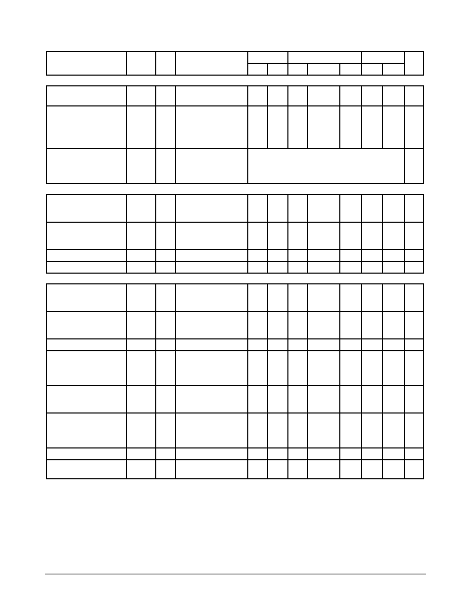
LOGIC DIAGRAM AND TRUTH TABLE
(1/4 OF DEVICE SHOWN)
BLOCK DIAGRAM
IN/OUT
CONTROL
OUT/IN
IN 4
CONTROL 4
IN 3
CONTROL 3
IN 2
CONTROL 2
IN 1
CONTROL 1
OUT 1
OUT 2
OUT 3
OUT 4
13
1
5
4
6
8
12
11
2
3
9
10
V
DD
= PIN 14
V
SS
= PIN 7
Control
Switch
0 = V
SS
OFF
1 = V
DD
ON
Logic Diagram Restrictions
V
SS
V
in
V
DD
V
SS
V
out
V
DD
CIRCUIT SCHEMATIC
(1/4 OF CIRCUIT SHOWN)
V
DD
V
DD
V
DD
V
DD
V
DD
V
DD
V
DD
V
SS
V
SS
V
SS
300
CMOS
INPUT
MC14066B
http://onsemi.com
3
ŒŒŒŒŒŒŒŒŒŒŒŒŒŒŒŒŒŒŒŒŒŒŒŒŒŒŒŒŒŒŒŒŒ
ŒŒŒŒŒŒŒŒŒŒŒŒŒŒŒŒŒŒŒŒŒŒŒŒŒŒŒŒŒŒŒŒŒ
ELECTRICAL CHARACTERISTICS
ŒŒŒŒŒŒŒŒ
ŒŒŒŒŒŒŒŒ
ŒŒŒŒ
ŒŒŒŒ
ŒŒ
ŒŒ
ŒŒŒŒŒŒŒ
ŒŒŒŒŒŒŒ
ŒŒŒŒŒ
ŒŒŒŒŒ
≠ 55
_
C
ŒŒŒŒŒŒŒ
ŒŒŒŒŒŒŒ
25
_
C
ŒŒŒŒŒ
ŒŒŒŒŒ
125
_
C
ŒŒ
ŒŒ
ŒŒŒŒŒŒŒŒ
ŒŒŒŒŒŒŒŒ
Characteristic
ŒŒŒŒ
ŒŒŒŒ
Symbol
ŒŒ
ŒŒ
V
DD
ŒŒŒŒŒŒŒ
ŒŒŒŒŒŒŒ
Test Conditions
ŒŒŒ
ŒŒŒ
Min
ŒŒŒ
ŒŒŒ
Max
ŒŒ
ŒŒ
Min
ŒŒŒŒ
ŒŒŒŒ
Typ
(4.)
ŒŒŒ
ŒŒŒ
Max
ŒŒŒ
ŒŒŒ
Min
ŒŒŒ
ŒŒŒ
Max
ŒŒ
ŒŒ
Unit
ŒŒŒŒŒŒŒŒŒŒŒŒŒŒŒŒŒŒŒŒŒŒŒŒŒŒŒŒŒŒŒŒŒ
ŒŒŒŒŒŒŒŒŒŒŒŒŒŒŒŒŒŒŒŒŒŒŒŒŒŒŒŒŒŒŒŒŒ
SUPPLY REQUIREMENTS (Voltages Referenced to V
EE
)
ŒŒŒŒŒŒŒŒ
ŒŒŒŒŒŒŒŒ
Power Supply Voltage
Range
ŒŒŒŒ
ŒŒŒŒ
V
DD
ŒŒ
ŒŒ
--
ŒŒŒŒŒŒŒ
ŒŒŒŒŒŒŒ
ŒŒŒ
ŒŒŒ
3.0
ŒŒŒ
ŒŒŒ
18
ŒŒ
ŒŒ
3.0
ŒŒŒŒ
ŒŒŒŒ
--
ŒŒŒ
ŒŒŒ
18
ŒŒŒ
ŒŒŒ
3.0
ŒŒŒ
ŒŒŒ
18
ŒŒ
ŒŒ
V
ŒŒŒŒŒŒŒŒ
Œ
ŒŒŒŒŒŒ
Œ
Œ
ŒŒŒŒŒŒ
Œ
Œ
ŒŒŒŒŒŒ
Œ
ŒŒŒŒŒŒŒŒ
Quiescent Current Per
Package
ŒŒŒŒ
Œ
ŒŒ
Œ
Œ
ŒŒ
Œ
Œ
ŒŒ
Œ
ŒŒŒŒ
I
DD
ŒŒ
ŒŒ
ŒŒ
ŒŒ
ŒŒ
5.0
10
15
ŒŒŒŒŒŒŒ
Œ
ŒŒŒŒŒ
Œ
Œ
ŒŒŒŒŒ
Œ
Œ
ŒŒŒŒŒ
Œ
ŒŒŒŒŒŒŒ
Control Inputs:
V
in
= V
SS
or V
DD
,
Switch I/O: V
SS
v
V
I/O
v
V
DD
, and
V
switch
v
500 mV
(5.)
ŒŒŒ
Œ
Œ
Œ
Œ
Œ
Œ
Œ
Œ
Œ
ŒŒŒ
--
--
--
ŒŒŒ
Œ
Œ
Œ
Œ
Œ
Œ
Œ
Œ
Œ
ŒŒŒ
0.25
0.5
1.0
ŒŒ
ŒŒ
ŒŒ
ŒŒ
ŒŒ
--
--
--
ŒŒŒŒ
Œ
ŒŒ
Œ
Œ
ŒŒ
Œ
Œ
ŒŒ
Œ
ŒŒŒŒ
0.005
0.010
0.015
ŒŒŒ
Œ
Œ
Œ
Œ
Œ
Œ
Œ
Œ
Œ
ŒŒŒ
0.25
0.5
1.0
ŒŒŒ
Œ
Œ
Œ
Œ
Œ
Œ
Œ
Œ
Œ
ŒŒŒ
--
--
--
ŒŒŒ
Œ
Œ
Œ
Œ
Œ
Œ
Œ
Œ
Œ
ŒŒŒ
7.5
15
30
ŒŒ
ŒŒ
ŒŒ
ŒŒ
ŒŒ
µ
A
ŒŒŒŒŒŒŒŒ
Œ
ŒŒŒŒŒŒ
Œ
Œ
ŒŒŒŒŒŒ
Œ
ŒŒŒŒŒŒŒŒ
Total Supply Current
(Dynamic Plus Quiescent,
Per Package
ŒŒŒŒ
Œ
ŒŒ
Œ
Œ
ŒŒ
Œ
ŒŒŒŒ
I
D(AV)
ŒŒ
ŒŒ
ŒŒ
ŒŒ
5.0
10
15
ŒŒŒŒŒŒŒ
Œ
ŒŒŒŒŒ
Œ
Œ
ŒŒŒŒŒ
Œ
ŒŒŒŒŒŒŒ
T
A
= 25
_
C only The
channel component,
(V
in
≠ V
out
)/R
on
, is
not included.)
ŒŒŒŒŒŒŒŒŒŒŒŒŒŒŒ
Œ
ŒŒŒŒŒŒŒŒŒŒŒŒŒ
Œ
Œ
ŒŒŒŒŒŒŒŒŒŒŒŒŒ
Œ
ŒŒŒŒŒŒŒŒŒŒŒŒŒŒŒ
(0.07
µ
A/kHz) f + I
DD
Typical
(0.20
µ
A/kHz) f + I
DD
(0.36
µ
A/kHz) f + I
DD
ŒŒ
ŒŒ
ŒŒ
ŒŒ
µ
A
ŒŒŒŒŒŒŒŒŒŒŒŒŒŒŒŒŒŒŒŒŒŒŒŒŒŒŒŒŒŒŒŒŒ
ŒŒŒŒŒŒŒŒŒŒŒŒŒŒŒŒŒŒŒŒŒŒŒŒŒŒŒŒŒŒŒŒŒ
CONTROL INPUTS (Voltages Referenced to V
SS
)
ŒŒŒŒŒŒŒŒ
Œ
ŒŒŒŒŒŒ
Œ
ŒŒŒŒŒŒŒŒ
Low≠Level Input Voltage
ŒŒŒŒ
Œ
ŒŒ
Œ
ŒŒŒŒ
V
IL
ŒŒ
ŒŒ
ŒŒ
5.0
10
15
ŒŒŒŒŒŒŒ
Œ
ŒŒŒŒŒ
Œ
ŒŒŒŒŒŒŒ
R
on
= per spec,
I
off
= per spec
ŒŒŒ
Œ
Œ
Œ
ŒŒŒ
--
--
--
ŒŒŒ
Œ
Œ
Œ
ŒŒŒ
1.5
3.0
4.0
ŒŒ
ŒŒ
ŒŒ
--
--
--
ŒŒŒŒ
Œ
ŒŒ
Œ
ŒŒŒŒ
2.25
4.50
6.75
ŒŒŒ
Œ
Œ
Œ
ŒŒŒ
1.5
3.0
4.0
ŒŒŒ
Œ
Œ
Œ
ŒŒŒ
--
--
--
ŒŒŒ
Œ
Œ
Œ
ŒŒŒ
1.5
3.0
4.0
ŒŒ
ŒŒ
ŒŒ
V
ŒŒŒŒŒŒŒŒ
Œ
ŒŒŒŒŒŒ
Œ
Œ
ŒŒŒŒŒŒ
Œ
ŒŒŒŒŒŒŒŒ
High≠Level Input Voltage
ŒŒŒŒ
Œ
ŒŒ
Œ
Œ
ŒŒ
Œ
ŒŒŒŒ
V
IH
ŒŒ
ŒŒ
ŒŒ
ŒŒ
5.0
10
15
ŒŒŒŒŒŒŒ
Œ
ŒŒŒŒŒ
Œ
Œ
ŒŒŒŒŒ
Œ
ŒŒŒŒŒŒŒ
R
on
= per spec,
I
off
= per spec
ŒŒŒ
Œ
Œ
Œ
Œ
Œ
Œ
ŒŒŒ
3.5
7.0
11
ŒŒŒ
Œ
Œ
Œ
Œ
Œ
Œ
ŒŒŒ
--
--
--
ŒŒ
ŒŒ
ŒŒ
ŒŒ
3.5
7.0
11
ŒŒŒŒ
Œ
ŒŒ
Œ
Œ
ŒŒ
Œ
ŒŒŒŒ
2.75
5.50
8.25
ŒŒŒ
Œ
Œ
Œ
Œ
Œ
Œ
ŒŒŒ
--
--
--
ŒŒŒ
Œ
Œ
Œ
Œ
Œ
Œ
ŒŒŒ
3.5
7.0
11
ŒŒŒ
Œ
Œ
Œ
Œ
Œ
Œ
ŒŒŒ
--
--
--
ŒŒ
ŒŒ
ŒŒ
ŒŒ
V
ŒŒŒŒŒŒŒŒ
ŒŒŒŒŒŒŒŒ
Input Leakage Current
ŒŒŒŒ
ŒŒŒŒ
I
in
ŒŒ
ŒŒ
15
ŒŒŒŒŒŒŒ
ŒŒŒŒŒŒŒ
V
in
= 0 or V
DD
ŒŒŒ
ŒŒŒ
--
ŒŒŒ
ŒŒŒ
±
0.1
ŒŒ
ŒŒ
--
ŒŒŒŒ
ŒŒŒŒ
±
0.00001
ŒŒŒ
ŒŒŒ
±
0.1
ŒŒŒ
ŒŒŒ
--
ŒŒŒ
ŒŒŒ
±
1.0
ŒŒ
ŒŒ
µ
A
ŒŒŒŒŒŒŒŒ
ŒŒŒŒŒŒŒŒ
Input Capacitance
ŒŒŒŒ
ŒŒŒŒ
C
in
ŒŒ
ŒŒ
--
ŒŒŒŒŒŒŒ
ŒŒŒŒŒŒŒ
ŒŒŒ
ŒŒŒ
--
ŒŒŒ
ŒŒŒ
--
ŒŒ
ŒŒ
--
ŒŒŒŒ
ŒŒŒŒ
5.0
ŒŒŒ
ŒŒŒ
7.5
ŒŒŒ
ŒŒŒ
--
ŒŒŒ
ŒŒŒ
--
ŒŒ
ŒŒ
pF
ŒŒŒŒŒŒŒŒŒŒŒŒŒŒŒŒŒŒŒŒŒŒŒŒŒŒŒŒŒŒŒŒŒ
SWITCHES IN AND OUT (Voltages Referenced to V
SS
)
ŒŒŒŒŒŒŒŒ
Œ
ŒŒŒŒŒŒ
Œ
Œ
ŒŒŒŒŒŒ
Œ
ŒŒŒŒŒŒŒŒ
Recommended Peak≠to≠
Peak Voltage Into or Out
of the Switch
ŒŒŒŒ
Œ
ŒŒ
Œ
Œ
ŒŒ
Œ
ŒŒŒŒ
V
I/O
ŒŒ
ŒŒ
ŒŒ
ŒŒ
--
ŒŒŒŒŒŒŒ
Œ
ŒŒŒŒŒ
Œ
Œ
ŒŒŒŒŒ
Œ
ŒŒŒŒŒŒŒ
Channel On or Off
ŒŒŒ
Œ
Œ
Œ
Œ
Œ
Œ
ŒŒŒ
0
ŒŒŒ
Œ
Œ
Œ
Œ
Œ
Œ
ŒŒŒ
V
DD
ŒŒ
ŒŒ
ŒŒ
ŒŒ
0
ŒŒŒŒ
Œ
ŒŒ
Œ
Œ
ŒŒ
Œ
ŒŒŒŒ
--
ŒŒŒ
Œ
Œ
Œ
Œ
Œ
Œ
ŒŒŒ
V
DD
ŒŒŒ
Œ
Œ
Œ
Œ
Œ
Œ
ŒŒŒ
0
ŒŒŒ
Œ
Œ
Œ
Œ
Œ
Œ
ŒŒŒ
V
DD
ŒŒ
ŒŒ
ŒŒ
ŒŒ
V
p≠p
ŒŒŒŒŒŒŒŒ
Œ
ŒŒŒŒŒŒ
Œ
ŒŒŒŒŒŒŒŒ
Recommended Static or
Dynamic Voltage Across
the Switch (5.) (Figure 1)
ŒŒŒŒ
Œ
ŒŒ
Œ
ŒŒŒŒ
V
switch
ŒŒ
ŒŒ
ŒŒ
--
ŒŒŒŒŒŒŒ
Œ
ŒŒŒŒŒ
Œ
ŒŒŒŒŒŒŒ
Channel On
ŒŒŒ
Œ
Œ
Œ
ŒŒŒ
0
ŒŒŒ
Œ
Œ
Œ
ŒŒŒ
600
ŒŒ
ŒŒ
ŒŒ
0
ŒŒŒŒ
Œ
ŒŒ
Œ
ŒŒŒŒ
--
ŒŒŒ
Œ
Œ
Œ
ŒŒŒ
600
ŒŒŒ
Œ
Œ
Œ
ŒŒŒ
0
ŒŒŒ
Œ
Œ
Œ
ŒŒŒ
300
ŒŒ
ŒŒ
ŒŒ
mV
ŒŒŒŒŒŒŒŒ
ŒŒŒŒŒŒŒŒ
Output Offset Voltage
ŒŒŒŒ
ŒŒŒŒ
V
OO
ŒŒ
ŒŒ
--
ŒŒŒŒŒŒŒ
ŒŒŒŒŒŒŒ
V
in
= 0 V, No Load
ŒŒŒ
ŒŒŒ
--
ŒŒŒ
ŒŒŒ
--
ŒŒ
ŒŒ
--
ŒŒŒŒ
ŒŒŒŒ
10
ŒŒŒ
ŒŒŒ
--
ŒŒŒ
ŒŒŒ
--
ŒŒŒ
ŒŒŒ
--
ŒŒ
ŒŒ
µ
V
ŒŒŒŒŒŒŒŒ
Œ
ŒŒŒŒŒŒ
Œ
Œ
ŒŒŒŒŒŒ
Œ
ŒŒŒŒŒŒŒŒ
ON Resistance
ŒŒŒŒ
Œ
ŒŒ
Œ
Œ
ŒŒ
Œ
ŒŒŒŒ
R
on
ŒŒ
ŒŒ
ŒŒ
ŒŒ
5.0
10
15
ŒŒŒŒŒŒŒ
Œ
ŒŒŒŒŒ
Œ
Œ
ŒŒŒŒŒ
Œ
ŒŒŒŒŒŒŒ
V
switch
v
500 mV
(5.)
,
V
in
= V
IL
or V
IH
(Control), and V
in
=
0 to V
DD
(Switch)
ŒŒŒ
Œ
Œ
Œ
Œ
Œ
Œ
ŒŒŒ
--
--
--
ŒŒŒ
Œ
Œ
Œ
Œ
Œ
Œ
ŒŒŒ
800
400
220
ŒŒ
ŒŒ
ŒŒ
ŒŒ
--
--
--
ŒŒŒŒ
Œ
ŒŒ
Œ
Œ
ŒŒ
Œ
ŒŒŒŒ
250
120
80
ŒŒŒ
Œ
Œ
Œ
Œ
Œ
Œ
ŒŒŒ
1050
500
280
ŒŒŒ
Œ
Œ
Œ
Œ
Œ
Œ
ŒŒŒ
--
--
--
ŒŒŒ
Œ
Œ
Œ
Œ
Œ
Œ
ŒŒŒ
1200
520
300
ŒŒ
ŒŒ
ŒŒ
ŒŒ
ŒŒŒŒŒŒŒŒ
Œ
ŒŒŒŒŒŒ
Œ
ŒŒŒŒŒŒŒŒ
ON Resistance Between
Any Two Channels
in the Same Package
ŒŒŒŒ
Œ
ŒŒ
Œ
ŒŒŒŒ
R
on
ŒŒ
ŒŒ
ŒŒ
5.0
10
15
ŒŒŒŒŒŒŒ
Œ
ŒŒŒŒŒ
Œ
ŒŒŒŒŒŒŒ
ŒŒŒ
Œ
Œ
Œ
ŒŒŒ
--
--
--
ŒŒŒ
Œ
Œ
Œ
ŒŒŒ
70
50
45
ŒŒ
ŒŒ
ŒŒ
--
--
--
ŒŒŒŒ
Œ
ŒŒ
Œ
ŒŒŒŒ
25
10
10
ŒŒŒ
Œ
Œ
Œ
ŒŒŒ
70
50
45
ŒŒŒ
Œ
Œ
Œ
ŒŒŒ
--
--
--
ŒŒŒ
Œ
Œ
Œ
ŒŒŒ
135
95
65
ŒŒ
ŒŒ
ŒŒ
ŒŒŒŒŒŒŒŒ
Œ
ŒŒŒŒŒŒ
Œ
Œ
ŒŒŒŒŒŒ
Œ
ŒŒŒŒŒŒŒŒ
Off≠Channel Leakage
Current (Figure 6)
ŒŒŒŒ
Œ
ŒŒ
Œ
Œ
ŒŒ
Œ
ŒŒŒŒ
I
off
ŒŒ
ŒŒ
ŒŒ
ŒŒ
15
ŒŒŒŒŒŒŒ
Œ
ŒŒŒŒŒ
Œ
Œ
ŒŒŒŒŒ
Œ
ŒŒŒŒŒŒŒ
V
in
= V
IL
or V
IH
(Control) Channel to
Channel or Any One
Channel
ŒŒŒ
Œ
Œ
Œ
Œ
Œ
Œ
ŒŒŒ
--
ŒŒŒ
Œ
Œ
Œ
Œ
Œ
Œ
ŒŒŒ
±
100
ŒŒ
ŒŒ
ŒŒ
ŒŒ
--
ŒŒŒŒ
Œ
ŒŒ
Œ
Œ
ŒŒ
Œ
ŒŒŒŒ
±
0.05
ŒŒŒ
Œ
Œ
Œ
Œ
Œ
Œ
ŒŒŒ
±
100
ŒŒŒ
Œ
Œ
Œ
Œ
Œ
Œ
ŒŒŒ
--
ŒŒŒ
Œ
Œ
Œ
Œ
Œ
Œ
ŒŒŒ
±
1000
ŒŒ
ŒŒ
ŒŒ
ŒŒ
nA
ŒŒŒŒŒŒŒŒ
ŒŒŒŒŒŒŒŒ
Capacitance, Switch I/O
ŒŒŒŒ
ŒŒŒŒ
C
I/O
ŒŒ
ŒŒ
--
ŒŒŒŒŒŒŒ
ŒŒŒŒŒŒŒ
Switch Off
ŒŒŒ
ŒŒŒ
--
ŒŒŒ
ŒŒŒ
--
ŒŒ
ŒŒ
--
ŒŒŒŒ
ŒŒŒŒ
10
ŒŒŒ
ŒŒŒ
15
ŒŒŒ
ŒŒŒ
--
ŒŒŒ
ŒŒŒ
--
ŒŒ
ŒŒ
pF
ŒŒŒŒŒŒŒŒ
Œ
ŒŒŒŒŒŒ
Œ
ŒŒŒŒŒŒŒŒ
Capacitance, Feedthrough
(Switch Off)
ŒŒŒŒ
Œ
ŒŒ
Œ
ŒŒŒŒ
C
I/O
ŒŒ
ŒŒ
ŒŒ
--
--
ŒŒŒŒŒŒŒ
Œ
ŒŒŒŒŒ
Œ
ŒŒŒŒŒŒŒ
ŒŒŒ
Œ
Œ
Œ
ŒŒŒ
--
ŒŒŒ
Œ
Œ
Œ
ŒŒŒ
--
ŒŒ
ŒŒ
ŒŒ
--
ŒŒŒŒ
Œ
ŒŒ
Œ
ŒŒŒŒ
0.47
ŒŒŒ
Œ
Œ
Œ
ŒŒŒ
--
ŒŒŒ
Œ
Œ
Œ
ŒŒŒ
--
ŒŒŒ
Œ
Œ
Œ
ŒŒŒ
--
ŒŒ
ŒŒ
ŒŒ
pF
4. Data labeled "Typ" is not to be used for design purposes, but is intended as an indication of the IC's potential performance.
5. For voltage drops across the switch (
V
switch
) > 600 mV ( > 300 mV at high temperature), excessive V
DD
current may be drawn; i.e. the
current out of the switch may contain both V
DD
and switch input components. The reliability of the device will be unaffected unless the
Maximum Ratings are exceeded. (See first page of this data sheet.)
MC14066B
http://onsemi.com
4
ŒŒŒŒŒŒŒŒŒŒŒŒŒŒŒŒŒŒŒŒŒŒŒŒŒŒŒŒŒŒŒŒŒ
ŒŒŒŒŒŒŒŒŒŒŒŒŒŒŒŒŒŒŒŒŒŒŒŒŒŒŒŒŒŒŒŒŒ
ELECTRICAL CHARACTERISTICS
(6.)
(C
L
= 50 pF, T
A
= 25
_
C unless otherwise noted.)
ŒŒŒŒŒŒŒŒŒŒŒŒŒŒŒŒ
ŒŒŒŒŒŒŒŒŒŒŒŒŒŒŒŒ
Characteristic
ŒŒŒŒ
ŒŒŒŒ
Symbol
ŒŒŒŒ
ŒŒŒŒ
V
DD
Vdc
ŒŒŒŒ
ŒŒŒŒ
Min
ŒŒŒŒ
ŒŒŒŒ
Typ
(7.)
ŒŒŒŒ
ŒŒŒŒ
Max
ŒŒŒ
ŒŒŒ
Unit
ŒŒŒŒŒŒŒŒŒŒŒŒŒŒŒŒ
Œ
ŒŒŒŒŒŒŒŒŒŒŒŒŒŒ
Œ
Œ
ŒŒŒŒŒŒŒŒŒŒŒŒŒŒ
Œ
Œ
ŒŒŒŒŒŒŒŒŒŒŒŒŒŒ
Œ
ŒŒŒŒŒŒŒŒŒŒŒŒŒŒŒŒ
Propagation Delay Times
V
SS
= 0 Vdc
Input to Output (R
L
= 10 k
)
t
PLH
, t
PHL
= (0.17 ns/pF) C
L
+ 15.5 ns
t
PLH
, t
PHL
= (0.08 ns/pF) C
L
+ 6.0 ns
t
PLH
, t
PHL
= (0.06 ns/pF) C
L
+ 4.0 ns
ŒŒŒŒ
Œ
ŒŒ
Œ
Œ
ŒŒ
Œ
Œ
ŒŒ
Œ
ŒŒŒŒ
t
PLH
, t
PHL
ŒŒŒŒ
Œ
ŒŒ
Œ
Œ
ŒŒ
Œ
Œ
ŒŒ
Œ
ŒŒŒŒ
5.0
10
15
ŒŒŒŒ
Œ
ŒŒ
Œ
Œ
ŒŒ
Œ
Œ
ŒŒ
Œ
ŒŒŒŒ
--
--
--
ŒŒŒŒ
Œ
ŒŒ
Œ
Œ
ŒŒ
Œ
Œ
ŒŒ
Œ
ŒŒŒŒ
20
10
7.0
ŒŒŒŒ
Œ
ŒŒ
Œ
Œ
ŒŒ
Œ
Œ
ŒŒ
Œ
ŒŒŒŒ
40
20
15
ŒŒŒ
Œ
Œ
Œ
Œ
Œ
Œ
Œ
Œ
Œ
ŒŒŒ
ns
ŒŒŒŒŒŒŒŒŒŒŒŒŒŒŒŒ
Œ
ŒŒŒŒŒŒŒŒŒŒŒŒŒŒ
Œ
Œ
ŒŒŒŒŒŒŒŒŒŒŒŒŒŒ
Œ
ŒŒŒŒŒŒŒŒŒŒŒŒŒŒŒŒ
Control to Output (R
L
= 1 k
) (Figure 2)
Output "1" to High Impedance
ŒŒŒŒ
Œ
ŒŒ
Œ
Œ
ŒŒ
Œ
ŒŒŒŒ
t
PHZ
ŒŒŒŒ
Œ
ŒŒ
Œ
Œ
ŒŒ
Œ
ŒŒŒŒ
5.0
10
15
ŒŒŒŒ
Œ
ŒŒ
Œ
Œ
ŒŒ
Œ
ŒŒŒŒ
--
--
--
ŒŒŒŒ
Œ
ŒŒ
Œ
Œ
ŒŒ
Œ
ŒŒŒŒ
40
35
30
ŒŒŒŒ
Œ
ŒŒ
Œ
Œ
ŒŒ
Œ
ŒŒŒŒ
80
70
60
ŒŒŒ
Œ
Œ
Œ
Œ
Œ
Œ
ŒŒŒ
ns
ŒŒŒŒŒŒŒŒŒŒŒŒŒŒŒŒ
Œ
ŒŒŒŒŒŒŒŒŒŒŒŒŒŒ
Œ
ŒŒŒŒŒŒŒŒŒŒŒŒŒŒŒŒ
Output "0" to High Impedance
ŒŒŒŒ
Œ
ŒŒ
Œ
ŒŒŒŒ
t
PLZ
ŒŒŒŒ
Œ
ŒŒ
Œ
ŒŒŒŒ
5.0
10
15
ŒŒŒŒ
Œ
ŒŒ
Œ
ŒŒŒŒ
--
--
--
ŒŒŒŒ
Œ
ŒŒ
Œ
ŒŒŒŒ
40
35
30
ŒŒŒŒ
Œ
ŒŒ
Œ
ŒŒŒŒ
80
70
60
ŒŒŒ
Œ
Œ
Œ
ŒŒŒ
ns
ŒŒŒŒŒŒŒŒŒŒŒŒŒŒŒŒ
Œ
ŒŒŒŒŒŒŒŒŒŒŒŒŒŒ
Œ
Œ
ŒŒŒŒŒŒŒŒŒŒŒŒŒŒ
Œ
ŒŒŒŒŒŒŒŒŒŒŒŒŒŒŒŒ
High Impedance to Output "1"
ŒŒŒŒ
Œ
ŒŒ
Œ
Œ
ŒŒ
Œ
ŒŒŒŒ
t
PZH
ŒŒŒŒ
Œ
ŒŒ
Œ
Œ
ŒŒ
Œ
ŒŒŒŒ
5.0
10
15
ŒŒŒŒ
Œ
ŒŒ
Œ
Œ
ŒŒ
Œ
ŒŒŒŒ
--
--
--
ŒŒŒŒ
Œ
ŒŒ
Œ
Œ
ŒŒ
Œ
ŒŒŒŒ
60
20
15
ŒŒŒŒ
Œ
ŒŒ
Œ
Œ
ŒŒ
Œ
ŒŒŒŒ
120
40
30
ŒŒŒ
Œ
Œ
Œ
Œ
Œ
Œ
ŒŒŒ
ns
ŒŒŒŒŒŒŒŒŒŒŒŒŒŒŒŒ
Œ
ŒŒŒŒŒŒŒŒŒŒŒŒŒŒ
Œ
ŒŒŒŒŒŒŒŒŒŒŒŒŒŒŒŒ
High Impedance to Output "0"
ŒŒŒŒ
Œ
ŒŒ
Œ
ŒŒŒŒ
t
PZL
ŒŒŒŒ
Œ
ŒŒ
Œ
ŒŒŒŒ
5.0
10
15
ŒŒŒŒ
Œ
ŒŒ
Œ
ŒŒŒŒ
--
--
--
ŒŒŒŒ
Œ
ŒŒ
Œ
ŒŒŒŒ
60
20
15
ŒŒŒŒ
Œ
ŒŒ
Œ
ŒŒŒŒ
120
40
30
ŒŒŒ
Œ
Œ
Œ
ŒŒŒ
ns
ŒŒŒŒŒŒŒŒŒŒŒŒŒŒŒŒ
Œ
ŒŒŒŒŒŒŒŒŒŒŒŒŒŒ
Œ
ŒŒŒŒŒŒŒŒŒŒŒŒŒŒŒŒ
Second Harmonic Distortion
V
SS
= ≠ 5 Vdc
(V
in
= 1.77 Vdc, RMS Centered @ 0.0 Vdc,
R
L
= 10 k
, f = 1.0 kHz)
ŒŒŒŒ
Œ
ŒŒ
Œ
ŒŒŒŒ
--
ŒŒŒŒ
Œ
ŒŒ
Œ
ŒŒŒŒ
5.0
ŒŒŒŒ
Œ
ŒŒ
Œ
ŒŒŒŒ
--
ŒŒŒŒ
Œ
ŒŒ
Œ
ŒŒŒŒ
0.1
ŒŒŒŒ
Œ
ŒŒ
Œ
ŒŒŒŒ
--
ŒŒŒ
Œ
Œ
Œ
ŒŒŒ
%
ŒŒŒŒŒŒŒŒŒŒŒŒŒŒŒŒ
Œ
ŒŒŒŒŒŒŒŒŒŒŒŒŒŒ
Œ
Œ
ŒŒŒŒŒŒŒŒŒŒŒŒŒŒ
Œ
ŒŒŒŒŒŒŒŒŒŒŒŒŒŒŒŒ
Bandwidth (Switch ON) (Figure 3)
V
SS
= ≠ 5 Vdc
(R
L
= 1 k
, 20 Log (V
out
/V
in
) = ≠ 3 dB, C
L
= 50 pF,
V
in
= 5 V
p≠p
)
ŒŒŒŒ
Œ
ŒŒ
Œ
Œ
ŒŒ
Œ
ŒŒŒŒ
--
ŒŒŒŒ
Œ
ŒŒ
Œ
Œ
ŒŒ
Œ
ŒŒŒŒ
5.0
ŒŒŒŒ
Œ
ŒŒ
Œ
Œ
ŒŒ
Œ
ŒŒŒŒ
--
ŒŒŒŒ
Œ
ŒŒ
Œ
Œ
ŒŒ
Œ
ŒŒŒŒ
65
ŒŒŒŒ
Œ
ŒŒ
Œ
Œ
ŒŒ
Œ
ŒŒŒŒ
--
ŒŒŒ
Œ
Œ
Œ
Œ
Œ
Œ
ŒŒŒ
MHz
ŒŒŒŒŒŒŒŒŒŒŒŒŒŒŒŒ
ŒŒŒŒŒŒŒŒŒŒŒŒŒŒŒŒ
Feedthrough Attenuation (Switch OFF)
V
SS
= ≠ 5 Vdc
(V
in
= 5 V
p≠p
, R
L
= 1 k
, f
in
= 1.0 MHz) (Figure 3)
ŒŒŒŒ
ŒŒŒŒ
--
ŒŒŒŒ
ŒŒŒŒ
5.0
ŒŒŒŒ
ŒŒŒŒ
--
ŒŒŒŒ
ŒŒŒŒ
≠ 50
ŒŒŒŒ
ŒŒŒŒ
--
ŒŒŒ
ŒŒŒ
dB
ŒŒŒŒŒŒŒŒŒŒŒŒŒŒŒŒ
Œ
ŒŒŒŒŒŒŒŒŒŒŒŒŒŒ
Œ
Œ
ŒŒŒŒŒŒŒŒŒŒŒŒŒŒ
Œ
ŒŒŒŒŒŒŒŒŒŒŒŒŒŒŒŒ
Channel Separation (Figure 4)
V
SS
= ≠ 5 Vdc
(V
in
= 5 V
p≠p
, R
L
= 1 k
, f
in
= 8.0 MHz)
(Switch A ON, Switch B OFF)
ŒŒŒŒ
Œ
ŒŒ
Œ
Œ
ŒŒ
Œ
ŒŒŒŒ
--
ŒŒŒŒ
Œ
ŒŒ
Œ
Œ
ŒŒ
Œ
ŒŒŒŒ
5.0
ŒŒŒŒ
Œ
ŒŒ
Œ
Œ
ŒŒ
Œ
ŒŒŒŒ
--
ŒŒŒŒ
Œ
ŒŒ
Œ
Œ
ŒŒ
Œ
ŒŒŒŒ
≠ 50
ŒŒŒŒ
Œ
ŒŒ
Œ
Œ
ŒŒ
Œ
ŒŒŒŒ
--
ŒŒŒ
Œ
Œ
Œ
Œ
Œ
Œ
ŒŒŒ
dB
ŒŒŒŒŒŒŒŒŒŒŒŒŒŒŒŒ
Œ
ŒŒŒŒŒŒŒŒŒŒŒŒŒŒ
Œ
ŒŒŒŒŒŒŒŒŒŒŒŒŒŒŒŒ
Crosstalk, Control Input to Signal Output (Figure 5)
V
SS
= ≠ 5 Vdc
(R
1
= 1 k
, R
L
= 10 k
, Control t
TLH
= t
THL
= 20 ns)
ŒŒŒŒ
Œ
ŒŒ
Œ
ŒŒŒŒ
--
ŒŒŒŒ
Œ
ŒŒ
Œ
ŒŒŒŒ
5.0
ŒŒŒŒ
Œ
ŒŒ
Œ
ŒŒŒŒ
--
ŒŒŒŒ
Œ
ŒŒ
Œ
ŒŒŒŒ
300
ŒŒŒŒ
Œ
ŒŒ
Œ
ŒŒŒŒ
--
ŒŒŒ
Œ
Œ
Œ
ŒŒŒ
mV
p≠p
6. The formulas given are for the typical characteristics only at 25
_
C.
7. Data labelled "Typ" is not to be used for design purposes but is intended as an indication of the IC's potential performance.
MC14066B
http://onsemi.com
5
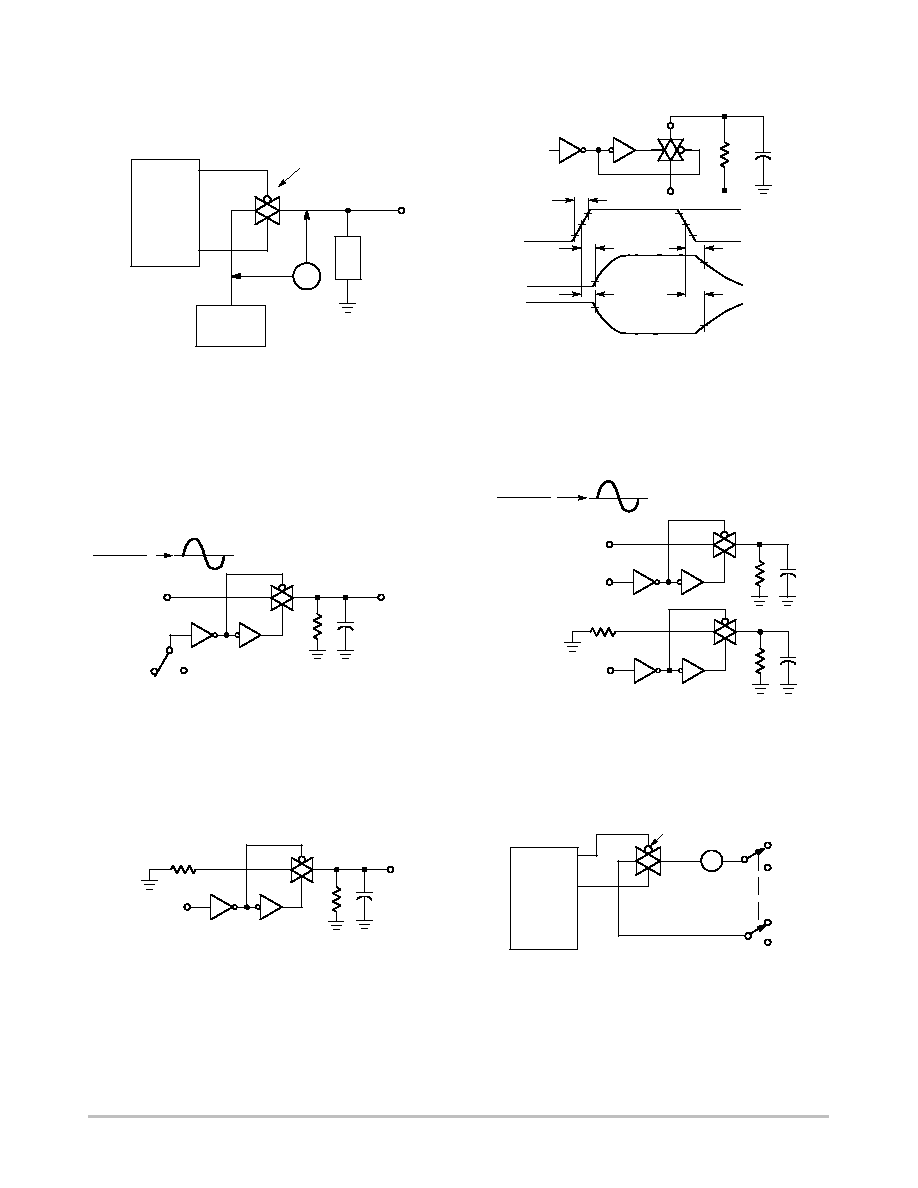
TEST CIRCUITS
Figure 1.
V Across Switch
Figure 2. Turn≠On Delay Time Test Circuit
and Waveforms
Figure 3. Bandwidth and
Feedthrough Attenuation
Figure 4. Channel Separation
Figure 5. Crosstalk,
Control to Output
Figure 6. Off Channel Leakage
CONTROL
SECTION
OF IC
SOURCE
V
LOAD
ON SWITCH
V
out
V
out
V
C
V
C
V
out
V
in
R
L
C
L
20 ns
V
DD
V
SS
90%
50%
10%
t
PZH
t
PHZ
t
PZL
t
PLZ
10%
90%
10%
V
x
V
out
C
L
R
L
V
DD
V
SS
V
C
V
in
V
DD
≠ V
SS
2
V
DD
≠ V
SS
2
V
in
V
DD
V
SS
R
L
C
L
R
L
C
L
V
in
1 k
V
out
R
L
C
L
= 50 pF
V
C
= ≠ 5.0 V TO + 5.0 V SWING
V
C
= V
DD
FOR BANDWIDTH TEST
V
C
= V
SS
FOR FEEDTHROUGH TEST
OFF CHANNEL UNDER TEST
V
DD
V
SS
V
SS
V
DD
A
CONTROL
SECTION
OF IC
90%
V
in
= V
DD
V
x
= V
SS
V
in
= V
SS
V
x
= V
DD
10 k