 | –≠–ª–µ–∫—Ç—Ä–æ–Ω–Ω—ã–π –∫–æ–º–ø–æ–Ω–µ–Ω—Ç: 74273 | –°–∫–∞—á–∞—Ç—å:  PDF PDF  ZIP ZIP |
©
Semiconductor Components Industries, LLC, 1999
December, 1999 ≠ Rev. 6
1
Publication Order Number:
SN74LS273/D
SN74LS273
Octal D Flip-Flop
with Clear
The SN74LS273 is a high-speed 8-Bit Register. The register
consists of eight D-Type Flip-Flops with a Common Clock and an
asynchronous active LOW Master Reset. This device is supplied in a
20-pin package featuring 0.3 inch lead spacing.
∑
8-Bit High Speed Register
∑
Parallel Register
∑
Common Clock and Master Reset
∑
Input Clamp Diodes Limit High-Speed Termination Effects
GUARANTEED OPERATING RANGES
Symbol
Parameter
Min
Typ
Max
Unit
V
CC
Supply Voltage
4.75
5.0
5.25
V
T
A
Operating Ambient
Temperature Range
0
25
70
∞
C
I
OH
Output Current ≠ High
≠ 0.4
mA
I
OL
Output Current ≠ Low
8.0
mA
LOW
POWER
SCHOTTKY
Device
Package
Shipping
ORDERING INFORMATION
SN74LS273N
16 Pin DIP
1440 Units/Box
SN74LS273DW
16 Pin
SOIC
DW SUFFIX
CASE 751D
http://onsemi.com
2500/Tape & Reel
PLASTIC
N SUFFIX
CASE 738
20
1
20
1
SN74LS273
http://onsemi.com
2
18
17
16
15
14
13
1
2
3
4
5
6
7
20
19
8
V
CC
MR
Q
7
D
7
D
6
Q
6
D
5
Q
5
D
4
Q
0
D
0
D
1
Q
1
Q
2
D
2
D
3
9
10
Q
3
GND
12
11
Q
4
CP
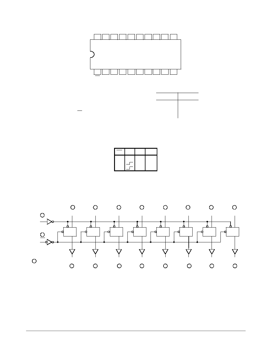
CONNECTION DIAGRAM DIP (TOP VIEW)
Clock (Active HIGH Going Edge) Input
Data Inputs
Master Reset (Active LOW) Input
Register Outputs
CP
D
0
≠ D
7
MR
Q
0
≠ Q
7
0.5 U.L.
0.5 U.L.
0.5 U.L.
10 U.L.
0.25 U.L.
0.25 U.L.
0.25 U.L.
5 U.L.
NOTES:
a) 1 TTL Unit Load (U.L.) = 40
mA HIGH/1.6 mA LOW.
HIGH
LOW
(Note a)
LOADING
PIN NAMES
TRUTH TABLE
MR
CP
D
x
Q
x
L
X
X
L
H
H
H
H
L
L
H = HIGH Logic Level
L = LOW Logic Level
X = Immaterial
LOGIC DIAGRAM
CP
MR
D
0
D
1
D
2
D
3
D
4
D
5
D
6
D
7
Q
0
Q
1
Q
2
Q
3
Q
4
Q
5
Q
6
Q
7
CP D
CD Q
CP D
CD Q
CP D
CD Q
CP D
CD Q
CP D
CD Q
CP D
CD Q
CP D
CD Q
CP D
CD Q
14
1
2
6
7
3
8
4
5
9
11
12
13
15
V
CC
= PIN 20
GND = PIN 10
= PIN NUMBERS
17
18
16
19
SN74LS273
http://onsemi.com
3
FUNCTIONAL DESCRIPTION
The SN74LS273 is an 8-Bit Parallel Register with a
common Clock and common Master Reset.
When the MR input is LOW, the Q outputs are LOW,
independent of the other inputs. Information meeting the
setup and hold time requirements of the D inputs is
transferred to the Q outputs on the LOW-to-HIGH transition
of the clock input.
DC CHARACTERISTICS OVER OPERATING TEMPERATURE RANGE
(unless otherwise specified)
Limits
Symbol
Parameter
Min
Typ
Max
Unit
Test Conditions
V
IH
Input HIGH Voltage
2.0
V
Guaranteed Input HIGH Voltage for
All Inputs
V
IL
Input LOW Voltage
0.8
V
Guaranteed Input LOW Voltage for
All Inputs
V
IK
Input Clamp Diode Voltage
≠ 0.65
≠ 1.5
V
V
CC
= MIN, I
IN
= ≠ 18 mA
V
OH
Output HIGH Voltage
2.7
3.5
V
V
CC
= MIN, I
OH
= MAX, V
IN
= V
IH
or V
IL
per Truth Table
V
O
Output LOW Voltage
0.25
0.4
V
I
OL
= 4.0 mA
V
CC
= V
CC
MIN,
V
IN
= V
IL
or V
IH
V
OL
Output LOW Voltage
0.35
0.5
V
I
OL
= 8.0 mA
V
IN
= V
IL
or V
IH
per Truth Table
I
Input HIGH Current
20
µ
A
V
CC
= MAX, V
IN
= 2.7 V
I
IH
Input HIGH Current
0.1
mA
V
CC
= MAX, V
IN
= 7.0 V
I
IL
Input LOW Current
≠ 0.4
mA
V
CC
= MAX, V
IN
= 0.4 V
I
OS
Short Circuit Current (Note 1)
≠ 20
≠ 100
mA
V
CC
= MAX
I
CC
Power Supply Current
27
mA
V
CC
= MAX
Note 1: Not more than one output should be shorted at a time, nor for more than 1 second.
AC CHARACTERISTICS
(T
A
= 25
∞
C, V
CC
= 5.0 V)
Limits
Symbol
Parameter
Min
Typ
Max
Unit
Test Conditions
f
MAX
Maximum Input Clock Frequency
30
40
MHz
Figure 1
t
PHL
Propagation Delay, MR to Q Output
18
27
ns
Figure 2
t
PLH
t
PHL
Propagation Delay, Clock to Output
17
18
27
27
ns
Figure 1
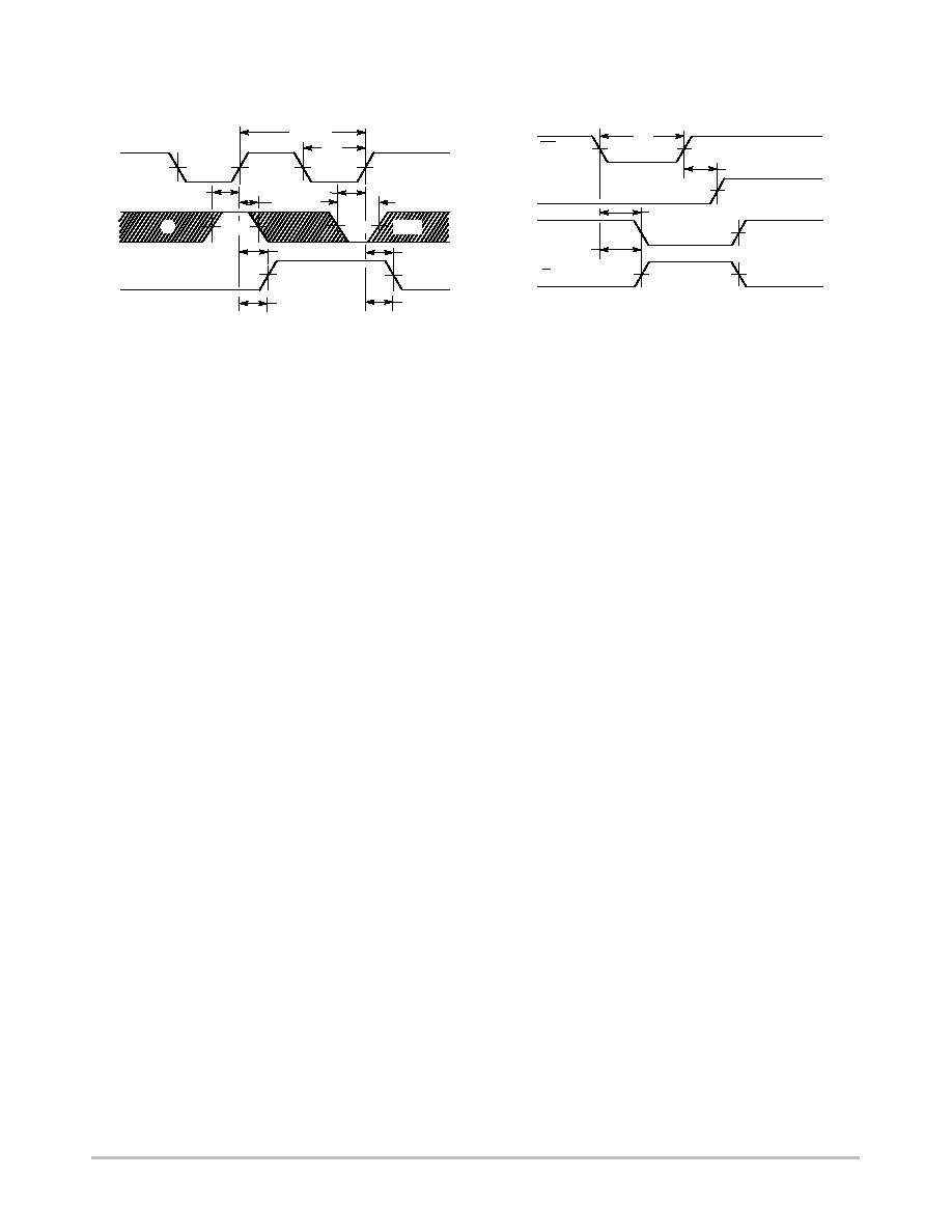
AC SETUP REQUIREMENTS
(T
A
= 25
∞
C, V
CC
= 5.0 V)
Limits
Symbol
Parameter
Min
Typ
Max
Unit
Test Conditions
t
w
Pulse Width, Clock or Clear
20
ns
Figure 1
t
s
Data Setup Time
20
ns
Figure 1
t
h
Hold Time
5.0
ns
Figure 1
t
rec
Recovery Time
25
ns
Figure 2
SN74LS273
http://onsemi.com
4
1.3 V
*The shaded areas indicate when the input is permitted to
*
change for predictable output performance.
1.3 V
1.3 V
1.3 V
1.3 V
1.3 V
CP
D
Q
n
t
s
(H)
t
h
(H)
t
s
(L)
t
h
(L)
1/f max
t
PLH
t
PLH
t
PHL
t
PHL
MR
CP
Q
n
Q
n
1.3 V
1.3 V
1.3 V
1.3 V
1.3 V
1.3 V
t
rec
t
PHL
t
PLH
t
W
1.3 V
1.3 V
1.3 V
*
t
W
Figure 1. Clock to Output Delays, Clock Pulse Width,
Frequency, Setup and Hold Times Data to Clock
Figure 2. Master Reset to Output Delay, Master Reset
Pulse Width, and Master Reset Recovery Time
AC WAVEFORMS
DEFINITION OF TERMS
SETUP TIME (t
s
) -- is defined as the minimum time
required for the correct logic level to be present at the logic
input prior to the clock transition from LOW-to-HIGH in
order to be recognized and transferred to the outputs.
HOLD TIME (t
h
) -- is defined as the minimum time
following the clock transition from LOW-to-HIGH that the
logic level must be maintained at the input in order to ensure
continued recognition. A negative HOLD TIME indicates
that the correct logic level may be released prior to the clock
transition from LOW-to-HIGH and still be recognized.
RECOVERY TIME (t
rec
) -- is defined as the minimum time
required between the end of the reset pulse and the clock
transition from LOW-to-HIGH in order to recognize and
transfer HIGH data to the Q outputs.

SN74LS273
http://onsemi.com
5
PACKAGE DIMENSIONS
N SUFFIX
PLASTIC PACKAGE
CASE 738≠03
ISSUE E
NOTES:
1. DIMENSIONING AND TOLERANCING PER ANSI
Y14.5M, 1982.
2. CONTROLLING DIMENSION: INCH.
3. DIMENSION L TO CENTER OF LEAD WHEN
FORMED PARALLEL.
4. DIMENSION B DOES NOT INCLUDE MOLD
FLASH.
M
L
J
20 PL
M
B
M
0.25 (0.010)
T
DIM
MIN
MAX
MIN
MAX
MILLIMETERS
INCHES
A
25.66
27.17
1.010
1.070
B
6.10
6.60
0.240
0.260
C
3.81
4.57
0.150
0.180
D
0.39
0.55
0.015
0.022
G
2.54 BSC
0.100 BSC
J
0.21
0.38
0.008
0.015
K
2.80
3.55
0.110
0.140
L
7.62 BSC
0.300 BSC
M
0
15
0
15
N
0.51
1.01
0.020
0.040
_
_
_
_
E
1.27
1.77
0.050
0.070
1
11
10
20
≠A≠
SEATING
PLANE
K
N
F
G
D
20 PL
≠T≠
M
A
M
0.25 (0.010)
T
E
B
C
F
1.27 BSC
0.050 BSC