©
Semiconductor Components Industries, LLC, 2001
December, 2001 ≠ Rev. 6
1
Publication Order Number:
CS4192/D
CS4192
Single Air-Core Gauge
Driver
The CS4192 is a monolithic BiCMOS integrated circuit used to
translate a digital 10≠bit word from a microprocessor/microcontroller
to complementary DC outputs. The DC outputs drive an air≠core
meter commonly used in vehicle instrument panels. The 10 bits of data
are used to linearly control the quadrature coils of the meter directly
with a 0.35
∞
resolution and
±
1.2
∞
accuracy over the full 360
∞
range of
the gauge. The interface from the microcontroller is by a Serial
Peripheral Interface (SPI) compatible serial connection using up to a
2.0 MHz shift clock rate.
The digital code, which is directly proportional to the desired gauge
pointer deflection, is shifted into a DAC and multiplexer. These two
blocks provide a tangential conversion function to change the digital
data into the appropriate DC coil voltage for the angle demanded. The
tangential algorithm creates approximately 40% more torque in the
meter movement than does a sin≠cos algorithm at 45
∞
, 135
∞
, 225
∞
, and
315
∞
angles. This increased torque reduces the error due to pointer
droop at these critical angles.
Each output buffer is capable of supplying up to 70 mA per coil and
the buffers are controlled by a common OE enable pin. The output
buffers are turned off when OE is brought low, while the logic portion
of the chip remains powered and continues to operate normally. OE
must be high before the falling edge of CS to enable the output buffers.
The status pin (ST) reflects the state of the outputs and is low
whenever the outputs are disabled.
The Serial Gauge Driver is self≠protected against fault conditions.
Each driver is protected for 125 mA (typ.) overcurrent while a global
thermal protection circuit limits junction temperature to 170
∞
C (typ.).
The output drivers are disabled anytime the IC protection circuitry
detects an overcurrent or overtemperature fault. The drivers remain
disabled until a falling edge is presented on CS. If the fault is still
present, the output drivers automatically disable themselves again.
Features
∑
Serial Input Bus
∑
2.0 MHz Operating Frequency
∑
Tangential Drive Algorithm
∑
70 mA Drive Circuits
∑
0.5
∞
Accuracy (Typ.)
∑
Power≠On≠Reset
∑
Protection Features
≠
Output Short Circuit
≠
Overtemperature
∑
Internally Fused Leads in SO≠16L Package
http://onsemi.com
A
= Assembly Location
WL, L
= Wafer Lot
YY, Y
= Year
WW, W
= Work Week
PIN CONNECTION AND
MARKING DIAGRAM
Device
Package
Shipping
ORDERING INFORMATION
CS4192XDWF16
SO≠16L
46 Units/Rail
CS4192XDWFR16
SO≠16L
1000 Tape & Reel
SO≠16L
DWF SUFFIX
CASE 751G
1
16
CS4192
A
W
L
YYWW
SCLK
OE
1
16
CS
V
CC
ST
SI
GND
GND
GND
GND
SO
V
BB
COS≠
SIN+
COS+
SIN≠

CS4192
http://onsemi.com
2
«««««
«««««
«««««
«««««
«««««
«««««
«««««
«««««
«««««
«««««
«««««
«««««
SIN+
SIN≠
COS≠
COS+
SI
V
CC
SCLK
CS
SO
ST
OE
V
BB
GND
POR
FAULT
Latch
Serial
to
Parallel
Shift
Register
D0≠D6
D7≠D9
V
TOP
V
VAR
V
BAT
MUX
Output
Amplifiers
Overcurrent
S
R
POR
LOGIC
7 Bit
DAC
ENA
Overtemp
Q
Figure 1. Block Diagram
MAXIMUM RATINGS*
Rating
Value
Unit
Supply Voltage
V
BB
V
CC
≠1.0 to 16.5
≠1.0 to 6.0
V
Digital Inputs
≠1.0 to 6.0
V
Steady State Output Current
±
100
mA
Forced Injection Current (Inputs and Supply)
±
10
mA
Operating Junction Temperature, (T
J
)
150
∞
C
Storage Temperature Range
≠65 to 150
∞
C
Lead Temperature Soldering
Reflow (SMD styles only) Note 1
230 peak
∞
C
ESD Susceptibility (Human Body Model)
2.0
kV
Package Thermal Resistance, SO≠16L
Junction≠to≠Case, R
JC
Junction≠to≠Ambient, R
JA
18
75
∞
C/W
∞
C/W
1. 60 seconds max above 183
∞
.
*The maximum package power dissipation must be observed.
CS4192
http://onsemi.com
3
ELECTRICAL CHARACTERISTICS
(≠40
∞
C
T
J
105
∞
C; 7.5 V
V
BB
14 V, 4.5 V
V
CC
5.5 V;
unless otherwise specified. Note 2.)
Characteristic
Test Conditions
Min
Typ
Max
Unit
Supply Voltages and Currents
V
BB
Quiescent Current
Output disabled (OE = 0 V)
[R
COS
, R
SIN
= R
L(MIN)
] @ 45
∞
(code = X'080) V
BB
= 14 V
≠
≠
1.0
≠
5.0
175
mA
mA
V
CC
Quiescent Current
OE, CS, DI = high, V
BB
= 0 V, SCLK = 2.0 MHz
≠
≠
1.15
mA
Digital Inputs and Outputs
Output High Voltage
SO, I
OH
= 0.8 mA
V
CC
≠ 0.8
≠
≠
V
Output Low Voltage
SO, I
OL
= 0.8 mA
ST, I
OL
= 2.5 mA
≠
≠
≠
≠
0.4
0.8
V
V
Output Off Leakage
ST, V
CC
= 5.0 V
≠
≠
25
µ
A
Input High Voltage
CS, SCLK, SI, OE
0.7
◊
V
CC
≠
≠
V
Input Low Voltage
CS, SCLK, SI, OE
≠
≠
0.3
◊
V
CC
V
Input High Current
CS, SCLK, SI, OE; V
IN
= 0.7
◊
V
CC
≠
≠
1.0
µ
A
Input Low Current
CS, SCLK, SI, OE; V
IN
= 0.3
◊
V
CC
≠
≠
1.0
µ
A
Analog Outputs
Output Function Accuracy
≠
≠1.2
±
0.5
+1.2
deg
Output Shutdown Current, Source
V
BB
= 14 V
70
125
250
mA
Output Shutdown Current, Sink
V
BB
= 14 V
70
125
250
m
Output Shutdown Current, Source
V
BB
= 7.5 V
43
125
250
m
Output Shutdown Current, Sink
V
BB
= 7.5 V
43
125
250
m
Thermal Shutdown
≠
≠
170
≠
∞
C
Thermal Shutdown Hysteresis
≠
≠
20
≠
∞
C
Coil Drive Output Voltage
≠
≠
0.748
◊
V
BB
≠
V
Minimum Load Resistance
T
A
= 105
∞
C
T
A
= 25
∞
C
T
A
= ≠40
∞
C
≠
≠
≠
229
171
150
≠
≠
≠
Shift Clock Frequency
≠
≠
≠
2.0
MHz
SCLK High Time
≠
175
≠
≠
ns
SCLK Low Time
≠
175
≠
≠
ns
SO Rise Time
0.75 V to V
CC
≠ 1.2 V; C
L
= 90 pF
≠
≠
150
ns
SO Fall Time
0.75 V to V
CC
≠ 1.2 V; C
L
= 90 pF
≠
≠
150
ns
SO Delay Time
C
L
= 90 pF
≠
≠
150
ns
SI Setup Time
≠
75
≠
≠
ns
SI Hold Time
≠
75
≠
≠
ns
CS Setup Time
Note 3.
0
≠
≠
ns
CS Hold Time
≠
75
≠
≠
ns
2. Designed to meet these characteristics over the stated voltage and temperature ranges, though may not be 100% parametrically tested
in production.
3. OE must be high at falling edge of CS. This condition ensures valid output for any given input.

CS4192
http://onsemi.com
4
PIN FUNCTION DESCRIPTION
PACKAGE PIN #
PIN SYMBOL
FUNCTION
16 Lead SO Wide
1
SIN≠
Negative output for SINE coil.
2
SIN+
Positive output SINE coil.
3
V
BB
Analog supply. Nominally 13.5 V.
4, 5, 12, 13
GND
Ground.
6
SI
Serial data input. Data present at the rising edge of the clock
signal is shifted into the internal shift register.
7
V
CC
5.0 V logic supply. The internal registers and latches are
reset by a POR generated by the rising edge of the voltage
on this pin.
8
OE
Controls the state of the output buffers. A logic low on this
pin turns them off.
9
SCLK
Serial clock for shifting in/out of data. Rising edge shifts data
on SI into the shift register and the falling edge changes the
data on SO.
10
CS
When high allows data at SI to be shifted into part with the
rising edges of SCLK. The falling edge transfers the shift
register contents into the DAC and multiplexer to update the
output buffers. The falling edge also reenables the output
drivers if they have been disabled by a fault.
11
ST
STATUS reflects the state of the outputs and is low anytime
the outputs are disabled, either by OE or the internal protec-
tion circuitry. Requires external pull≠up resistor.
14
SO
Serial data output. Existing 10≠bit data is shifted out when
new data is shifted in. Allows cascading of multiple devices
on common serial port.
15
COS≠
Negative output for COSINE coil.
16
COS+
Positive output for COSINE coil.
CS4192
http://onsemi.com
5
APPLICATIONS INFORMATION
THEORY OF OPERATION
The SACD is for interfacing between a microcontroller or
microprocessor and air≠core meter movements commonly
used in automotive vehicles for speedometers and
tachometers. These movements are built using two coils
placed at a 90
∞
orientation to each other. A magnetized disc
floats in the middle of the coils and responds to the magnetic
field generated by each coil. The disc has a shaft attached to
it that protrudes out of the assembly. A pointer indicator is
attached to this shaft and in conjunction with a separate
printed scale displays the vehicle's speed or the engine's
speed.
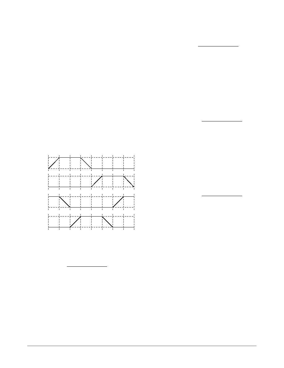
The disc (and pointer) respond to the vector sum of the
voltages applied to the coils. Ideally, this relationship
follows a sine/cosine equation. Since this is a transcendental
and non≠linear function, devices of this type use an
approximation for this relationship. The SACD uses a
tangential algorithm as shown in Figure 2. Only one output
varies in any 45 degree range.
SIN+
Output
Max(128)
SIN≠
Output
COS+
Output
COS≠
Output
Max(128)
Max(128)
Max(128)
Min(0)
Min(0)
Min(0)
Min(0)
0
∞
45
∞
90
∞
135
∞
180
∞
225
∞
270
∞
315
∞
360
∞
000
001
010
011
100
101
110
111
000
MUX bits (D9≠D7)
Degrees of Rotation
Figure 2. SIN, COS Outputs
Quadrant I
q +
Tan≠1
VSIN
) *
VSIN
*
VCOS
) *
VCOS
*
For
q +
0.176
∞
to 44.824
∞
:
VSIN
+
Tan
q
0.748
VBB
VCOS
+
0.748
VBB
For
q +
45.176
∞
to 89.824
∞
:
VSIN
+
0.748
VBB
VCOS
+
Tan(90
∞ * q
)
0.748
VBB
Quadrant II
q +
180
∞
≠Tan≠1
VSIN
) *
VSIN
*
VCOS
) *
VCOS
*
For
q +
90.176
∞
to 134.824
∞
:
VSIN
+
0.748
VBB
VCOS
+ *
Tan (
q *
90
∞
)
0.748
VBB
For
q +
135.176
∞
to 179.824
∞
:
VSIN
+
Tan(180
∞ * q
)
0.748
VBB
VCOS
+ *
0.748
VBB
Quadrant III
q +
180
∞ )
Tan≠1
VSIN
) *
VSIN
*
VCOS
) *
VCOS
*
For
q +
180.176
∞
to 224.824
∞
:
VSIN
+ *
Tan (
q *
180
∞
)
0.748
VBB
VCOS
+ *
0.748
VBB
For
q +
225.176
∞
to 269.824
∞
:
VSIN
+ *
0.748
VBB
VCOS
+ *
Tan (270
∞ * q
)
0.748
VBB
Quadrant IV
q +
360
∞ *
Tan≠1
VSIN
) *
VSIN
*
VCOS
) *
VCOS
*
For
q +
270.176
∞
to 314.824
∞
:
VSIN
+ *
0.748
VBB
VCOS
+
Tan(
q *
270
∞
)
0.748
VBB
For
q +
315.176
∞ *
359.824
∞
:
VSIN
+ *
Tan (360
∞ * q
)
0.748
VBB
VCOS
+
0.748
VBB

CS4192
http://onsemi.com
6
II
I
III
IV
270
∞
V
SIN≠
V
SIN+
90
∞
V
COS≠
V
COS+
180
∞
360/0
∞
0.748 V
BB
0.748 V
BB
0.748 V
BB
0.748 V
BB
Figure 3. Gauge Response
To drive the gauge's pointer to a particular angle, the
microcontroller sends a 10≠bit digital word into the serial
port. These 10 bits are divided as shown in Figure 4.
Gauge
(360
∞
)
MSB
LSB
D9
D8
D7
D6
D5
D4
D3
D2
D1
D0
D9≠D7 select
which octant
Divides a 45
∞
octant into 128 equal parts to
achieve a 0.35
∞
resolution Code 0≠127
10
Figure 4. Definition of Serial Word
However, from a software programmers viewpoint, a
360
∞
circle is divided into 1024 equal parts of 0.35
∞
each.
Table 1 shows the data associated with the 45
∞
divisions of
the 360
∞
driver.
Table1. Nominal Output (V
BB
= 14 V)
Input Code
(Decimal)
Ideal
Degrees
Nominal
Degrees
V
SIN
(V)
V
COS
(V)
0
0
0.176
0.032
10.476
128
45
45.176
10.476
10.412
256
90
90.176
10.476
≠0.032
384
135
135.176
10.412
≠10.476
512
180
180.176
≠0.032
≠10.476
640
225
225.176
≠10.476
≠10.412
768
270
270.176
≠10.476
0.032
896
315
315.176
≠10.476
10.476
1023
359.65
359.826
≠0.032
10.476
The 10 bits are shifted into the device's shift register MSB
first using an SPI compatible scheme. This method is shown
in Figure 5. The CS must be high and remain high for SCLK
to be enabled. Data on SI is shifted in on the rising edge of
the synchronous clock signal. Data in the shift register
changes at SO on the falling edge of SCLK. This
arrangement allows the cascading of devices. SO is always
enabled. Data shifts through without affecting the outputs
until CS is brought low. At this time the internal DAC is
updated and the outputs change accordingly.
CS
SI
SCLK
SO
SI
(Setup)
SI
(Hold)
SI
(tpd)
SO
(Rise, Fall)
10% ≠ 90%
CS
Hold
CS
Setup
Figure 5. Serial Data Timing Diagram
Figure 6 shows the power≠up sequence for the CS4192.
Note the IC requires a pulse on the Chip Select (CS) pin to
clear the Status Fault (ST) after power up. OE must be high
before the falling edge of CS to enable the output buffers.
V
CC
CS
SI
OE
ST
10
Bits
10
Bits
OUTPUTS
ENABLED
Registers
set to zero
Registers
set to zero
OUTPUTS
ENABLED
Figure 6. Power Up Sequence
CS4192
http://onsemi.com
7
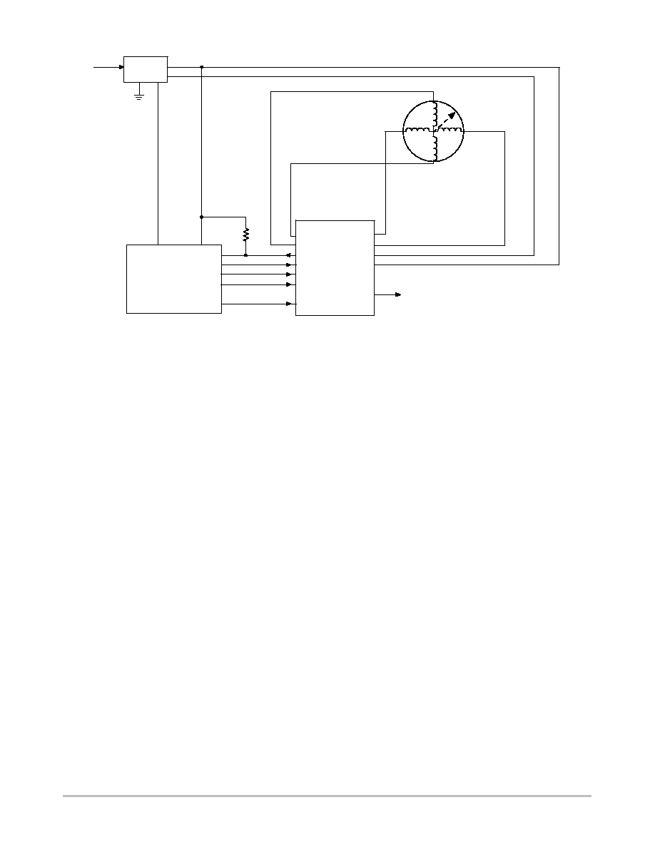
V
BATT
V
REG
CS8156
12 V
5.0 V
ENABLE
360
∞
Gauge
10 k
Microcontroller
SIN≠
SIN+
ST
CS
SI
SCLK
OE
COS+
COS≠
V
BB
V
CC
SO
Next Driver
Figure 7. Application Diagram
CS4192
CS4192
http://onsemi.com
8
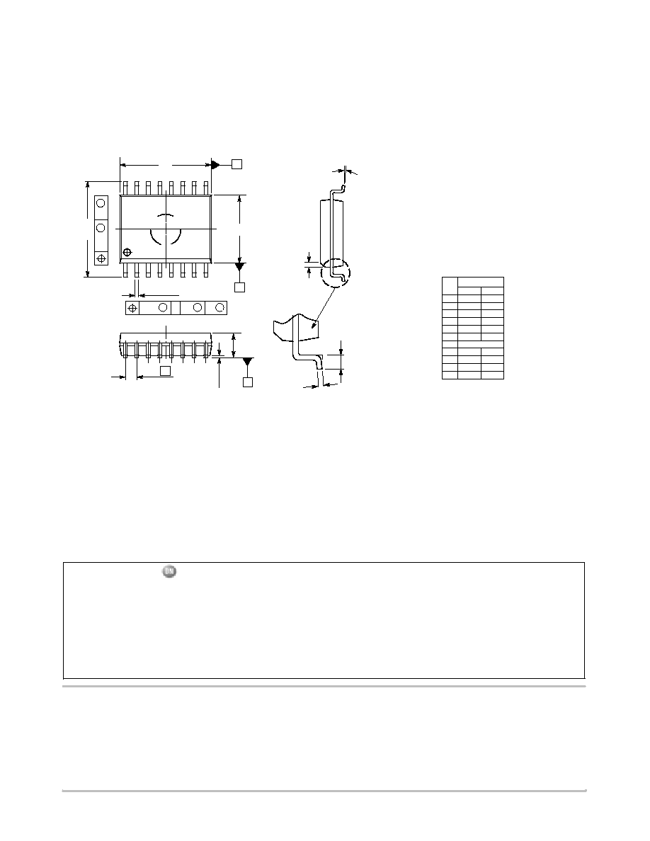
PACKAGE DIMENSIONS
SO≠16L
DWF SUFFIX
CASE 751G≠03
ISSUE B
D
14X
B
16X
SEATING
PLANE
S
A
M
0.25
B
S
T
16
9
8
1
h
X 45
_
M
B
M
0.25
H
8X
E
B
A
e
T
A1
A
L
C
q
NOTES:
1. DIMENSIONS ARE IN MILLIMETERS.
2. INTERPRET DIMENSIONS AND TOLERANCES
PER ASME Y14.5M, 1994.
3. DIMENSIONS D AND E DO NOT INLCUDE MOLD
PROTRUSION.
4. MAXIMUM MOLD PROTRUSION 0.15 PER SIDE.
5. DIMENSION B DOES NOT INCLUDE DAMBAR
PROTRUSION. ALLOWABLE DAMBAR
PROTRUSION SHALL BE 0.13 TOTAL IN EXCESS
OF THE B DIMENSION AT MAXIMUM MATERIAL
CONDITION.
DIM
MIN
MAX
MILLIMETERS
A
2.35
2.65
A1
0.10
0.25
B
0.35
0.49
C
0.23
0.32
D
10.15
10.45
E
7.40
7.60
e
1.27 BSC
H
10.05
10.55
h
0.25
0.75
L
0.50
0.90
q
0
7
_
_
ON Semiconductor and are trademarks of Semiconductor Components Industries, LLC (SCILLC). SCILLC reserves the right to make changes
without further notice to any products herein. SCILLC makes no warranty, representation or guarantee regarding the suitability of its products for any particular
purpose, nor does SCILLC assume any liability arising out of the application or use of any product or circuit, and specifically disclaims any and all liability,
including without limitation special, consequential or incidental damages. "Typical" parameters which may be provided in SCILLC data sheets and/or
specifications can and do vary in different applications and actual performance may vary over time. All operating parameters, including "Typicals" must be
validated for each customer application by customer's technical experts. SCILLC does not convey any license under its patent rights nor the rights of others.
SCILLC products are not designed, intended, or authorized for use as components in systems intended for surgical implant into the body, or other applications
intended to support or sustain life, or for any other application in which the failure of the SCILLC product could create a situation where personal injury or
death may occur. Should Buyer purchase or use SCILLC products for any such unintended or unauthorized application, Buyer shall indemnify and hold
SCILLC and its officers, employees, subsidiaries, affiliates, and distributors harmless against all claims, costs, damages, and expenses, and reasonable
attorney fees arising out of, directly or indirectly, any claim of personal injury or death associated with such unintended or unauthorized use, even if such claim
alleges that SCILLC was negligent regarding the design or manufacture of the part. SCILLC is an Equal Opportunity/Affirmative Action Employer.
PUBLICATION ORDERING INFORMATION
JAPAN: ON Semiconductor, Japan Customer Focus Center
4≠32≠1 Nishi≠Gotanda, Shinagawa≠ku, Tokyo, Japan 141≠0031
Phone: 81≠3≠5740≠2700
Email: r14525@onsemi.com
ON Semiconductor Website: http://onsemi.com
For additional information, please contact your local
Sales Representative.
CS4192/D
Literature Fulfillment:
Literature Distribution Center for ON Semiconductor
P.O. Box 5163, Denver, Colorado 80217 USA
Phone: 303≠675≠2175 or 800≠344≠3860 Toll Free USA/Canada
Fax: 303≠675≠2176 or 800≠344≠3867 Toll Free USA/Canada
Email: ONlit@hibbertco.com
N. American Technical Support: 800≠282≠9855 Toll Free USA/Canada