©
Semiconductor Components Industries, LLC, 2004
January, 2004 - Rev. 5
1
Publication Order Number:
CS5231-3/D
CS5231-3
500 mA, 3.3 V Linear
Regulator with Auxiliary
Control
The CS5231-3 combines a three-terminal linear regulator with
circuitry controlling an external PFET transistor thus managing two
input supplies. The part provides a 3.3 V regulated output either from
the main 5.0 V supply or a 3.3 V auxiliary that switches on when the
5.0 V supply is not present. This delivers constant, uninterrupted
power to the load. The CS5231-3 meets Intel's "Instantly Available"
power requirements which follows from the "Advanced Configuration
and Power Interface" (ACPI) standards developed by Intel, Microsoft
and Toshiba.
The CS5231-3 linear regulator provides a fixed 3.3 V output at
500 mA with an overall accuracy of
±
2.0%. The internal NPN-PNP
composite pass transistor provides a low dropout voltage and requires
less supply current than a straight PNP design. Full protection with
both current limit and thermal shutdown is provided.
Designed for low reverse current, the IC prevents excessive current
from flowing from V
OUT
to either V
IN
or ground when the regulator
input voltage is lower than the output voltage.
The CS5231-3 can be used to provide power to an ASIC on a PCI
Network Interface Card (NIC). When the system enters a Sleep State
and the 5.0 V input drops below 4.4 V, the AuxDrv control signal on the
CS5231-3 is activated turning on the external PFET. This switches the
supply source from the 5.0 V input to the 3.3 V input through the PFET,
guaranteeing a constant 3.3 V output to the ASIC that is "glitch free."
The CS5231-3 is available in two package types: the D
2
PAK-5
(TO263) package and the SOIC-8 4-Lead-fused (DF) package. Other
applications include desktop computers, power supplies with multiple
input sources and PCMCIA/PCI interface cards.
Features
∑
Linear Regulator
-
3.3 V
±
2.0% Output Voltage
-
3.0 mA Quiescent Current @ 500 mA
-
Fast Transient Response
-
Current Limit Protection
-
Thermal Shutdown with Hysteresis
-
450
mA Reverse Output Current
∑
System Power Management
-
Auxiliary Supply Control
-
"Glitch Free" Transition Between Two Supplies
∑
Internally Fused Leads in SOIC-8 Package
PIN CONNECTIONS AND
MARKING DIAGRAMS
A
= Assembly Location
WL, L
= Wafer Lot
YY, Y
= Year
WW, W = Work Week
Device
Package
Shipping
ORDERING INFORMATION
CS5231-3GDP5
D
2
PAK-5
50 Units/Rail
CS5231-3GDPR5
D
2
PAK-5
750 Tape & Reel
CS5231-3GDF8
SOIC-8
95 Units/Rail
CS5231-3GDFR8
SOIC-8
2500 Tape & Reel
SOIC-8
DF SUFFIX
CASE 751
Pin 1. No Connect
2. V
IN
3. GND
4. V
OUT
5. AuxDrv
Tab = GND
D
2
PAK-5
DP SUFFIX
CASE 936AC
CS5231-3
AWLYWW
1
1
5
V
OUT
V
IN
1
5231-
AL
YW3
8
GND
GND
GND
GND
AuxDrv
NC
1
8
SOIC-8
D
2
PAK-5
http://onsemi.com
For information on tape and reel specifications,
including part orientation and tape sizes, please
refer to our Tape and Reel Packaging Specifications
Brochure, BRD8011/D.
CS5231-3
http://onsemi.com
2
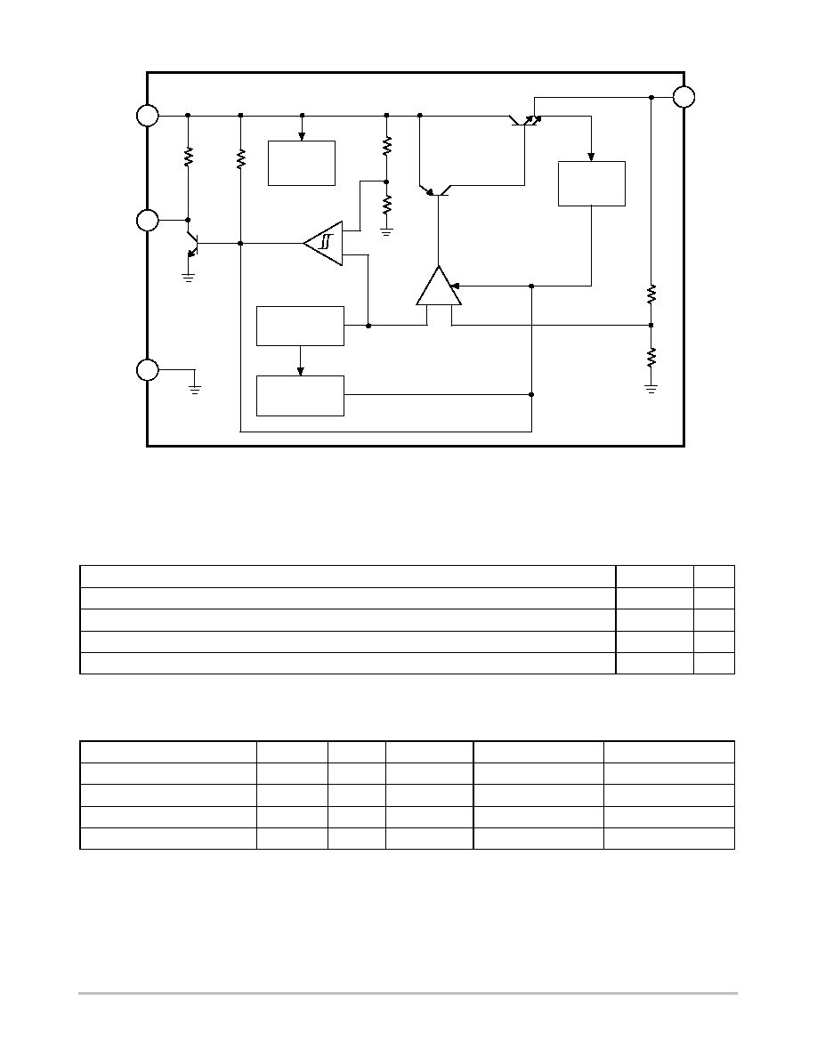
Thermal
Shutdown
V
IN
GND
10 k
W
Error
Amp
Current
Limit
Shutdown
AuxDrv
Internal
Bias
V
OUT
Figure 1. Block Diagram
-
+
-
+
Bandgap
Reference
50 k
W
V
IN
UV
Comparator
V
REF
ABSOLUTE MAXIMUM RATINGS*
Rating
Value
Unit
Maximum Operating Junction Temperature
150
∞
C
Storage Temperature Range
-65 to +150
∞
C
Lead Temperature Soldering:
Reflow: (SMD styles only) (Note 1)
230 peak
∞
C
ESD Damage Threshold (Human Body Model)
2.0
kV
1. 60 second maximum above 183
∞
C.
*The maximum package power dissipation must be observed.
ABSOLUTE MAXIMUM RATINGS
Pin Name
Pin Symbol
V
MAX
V
MIN
I
SOURCE
I
SINK
IC Power Input
V
IN
14 V
-0.3 V
100 mA
Internally Limited
Output Voltage
V
OUT
6.0 V
-0.3 V
Internally Limited
100 mA
Auxiliary Drive Output
AuxDrv
14 V
-0.3 V
10 mA
50 mA
IC Ground
GND
N/A
N/A
N/A
N/A
CS5231-3
http://onsemi.com
3
ELECTRICAL CHARACTERISTICS
(0
∞
C < T
A
< 70
∞
C; 0
∞
C < T
J
< 125
∞
C; 4.75
V
V
CC
< 6.0 V; C
OUT
10
m
F with
ESR < 1.0
W
, I
OUT
= 10 mA; unless otherwise specified.)
Characteristic
Test Conditions
Min
Typ
Max
Unit
Linear Regulator
Output Voltage
10 mA < I
OUT
< 500 mA.
3.234
(- 2%)
3.3
3.366
(+ 2%)
V
Line Regulation
I
OUT
= 10mA; V
IN
= 4.75 V to 6.0 V
-
1.0
5.0
mV
Load Regulation
V
IN
= 5.0 V; I
OUT
= 10 mA to 500 mA
-
5.0
15
mV
Ground Current
I
OUT
= 10 mA
I
OUT
= 500 mA
-
-
2.0
3.0
3.0
6.0
mA
mA
Reverse Current
V
IN
= 0 V, V
OUT
= 3.3 V
-
0.45
1.0
mA
Current Limit
0 V < V
OUT
< 3.2 V
0.55
0.85
1.2
A
Thermal Shutdown
Note 2
150
180
210
∞
C
Thermal Shutdown Hysteresis
Note 2
-
25
-
∞
C
Auxiliary Drive
Upper V
IN
Threshold
Increase V
IN
until regulator turns on and
AuxDrv drives high
4.35
4.5
4.65
V
Lower V
IN
Threshold
Decrease V
IN
until regulator turns off and
AuxDrv drives low
4.25
4.4
4.55
V
V
IN
Threshold Hysteresis
-
75
100
125
mV
Output Low Voltage
I
AuxDrv
= 100
m
A, 1.0 V < V
IN
< 4.5 V
-
0.1
0.4
V
Output Low Peak Voltage
Increase V
IN
from 0V to 1.0 V.
Record peak AuxDrv output voltage
-
0.65
0.9
V
AuxDrv Current Limit
V
AuxDrv
= 1.0 V; V
IN
= 4.0 V
0.5
6.0
25
mA
Response Time
Step V
IN
from 5.0 V to 4.0 V, measure time for
V
AuxDrv
to drive low. Note 2
-
1.0
10
m
s
Pull-Up/Down Resistance
V
IN
= 0 V and V
IN
> 4.7 V.
5.0
10
25
k
W
2. Guaranteed by design, not 100% production tested. Thermal shutdown is 100% functionally tested at wafer probe.
PACKAGE PIN DESCRIPTION
Package Lead #
D
2
PAK-5
SOIC-8
Lead Symbol
Function
1
1
NC
No connection.
2
4
V
IN
Input voltage.
3, Tab
2, 3, 6, 7
GND
Ground and IC substrate connection.
4
5
V
OUT
Regulated output voltage.
5
8
AuxDrv
Output used to control an auxiliary supply voltage. This lead is driven
low if V
IN
is less than 4.5 V, and is otherwise pulled up to V
IN
through
an internal 10 k
W
resistor.
CS5231-3
http://onsemi.com
4
TYPICAL PERFORMANCE CHARACTERISTICS
Figure 2. Output Voltage vs. Junction Temperature
Junction Temperature (
∞
C)
3.302
3.300
3.298
120
0
3.296
Output V
oltage (V)
100
80
60
40
20
I
OUT
(A)
0
Load Regulation (mV)
0.2
1.2
1.0
0.8
0.6
0.4
0.2
0
0.4
Figure 3. Line Regulation vs. I
OUT
Over
Temperature
I
OUT
(A)
0.8
0.0
Load Regulation (mV)
0.2
0.6
0.4
0.2
0.0
0.4
Figure 4. Load Regulation vs. I
OUT
Over
Temperature
125
∞
C
Junction Temperature (
∞
C)
380
0
Reverse Current (
m
A)
20
370
360
40
60
80
100
120
Figure 5. Reverse Current vs. Junction
Temperature
Figure 6. V
OUT
vs. I
OUT
Over Junction
Temperature
Figure 7. V
IN
Thresholds vs. Junction
Temperature
1.0
1.2
I
OUT
(A)
0.0
V
OUT
(V)
0.2
3
2
1
0
0.4
0.6
0.8
1.0
Junction Temperature (
∞
C)
4.52
4.50
4.48
4.46
120
0
4.38
V
IN
Threshold V
oltage (V)
100
80
60
40
20
4.44
4.42
4.40
V
IN
Turn-On
Threshold
V
IN
Turn-Off
Threshold
27
∞
C
0
∞
C
125
∞
C
27
∞
C
0
∞
C
I
OUT
= 10 mA
I
OUT
= 500 mA
27
∞
C
125
∞
C
0
∞
C
140
390
CS5231-3
http://onsemi.com
5
Figure 8. Ground Current vs. Load Current
Capacitance ESR (
W
)
1000
6.0
0
10
Capacitance (
m
F)
5.0
4.0
3.0
2.0
1.0
100
Figure 9. Region of Stable Operation
Temperature (
∞
C)
4.4
0
4.0
Current Limit (mA)
40
20
4.2
60
Figure 10. AuxDrv Current Limit vs. Junction
Temperature
Load Current (A)
0.0
Ground Current (mA)
0.2
2.2
2.0
1.8
1.6
0.4
T
J
= 0
∞
C
I
GND
@ 0
∞
C
2.4
2.6
4.6
4.8
5.0
80
100
120
140
Time, 5.0
m
s per division
3.2
10
V
OUT
500
Figure 11. Transient Response
3.3
3.4
I
OUT
(m
A
)
T
J
= 27
∞
C
I
GND
@ 27
∞
C
T
J
= 125
∞
C
I
GND
@ 125
∞
C
C
IN
= 33
m
F
C
OUT
= 33
m
F
V
IN
= 5.00 V
Stable Region
T
J
= 25
∞
C
7.0
Figure 12. Application Circuit
5.0 V PCI
C1
33
m
F
V
IN
GND
AuxDrv
V
OUT
3.3 V V
AUX
C1
33
m
F
C3
33
m
F
M1
ASIC
V
DD
* indicates PFET body diode
CS5231-3
CS5231-3
http://onsemi.com
6
APPLICATION INFORMATION
THEORY OF OPERATION
The CS5231-3 is a fixed 3.3 V linear regulator that
contains an auxiliary drive control feature. When V
IN
is
greater than the typical 4.5 V threshold, the IC functions as
a linear regulator. It provides up to 500 mA of current to a
load through a composite PNP-NPN pass transistor. An
output capacitor greater than 10
mF with equivalent series
resistance less than 1.0
W is required for compensation.
More information is provided in the Stability Considerations
section.
The CS5231-3 provides an auxiliary drive feature that
allows a load to remain powered even if the V
IN
supply for
the IC is absent. An external p-channel FET is the only
additional component required to implement this function if
an auxiliary power supply is available. The PFET gate is
connected to the AuxDrv lead. The PFET drain is connected
to the auxiliary power supply, and the PFET source is
connected to the load. The polarity of this connection is very
important, since the PFET body diode will be connected
between the load and the auxiliary supply. If the PFET is
connected with its drain to the load and its source to the
supply, the body diode will be forward-biased if the
auxiliary supply is turned off. This will result in the linear
regulator providing current to everything on the auxiliary
supply rail.
The AuxDrv lead is internally connected to a 10 k
W
resistor and to a saturating NPN transistor that acts as a
switch. If the V
IN
supply is off, the AuxDrv output will
connect the PFET gate to ground through the 10 k
W resistor,
and the PFET will conduct current to the load.
As the V
IN
supply begins to rise, the AuxDrv lead will also
rise until it reaches a typical voltage of about 650 mV. The
NPN transistor connected to the AuxDrv lead will saturate
at this point, and the gate of the PFET will be pulled down
to a typical voltage of about 100 mV. The PFET will
continue to conduct current to the load.
The V
IN
supply voltage will continue to rise, but the linear
regulator output is disabled until V
IN
reaches a typical
threshold of 4.5 V. During this time, the load continues to be
powered by the auxiliary driver. Once the 4.5 V V
IN
threshold is reached, the saturating NPN connected to the
AuxDrv lead turns off. The on-chip 10 k
W pull-up resistor
will pull the PFET gate up to V
IN
, thus turning the PFET off.
The linear regulator turns on at the same time. An external
compensation capacitor is required for the linear regulator
to be stable, and this capacitance also serves as a charge
reservoir to minimize any "glitching" that might result
during the supply changeover. Hysteresis is present in the
AuxDrv circuitry, requiring V
IN
to drop by 100 mV (typical)
after the linear regulator is providing power to the load
before the AuxDrv circuitry can be re-enabled.
Figure 13. Initial Power-Up, V
AUX
Not
Present R
OUT
= 8.8
W
I
OUT
= STARTUP 375 mA
V
IN
V
OUT
V
AUXDRV
Figure 14. Power-Up, V
AUX
= 3.3 V. Note the
"Oscillatory Performance" as the Linear Regulator
Changes the V
OUT
Node. I
OUT
y
R
DS(ON)
9
130 mV
I
OUT
= 375 mA V
AUX
= 3.30 V
V
IN
V
OUT
V
AUXDRV
Figure 15. Power-Down, V
AUX
= 3.3 V. Again,
Note
D
V = I R
DS(ON)
9
130 mV
I
OUT
= 375 mA V
AUX
= 3.30
V
IN
V
OUT
V
AUXDRV
CS5231-3
http://onsemi.com
7
Figure 16. Power-Up, V
AUX
= 3.135 V. The
"Oscillatory Performance" Mode Lasts Longer
Because the Difference Between V
AUX
and 3.3 is
Greater
I
OUT
= 375 mA V
AUX
= 3.135 V
V
IN
V
OUT
V
AUXDRV
Figure 17. Power-Down, V
AUX
= 3.135 V. The
Difference in Voltage is Now I
OUT
y
R
DS(ON)
Plus
the Difference in Supply Voltages (3.3 - V
AUX
)
I
OUT
= 375 mA V
AUX
= 3.135
V
IN
V
OUT
V
AUXDRV
Figure 18. Power-Up, V
AUX
= 3.465 V. I
OUT
y
R
DS(ON)
is Compensated By Higher Value of V
AUX
I
OUT
= 375 mA V
AUX
= 3.465
V
IN
V
OUT
V
AUXDRV
Figure 19. Power-Down, V
AUX
= 3.465 V
I
OUT
= 375 mA V
AUX
= 3.465
V
IN
V
OUT
V
AUXDRV
STABILITY CONSIDERATIONS
The output capacitor helps determine three main
characteristics of a linear regulator: startup, transient
response and stability.
Startup is affected because the output capacitor must be
charged. At initial startup, the V
IN
supply may not be
present, and the output capacitor will be charged through the
PFET. The PFET will initially provide current to the load
through its body diode. The diode will act as a voltage
follower until sufficient voltage is present to turn the FET
on. Since most commercial power supplies have a fairly low
ramp rate, charging through the body diode should
effectively limit in-rush current to the capacitor.
During normal operation, transient load current
requirements will be satisfied from the charge stored in the
output capacitor until either the linear regulator or the
auxiliary supply can respond. Larger values of capacitance
will improve transient response, but will also cost more. A
linear regulator will respond within microseconds, where an
external power supply may take milliseconds to react. The
output capacitance will provide the difference in current
until this occurs. The result will be an instantaneous voltage
change at the output. This change is the product of the
current change and the capacitor ESR:
D
VOUT
+ D
ILOAD
ESR
This limitation directly affects load regulation. Capacitor
ESR must be minimized if output voltage must be
maintained within tight tolerances. In such a case, it is often
advisable to use a parallel network of different types of
capacitors. For example, electrolytic capacitors provide
high charge storage capacity in a small size, while tantalum
capacitors have low ESR. The parallel combination will
result in a high capacity, low ESR network. It is also
important to physically locate the capacitance network close
to the load, and to connect the network to the load with wide
PC board traces to minimize the metal resistance.

CS5231-3
http://onsemi.com
8
The CS5231-3 has been carefully designed to be stable
for output capacitances greater than 10
mF with equivalent
series resistance less than 1.0
W. While careful board layout
is important, the user should have a stable system if these
constraints are met. A graph showing the region of stability
for the CS5231-3 is included in the "Typical Performance
Characteristics" section of this datasheet.
INPUT CAPACITORS AND THE V
IN
THRESHOLDS
A capacitor placed on the V
IN
pin will help to improve
transient response. During a load transient, the input
capacitor serves as a charge "reservoir," providing the
needed extra current until the external power supply can
respond. One of the consequences of providing this current
is an instantaneous voltage drop at V
IN
due to capacitor
ESR. The magnitude of the voltage change is again the
product of the current change and the capacitor ESR.
It is very important to consider the maximum current step
that can exist in the system. If the change in current is large
enough, it is possible that the instantaneous voltage drop on
V
IN
will exceed the V
IN
threshold hysteresis, and the IC will
enter a mode of operation resembling an oscillation. As the
part turns on, the output current I
OUT
will increase, reaching
current limit during initial charging. Increasing I
OUT
results
in a drop at V
IN
such that the shutdown threshold is reached.
The part will turn off, and the load current will decrease. As
I
OUT
decreases, V
IN
will rise and the part will turn on,
starting the cycle all over again. This oscillatory operation
is most likely at initial start-up when the output capacitance
is not charged, and in cases where the ramp-up of the V
IN
supply is slow. It may also occur during the power transition
when the regulator turns on and the PFET turns off. A 15
ms
delay exists between turn-on of the regulator and the
AuxDrv pin pulling the gate of the PFET high. This delay
prevents "chatter" during the power transitions. During this
interval, the linear regulator will attempt to regulate the
output voltage as 3.3 V. If the output voltage is significantly
below 3.3 V, the IC will go into current limit while trying to
raise V
OUT
. It is a short-lived phenomenon and is mentioned
here to alert the user that the condition can exist. It is
typically not a problem in applications. Careful choice of the
PFET switch with respect to R
DS(ON)
will minimize the
voltage drop which the output must charge through to return
to a regulated state. More information is provided in the
section on choosing the PFET switch.
If required, using a few capacitors in parallel to increase
the bulk charge storage and reduce the ESR should give
better performance than using a single input capacitor.
Short, straight connections between the power supply and
V
IN
lead along with careful layout of the PC board ground
plane will reduce parasitic inductance effects. Wide V
IN
and
V
OUT
traces will reduce resistive voltage drops.
CHOOSING THE PFET SWITCH
The choice of the external PFET switch is based on two
main considerations. First, the PFET should have a very low
turn-on threshold. Choosing a switch transistor with
V
GS(ON)
1.0 V will ensure the PFET will be fully enhanced
with only 3.3 V of gate drive voltage. Second, the switch
transistor should be chosen to have a low R
DS(ON)
to
minimize the voltage drop due to current flow in the switch.
The formula for calculating the maximum allowable
on-resistance is
RDS(ON)MAX
+
VAUX(MIN)
*
VOUT(MIN)
1.5
IOUT(MAX)
where V
AUX(MIN)
is the minimum value of the auxiliary
supply voltage, V
OUT(MIN)
is the minimum allowable
output voltage, I
OUT(MAX)
is the maximum output current
and 1.5 is a "fudge factor" to account for increases in
R
DS(ON)
due to temperature.
OUTPUT VOLTAGE SENSING
It is not possible to remotely sense the output voltage of
the CS5231-3 since the feedback path to the error amplifier
is not externally available. It is important to minimize
voltage drops due to metal resistance of high current PC
board traces. Such voltage drops can occur in both the
supply traces and the return traces.
The following board layout practices will help to
minimize output voltage errors:
∑
Always place the linear regulator as close to both load
and output capacitors as possible.
∑
Always use the widest possible traces to connect the
linear regulator to the capacitor network and to the
load.
∑
Connect the load to ground through the widest possible
traces.
∑
Connect the IC ground to the load ground trace at the
point where it connects to the load.
CURRENT LIMIT
The CS5231-3 has internal current limit protection.
Output current is limited to a typical value of 850 mA, even
under output short circuit conditions. If the load current
drain exceeds the current limit value, the output voltage will
be pulled down and will result in an out of regulation
condition. The IC does not contain circuitry to report this
fault.
THERMAL SHUTDOWN
The CS5231-3 has internal temperature monitoring
circuitry. The output is disabled if junction temperature of
the IC reaches 180
∞
C. Thermal hysteresis is typically 25
∞
C
and allows the IC to recover from a thermal fault without the
CS5231-3
http://onsemi.com
9
need for an external reset signal. The monitoring circuitry is
located near the composite PNP-NPN output transistor,
since this transistor is responsible for most of the on-chip
power dissipation. The combination of current limit and
thermal shutdown will protect the IC from nearly any fault
condition.
REVERSE CURRENT PROTECTION
During normal system operation, the auxiliary drive
circuitry will maintain voltage on the V
OUT
pin when V
IN
is absent. IC reliability and system efficiency are improved
by limiting the amount of reverse current that flows from
V
OUT
to ground and from V
OUT
to V
IN
. Current flows from
V
OUT
to ground through the feedback resistor divider that
sets up the output voltage This resistor can range in value
from 6.0 k
W to about 10 kW, and roughly 500 mA will flow
in the typical case. Current flow from V
OUT
to V
IN
will be
limited to leakage current after the IC shuts down. On-chip
RC time constants are such that the output transistor should
be turned off well before V
IN
drops below the V
OUT
voltage.
CALCULATING POWER DISSIPATION AND
HEATSINK REQUIREMENTS
Most linear regulators operate under conditions that result
in high on-chip power dissipation. This results in high
junction temperatures. Since the IC has a thermal shutdown
feature, ensuring the regulator will operate correctly under
normal conditions is an important design consideration.
Some heatsinking will usually be required.
Thermal characteristics of an IC depend on four
parameters: ambient temperature (T
A
in
∞
C), power
dissipation (P
D
in watts), thermal resistance from the die to
the ambient air (
q
JA
in
∞
C per watt) and junction temperature
(T
J
in
∞
C). The maximum junction temperature is calculated
from the formula below:
TJ(MAX)
+
TA(MAX)
)
(
q
JA
PD(MAX))
Maximum ambient temperature and power dissipation are
determined by the design, while
q
JA
is dependent on the
package manufacturer. The maximum junction temperature
for operation of the CS5231-3 within specification is
150
∞
C. The maximum power dissipation of a linear
regulator is given as
PD(MAX)
+
(VIN(MAX)
*
VOUT(MIN))
(ILOAD(MAX)
)
VIN(MAX))
IGND(MAX)
where I
GND(MAX)
is the IC bias current.
It is possible to change the effective value of
q
JA
by adding
a heatsink to the design. A heatsink serves in some manner
to raise the effective area of the package, thus improving the
flow of heat from the package into the surrounding air. Each
material in the path of heat flow has its own characteristic
thermal resistance, all measured in
∞
C per watt. The thermal
resistances are summed to determine the total thermal
resistance between the die junction and air. There are three
components of interest: junction-to-case thermal resistance
(
q
JC
), case-to-heatsink thermal resistance (
q
CS
) and
heatsink-to-air thermal resistance (
q
SA
). The resulting
equation for junction-to-air thermal resistance is
q
JA
+ q
JC
) q
CS
) q
SA
The value of
q
JC
both packages of the CS5231-3 are
provided in the Packaging Information section of this data
sheet. The value of
q
CS
can be considered zero, since heat is
conducted out of the D
2
PAK package by the IC leads and the
tab, and out of the SOIC-8 package by its IC leads that are
soldered directly to the PC board.
Modification of
q
SA
is the primary means of thermal
management. For surface mount components, this means
modifying the amount of trace metal that connects to the IC.
The thermal capacity of PC board traces is dependent on
how much copper area is used, whether or not the IC is in
direct contact with the metal, whether or not the metal
surface is coated with some type of sealant, and whether or
not there is airflow across the PC board. The chart provided
below shows heatsinking capability of a square, single sided
copper PC board trace. The area is given in square
millimeters, and it is assumed there is no airflow across the
PC board.
Figure 20. Thermal Resistance Capability of
Copper PC Board Metal Traces
PC Board Trace Area (mm
2
)
70
0
Thermal Resistance,
∞
CW
2000
50
60
40
30
20
10
0
4000
6000
TYPICAL D
2
PAK PC BOARD HEATSINK DESIGN
A typical design of the PC board surface area needed for
the D
2
PAK package is shown on page 11. Calculations were
made assuming V
IN(MAX)
= 5.25 V, V
OUT(MIN)
= 3.266 V,
I
OUT(MAX)
= 500 mA, I
GND(MAX)
= 5.0 mA and T
A
= 70
∞
C.
PD
+
(5.25 V
*
3.266 V)
0.5 A
)
(5.25 V)(0.005 A)
+
1018 mW
Maximum temperature rise
D
T
+
TJ(MAX)
*
TA
+
150
∞
C
*
70
∞
C
+
80
∞
C
q
JA(worst case)
+ D
T PD
+
80
∞
C 1.018 W
+
78.56
∞
C W
CS5231-3
http://onsemi.com
10
First, we determine the need for heatsinking. If we assume
the maximum
q
JA
= 50
∞
C/W for the D
2
PAK, the maximum
temperature rise is found to be
D
T
+
PD
q
JA
+
1.018 W
50
∞
C W
+
50.9
∞
C
This is less than the maximum specified operating
junction temperature of 125
∞
C, and no heatsinking is
required. Since the D
2
PAK has a large tab, mounting this
part to the PC board by soldering both tab and leads will
provide superior performance with no PC board area
penalty.
TYPICAL FUSED SOIC-8 DESIGN
We first determine the need for a heat sink for the SOIC-8
package at a load of 500 mA. Using the dissipation from the
D
2
PAK example of 1018 mW and the
q
JA
of the SOIC-8
package of 110
∞
C/W gives a temperature rise of 112
∞
C.
Adding this to an ambient temperature of 70
∞
C gives 182
∞
C
junction temperature. This is an excessive temperature rise
but it can be reduced by adding additional cooling in the
form of added surface area of copper on the PCB. Using the
relationship of maximum temperature rise of
D
TJA
+
TJ(MAX)
*
TA
+
150
∞
C
*
70
∞
C
+
80
∞
C
We calculate the thermal resistance allowed from junction
to air:
q
JA(worst case)
+ D
TJA PD
+
80
∞
C 1.018 W
+
79.6
∞
C W
The thermal resistance from the die to the leads (case) is
25
∞
C/W. Subtracting these two numbers gives the allowable
thermal resistance from case to ambient:
q
CA
+ q
JA
* q
JC
+
79.6
∞
C W
*
25
∞
C W
+
54.6
∞
C W
The thermal resistance of this copper area will be
54.6
∞
C/W. We now look at Figure 20 and find the PCB trace
area that will be less than 54.5
∞
C/W. Examination shows that
750 mm
2
of copper will provide cooling for this part. This
would be the SOIC-8 part with the center 4 ground leads
soldered to pads in the center of a copper area about 27 mm
◊
27 mm. A lower dissipation or the addition of air-flow
could result in a smaller required surface area.
DESCRIPTION
The CS5231-3 application circuit has been implemented
as shown in the following pages. The schematic, bill of
materials and printed circuit board artwork can be used to
build the circuit. The design is very simple and consists of
two capacitors, a p-channel FET and the CS5231-3. Five
turret pins are provided for connection of supplies, meters,
oscilloscope probes and loads. The CS5231-3 power supply
management solution is implemented in an area less than 1.5
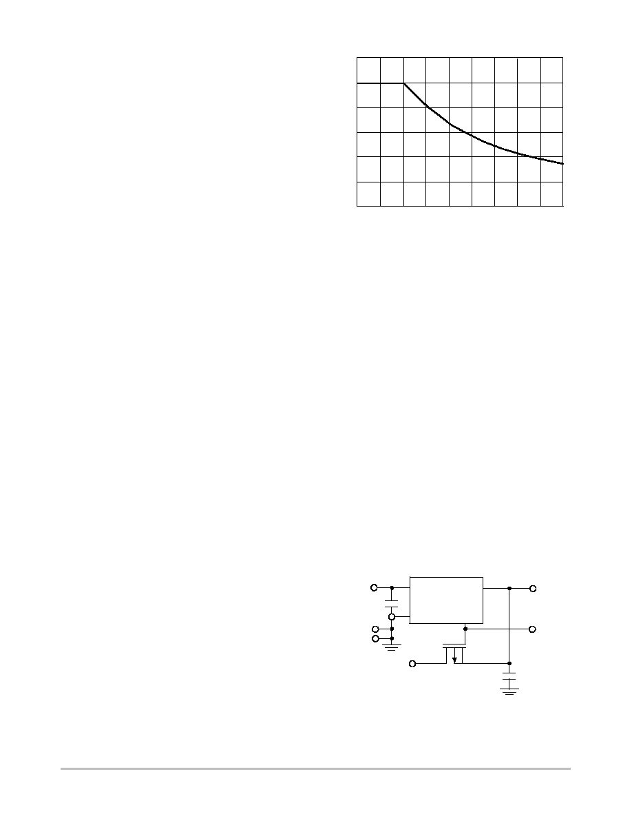
square inches. Due to the simplicity of the design, output
current must be derated if the CS5231-3 is operated at V
IN
voltages greater than 7.0 V. Figure 21 provides the derating
curve on a maximum power dissipation if heatsink is added.
Operating at higher power dissipation without CS5231-3
heatsink may result in a thermal shutdown condition.
Figure 21. Demo Board Output Current
Derating vs. V
IN
V
IN
(Volts)
5
I
OUT
(mA)
6
500
600
400
300
200
100
0
7
8
9
10
11
12
13
14
The V
IN
Connection
The V
IN
connection is denoted as such on the PC board.
The maximum input voltage to the IC is 14 V before damage
to the IC is possible. However, the specification range for the
IC is 4.75 V < V
IN
< 6.0 V.
The GND Connection
The GND connection ties the IC power return to two turret
pins. The extra turret pin provides for connection of multiple
instrument grounds to the demonstration board.
The AuxDrv Connection
The AuxDrv lead of the CS5231-3 is connected to the gate
of the external PFET. This connection is also brought to a
turret pin to allow easy connection of an oscilloscope probe
for viewing the AuxDrv waveforms.
The V
AUX
Connection
The V
AUX
turret pin provides a connection point between
an external 3.3 V supply and the PFET drain.
The V
OUT
Connection
The V
OUT
connection is tied to the V
OUT
lead of the
CS5231-3 and the PFET source. This point provides a
convenient point at which some type of lead may be applied.
Figure 22. Application Circuit Schematic
TP5
TP6
AuxDrv
TP1
TP2
TP3
TP4
V
AUX
+3.3 V
C2
Q1
U1
V
OUT
V
IN
GND
AuxDrv
CS5231-3
V
IN
GND
C1
CS5231-3
http://onsemi.com
11
PC Board Layout Artwork
The PC Board is a single layer copper design. The layout
artwork is reproduced at actual size below.
Figure 23. Top Copper Layer
Figure 24. Top Silk Screen Layer
2"
1.8"
2"
1.8"
V
IN
5.0 V
GND
GND
V
OUT
3.3 V
AUX 3.3 V
AUX.DRV
Test Description
The startup and supply transition waveforms shown in
Figures 13 through 19 were obtained using the application
circuit board with a resistive load of 8.8
W. This provides a
DC load of 375 mA when the regulated output voltage is 3.3
V. A standard 2.0 A bench supply was used to provide power
to the application circuit. The transient response waveforms
shown in the Typical Performance Characteristics section
were obtained by switching a 6.3
W resistor across the
output.
Temperature Performance
The graph below shows thermal performance for the
CS5231-3 across the normal operating output current range.
Figure 25. Package Temperature vs. Load
Current (V
IN
= 5.0 V, T
A
= 23
5
C)
Load Current (mA)
55
0
Package T
emperature (C)
50
45
50
40
35
30
25
20
100 150 200 250 300 350 400 450 500
PFET R
DS(ON)
Performance
The graph provided below show typical R
DS(ON)
performance for the PFET. The data is provided as V
DS
vs
I
OUT
for different values of V
AUX
.
Figure 26. PFET V
DS
vs. I
OUT
I
OUT
(mA)
140
0
V
DS
(mV)
100
100
120
80
60
40
20
0
200
300
400
500
160
V
AUX
= 3.135 V
V
AUX
= 3.300 V
V
AUX
= 3.465 V
APPLICATIONS CIRCUIT BILL OF MATERIALS
Ref des
¡¡¡¡¡¡¡¡¡
¡¡¡¡¡¡¡¡¡
Description
¡¡¡¡¡¡¡
¡¡¡¡¡¡¡
Part Number
Manufacturer
¡¡¡¡¡¡¡¡
¡¡¡¡¡¡¡¡
Contact Information
C1, C2
¡¡¡¡¡¡¡¡¡
¡
¡¡¡¡¡¡¡
¡
¡¡¡¡¡¡¡¡¡
33
m
F, 16 V tantalum capacitors
¡¡¡¡¡¡¡
¡
¡¡¡¡¡
¡
¡¡¡¡¡¡¡
TAJD336K016
AVX Corp
¡¡¡¡¡¡¡¡
¡
¡¡¡¡¡¡
¡
¡¡¡¡¡¡¡¡
www.avxcorp.com
1-843-448-9411
Q1
¡¡¡¡¡¡¡¡¡
¡¡¡¡¡¡¡¡¡
p-channel FET transistor
¡¡¡¡¡¡¡
¡¡¡¡¡¡¡
MGSF1P02ELT1
ON Semiconductor
¡¡¡¡¡¡¡¡
¡¡¡¡¡¡¡¡
http://onsemi.com
U1
¡¡¡¡¡¡¡¡¡
¡¡¡¡¡¡¡¡¡
Linear regulator with auxiliary
¡¡¡¡¡¡¡
¡¡¡¡¡¡¡
CS5231-3DPS
ON Semiconductor
¡¡¡¡¡¡¡¡
¡¡¡¡¡¡¡¡
http://onsemi.com
T1-T6
¡¡¡¡¡¡¡¡¡
¡
¡¡¡¡¡¡¡
¡
¡¡¡¡¡¡¡¡¡
Turret pins
¡¡¡¡¡¡¡
¡
¡¡¡¡¡
¡
¡¡¡¡¡¡¡
40F6023
Newark Electronics
¡¡¡¡¡¡¡¡
¡
¡¡¡¡¡¡
¡
¡¡¡¡¡¡¡¡
www.newark.com
1-800-463-9275

CS5231-3
http://onsemi.com
12
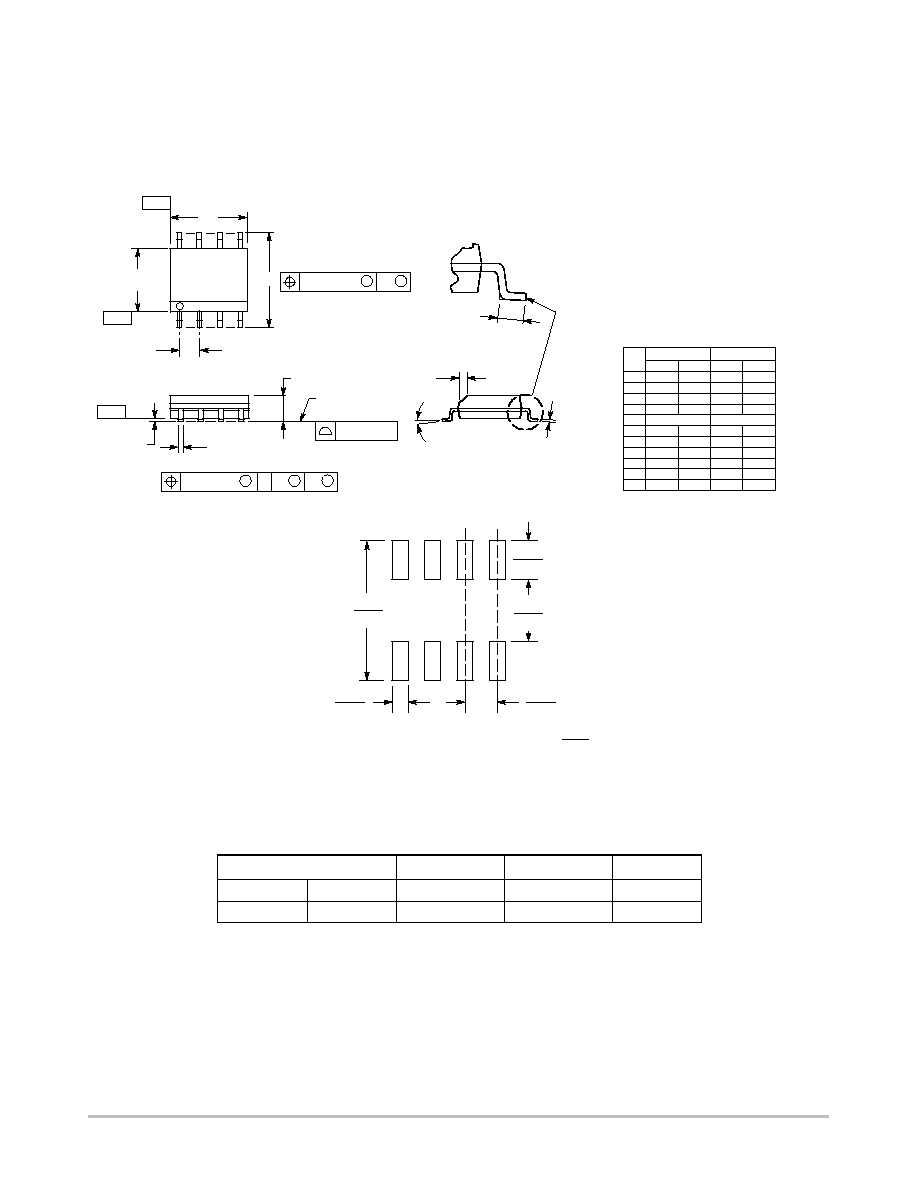
PACKAGE DIMENSIONS
D
2
PAK-5
DP SUFFIX
CASE 936AC-01
ISSUE O
For D
2
PAK Outline and
Dimensions - Contact Factory
CS5231-3
http://onsemi.com
13
PACKAGE DIMENSIONS
SOIC-8
DF SUFFIX
CASE 751-07
ISSUE AA
SEATING
PLANE
1
4
5
8
N
J
X 45
_
K
NOTES:
1. DIMENSIONING AND TOLERANCING PER ANSI
Y14.5M, 1982.
2. CONTROLLING DIMENSION: MILLIMETER.
3. DIMENSION A AND B DO NOT INCLUDE MOLD
PROTRUSION.
4. MAXIMUM MOLD PROTRUSION 0.15 (0.006) PER
SIDE.
5. DIMENSION D DOES NOT INCLUDE DAMBAR
PROTRUSION. ALLOWABLE DAMBAR
PROTRUSION SHALL BE 0.127 (0.005) TOTAL IN
EXCESS OF THE D DIMENSION AT MAXIMUM
MATERIAL CONDITION.
6. 751-01 THRU 751-06 ARE OBSOLETE. NEW
STANDARD IS 751-07.
A
B
S
D
H
C
0.10 (0.004)
DIM
A
MIN
MAX
MIN
MAX
INCHES
4.80
5.00
0.189
0.197
MILLIMETERS
B
3.80
4.00
0.150
0.157
C
1.35
1.75
0.053
0.069
D
0.33
0.51
0.013
0.020
G
1.27 BSC
0.050 BSC
H
0.10
0.25
0.004
0.010
J
0.19
0.25
0.007
0.010
K
0.40
1.27
0.016
0.050
M
0
8
0
8
N
0.25
0.50
0.010
0.020
S
5.80
6.20
0.228
0.244
-X-
-Y-
G
M
Y
M
0.25 (0.010)
-Z-
Y
M
0.25 (0.010)
Z
S
X
S
M
_
_
_
_
Figure 27. SOIC-8
1.52
0.060
7.0
0.275
0.6
0.024
1.270
0.050
4.0
0.155
mm
inches
SCALE 6:1
SOLDERING FOOTPRINT
PACKAGE THERMAL DATA
Parameter
D
2
PAK-5
SOIC-8
Unit
R
q
JC
Typical
2.5
25
∞
C/W
R
q
JA
Typical
10-50*
110
∞
C/W
*Depending on thermal properties of substrate. R
q
JA
= R
q
JC
+ R
q
CA
.

CS5231-3
http://onsemi.com
14
ON Semiconductor and are registered trademarks of Semiconductor Components Industries, LLC (SCILLC). SCILLC reserves the right to make changes without further notice
to any products herein. SCILLC makes no warranty, representation or guarantee regarding the suitability of its products for any particular purpose, nor does SCILLC assume any liability
arising out of the application or use of any product or circuit, and specifically disclaims any and all liability, including without limitation special, consequential or incidental damages.
"Typical" parameters which may be provided in SCILLC data sheets and/or specifications can and do vary in different applications and actual performance may vary over time. All
operating parameters, including "Typicals" must be validated for each customer application by customer's technical experts. SCILLC does not convey any license under its patent rights
nor the rights of others. SCILLC products are not designed, intended, or authorized for use as components in systems intended for surgical implant into the body, or other applications
intended to support or sustain life, or for any other application in which the failure of the SCILLC product could create a situation where personal injury or death may occur. Should
Buyer purchase or use SCILLC products for any such unintended or unauthorized application, Buyer shall indemnify and hold SCILLC and its officers, employees, subsidiaries, affiliates,
and distributors harmless against all claims, costs, damages, and expenses, and reasonable attorney fees arising out of, directly or indirectly, any claim of personal injury or death
associated with such unintended or unauthorized use, even if such claim alleges that SCILLC was negligent regarding the design or manufacture of the part. SCILLC is an Equal
Opportunity/Affirmative Action Employer. This literature is subject to all applicable copyright laws and is not for resale in any manner.
PUBLICATION ORDERING INFORMATION
N. American Technical Support: 800-282-9855 Toll Free
USA/Canada
Japan: ON Semiconductor, Japan Customer Focus Center
2-9-1 Kamimeguro, Meguro-ku, Tokyo, Japan 153-0051
Phone: 81-3-5773-3850
CS5231-3/D
LITERATURE FULFILLMENT:
Literature Distribution Center for ON Semiconductor
P.O. Box 5163, Denver, Colorado 80217 USA
Phone: 303-675-2175 or 800-344-3860 Toll Free USA/Canada
Fax: 303-675-2176 or 800-344-3867 Toll Free USA/Canada
Email: orderlit@onsemi.com
ON Semiconductor Website: http://onsemi.com
Order Literature: http://www.onsemi.com/litorder
For additional information, please contact your
local Sales Representative.