©
Semiconductor Components Industries, LLC, 2001
October, 2001 ≠ Rev. 6
1
Publication Order Number:
CS5305/D
CS5305
Three-Phase Synchronous
Switching Step-Down
Controller with Single
Wire Current Sharing
The CS5305 provides a low≠cost, single≠controller solution for the
low≠voltage, high≠current power needs of next≠generation
workstation and server processors. This IC provides high accuracy and
the industry's fastest transient response, reducing the need for large
banks of output capacitors and providing the most compact, reliable,
and economical power supply.
Since each phase's output voltage and current feed back to develop
the PWM ramp signal (enhanced V
2
TM
control), the CS5305 shares
output current accurately between phases. Accurate current sharing
means that the power supply design does not need to use power
components rated to handle mismatched current per phase. The
enhanced V
2
control compensates for variations in both line and load.
The IC's built≠in single wire current sharing capability allows easy
paralleling of multiple Voltage Regulator Modules (VRMs) based on
the CS5305. The paralleled VRMs use a shared bus to provide high
current and high reliability to multiple microprocessor workstations
or servers.
The CS5305 meets VRM 9.x specifications with its Power Good,
Enable, Differential Remote Sense, and single≠wire Current Share
features. The product fits server and workstation VRMs, and can be
used to power Embedded Processors. The IC provides the simplest,
lowest≠cost solution for any low voltage, high current power supply.
Features
∑
Enhanced V
2
Control Method
∑
VRM 9.x Compatible VID Codes
∑
Lossless Inductor Current Sensing
∑
Single Wire Active Current Sharing Between Converters
∑
Auto Master≠Slave Current Share Control Method
∑
Programmable 200 to 800 kHz Switching Frequency
∑
Programmable Adaptive Voltage Positioning
∑
Differential Remote Sense
∑
Pulse≠by≠Pulse Current Limit
∑
Master Hiccup Overcurrent Protection through Single
Wire Share Bus
∑
5≠Bit DAC with 1% Tolerance
∑
ENABL Input
∑
VRM 9.x≠Compliant Power Good Output
∑
Active Current Sharing During Soft Start
http://onsemi.com
Device
Package
Shipping
ORDERING INFORMATION
SO≠28L
27 Units/Rail
SO≠28L
1000 Tape & Reel
SO≠28L
DW SUFFIX
CASE 751F
1
28
1
28
PWRGDS
I
FB
SGND
CS
REF
V
CC
CS3
DRVON
CS2
GATE3
CS1
GATE2
ENABL
GATE1
R
OSC
GND
OCSET
V
ID0
I
OUT
V
ID1
SHARE
V
ID3
V
DRP
V
ID2
SCOMP
V
ID4
V
FB
PWRGD
COMP
PIN CONNECTIONS
CS5305GDW28
CS5305GDWR28
MARKING
DIAGRAMS
A
= Assembly Location
WL, L
= Wafer Lot
YY, Y
= Year
WW, W = Work Week
1
CS5305
AWLYYWW
28
CS5305
http://onsemi.com
2
APPLICATION DIAGRAMS
GH
GH
GH
GND
GATE1
GATE2
GATE3
DRVON
V
CC
SGND
PWRGDS
V
ID0
V
ID1
V
ID2
V
ID3
V
ID4
PWRGD
OCSET
R
OSC
ENABL
CS1
CS2
CS3
CS
REF
I
FB
I
OUT
SHARE
SCOMP
V
DRP
V
FB
COMP
CS5305
3.9 k
47 nF
12 k
3 k
.01
µ
F
22 nF
91 k
17 k
220
0.1
µ
F
220
12 k
◊
3
47 nF
◊
3
GND SENSE
POWERGOOD
V
OUT
SENSE
SHARE
V
ID4
V
ID3
V
ID2
V
ID1
V
ID0
60.4 k
NCP5351
ENABLE
V
CC
GL
PGND
IN
BST
SWN
1
µ
F
.47 nF
NTD
4302
◊
2
NTD
4302
◊
2
BAS40LT1
NCP5351
ENABLE
V
CC
GL
PGND
IN
BST
SWN
1
µ
F
NTD
4302
◊
2
BAS40LT1
NCP5351
ENABLE
V
CC
GL
PGND
IN
BST
SWN
1
µ
F
NTD
4302
◊
2
BAS40LT1
NTD
4302
◊
2
NTD
4302
◊
2
V
OUT
100
µ
F
◊
5
270 nH
470 nH
20 k
ENABLE
28.7 k
+12 V
2.2
µ
F
220 k
0.1
µ
F
6.2 V
GND
5.6 V
.47
µ
F
.47
µ
F
Figure 1. VRM 9.0, 60 A Converter
10
µ
F
◊
3
20
CS5305
http://onsemi.com
3
12 V
ENABLE
V
ID0
V
ID1
V
ID2
V
ID3
V
ID4
V
OUT
SENSE
V
OUT
GND
GND SENSE
POWERGOOD
SHARE
12 V
ENABLE
V
ID0
V
ID1
V
ID2
V
ID3
V
ID4
V
OUT
SENSE
V
OUT
GND
GND SENSE
POWERGOOD
SHARE
ENABLE
V
ID0
V
ID1
V
ID2
V
ID3
V
ID4
12 V
5.0 V
GND
V
OUT
POWERGOOD
1.5 k
Inductors & Resistors
represent distribution
impedances.
*
Figure 2. Two≠Converter System with Sharing
MAXIMUM RATINGS*
Rating
Value
Unit
Operating Junction Temperature
150
∞
C
Storage Temperature Range
≠65 to 150
∞
C
ESD Susceptibility (Human Body Model)
2.0
kV
Thermal Resistance, Junction≠to≠Case, R
JC
15
∞
C/W
Thermal Resistance, Junction≠to≠Ambient, R
JA
75
∞
C/W
JEDEC Moisture Sensitivity
Level 5
≠
Lead Temperature Soldering:
Reflow: (SMD styles only) Note 1.
230 peak
∞
C
1. 60 second maximum above 183
∞
C.
*The maximum package power dissipation must be observed.
MAXIMUM RATINGS
Pin Number
Pin Symbol
V
MAX
V
MIN
I
SOURCE
I
SINK
1
OCSET
7.0 V
≠0.3 V
1.0 mA
1.0 mA
2
R
OSC
7.0 V
≠0.3 V
1.0 mA
1.0 mA
3
ENABL
16 V
≠0.3 V
1.0 mA
1.0 mA
4≠6
CS1≠3
7.0 V
≠0.3 V
1.0 mA
1.0 mA
7
CS
REF
7.0 V
≠0.3 V
1.0 mA
1.0 mA
8
I
FB
7.0 V
≠0.3 V
1.0 mA
1.0 mA
9
I
OUT
7.0 V
≠0.3 V
10 mA
10 mA
10
SHARE
16 V
≠0.3 V
50 mA
1.0 mA
11
SCOMP
7.0 V
≠0.3 V
1.0 mA
1.0 mA
12
V
DRP
7.0 V
≠0.3 V
1.0 mA
1.0 mA
13
V
FB
7.0 V
≠0.3 V
1.0 mA
1.0 mA
14
COMP
7.0 V
≠0.3 V
10 mA
1.0 mA
15
PWRGD
16 V
≠0.3 V
1.0 mA
20 mA
CS5305
http://onsemi.com
4
MAXIMUM RATINGS (continued)
Pin Number
I
SINK
I
SOURCE
V
MIN
V
MAX
Pin Symbol
16≠20
V
ID4
≠V
ID0
16 V
≠0.3 V
1.0 mA
1.0 mA
21
PWRGDS
7.0 V
≠0.3 V
1.0 mA
1.0 mA
22
SGND
0.3 V
≠0.3 V
1.0 mA
1.0 mA
23
V
CC
16 V
≠0.3 V
N/A
0.4 A, 1.0
µ
s 100 mA DC
24
DRVON
7.0 V
≠0.3 V
10 mA
1.0 mA
25≠27
GATE 3≠1
16 V
≠0.3 V
0.1 A, 1.0
µ
s; 25 mA DC
0.1 A, 1.0
µ
s 25 mA DC
28
GND
N/A
N/A
0.4 A, 1.0
µ
s; 100 mA DC
N/A
ELECTRICAL CHARACTERISTICS
(0
∞
C < T
A
< 70
∞
C; 0
∞
C < T
J
< 125
∞
C; 9.5 V < V
CC
< 14 V; C
GATEX
= 100 pF,
C
COMP
= 0.01
µ
F, C
SCOMP
= 0.01
µ
F, C
VCC
= 0.1
µ
F, R
ROSC
= 32.4 k
, R
SHARE
= 60.4 k
, V(OCSET) = 0.54 V, DAC Code 01110; unless
otherwise stated.)
Parameter
Test Conditions
Min
Typ
Max
Unit
Voltage Identification DAC (0 = Connected to GND, 1 = Open (Pulled≠up to internal 3.3 V) or Pulled≠up to external voltage
3
13 V)
Accuracy (all codes)
VID code ≠ 125 mV
Connect VFB to COMP,
SGND < 55 mV,
Measure COMP ≠ SGND
±
1.0
%
V
ID4
V
ID3
V
ID2
V
ID1
V
ID0
V
ID
Maximum Voltage
1
1
1
1
1
DRVON < 1.0 V, GATE
X
< 1.0 V
FAULT Mode
V
1
1
1
1
0
1.100
0.965
0.975
0.985
V
1
1
1
0
1
1.125
0.990
1.000
1.010
V
1
1
1
0
0
1.150
1.015
1.025
1.035
V
1
1
0
1
1
1.175
1.040
1.050
1.061
V
1
1
0
1
0
1.200
1.064
1.075
1.086
V
1
1
0
0
1
1.225
1.089
1.100
1.111
V
1
1
0
0
0
1.250
1.114
1.125
1.136
V
1
0
1
1
1
1.275
1.139
1.150
1.162
V
1
0
1
1
0
1.300
1.163
1.175
1.187
V
1
0
1
0
1
1.325
1.188
1.200
1.212
V
1
0
1
0
0
1.350
1.213
1.225
1.237
V
1
0
0
1
1
1.375
1.238
1.250
1.263
V
1
0
0
1
0
1.400
1.263
1.275
1.288
V
1
0
0
0
1
1.425
1.287
1.300
1.313
V
1
0
0
0
0
1.450
1.312
1.325
1.338
V
0
1
1
1
1
1.475
1.337
1.350
1.364
V
0
1
1
1
0
1.500
1.361
1.375
1.389
V
0
1
1
0
1
1.525
1.386
1.400
1.414
V
0
1
1
0
0
1.550
1.411
1.425
1.439
V
0
1
0
1
1
1.575
1.436
1.450
1.465
V
0
1
0
1
0
1.600
1.460
1.475
1.490
V
0
1
0
0
1
1.625
1.485
1.500
1.515
V
0
1
0
0
0
1.650
1.510
1.525
1.540
V

CS5305
http://onsemi.com
5
ELECTRICAL CHARACTERISTICS (continued)
(0
∞
C < T
A
< 70
∞
C; 0
∞
C < T
J
< 125
∞
C; 9.5 V < V
CC
< 14 V; C
GATEX
= 100 pF,
C
COMP
= 0.01
µ
F, C
SCOMP
= 0.01
µ
F, C
VCC
= 0.1
µ
F, R
ROSC
= 32.4 k
, R
SHARE
= 60.4 k
, V(OCSET) = 0.54 V, DAC Code 01110; unless
otherwise stated.)
Parameter
Unit
Max
Typ
Min
Test Conditions
Voltage Identification DAC (0 = Connected to GND, 1 = Open (Pulled≠up to internal 3.3 V) or Pulled≠up to external voltage
3
13 V)
0
0
1
1
1
1.675
1.535
1.550
1.566
V
0
0
1
1
0
1.700
1.560
1.575
1.591
V
0
0
1
0
1
1.725
1.584
1.600
1.616
V
0
0
1
0
0
1.750
1.609
1.625
1.641
V
0
0
0
1
1
1.775
1.634
1.650
1.667
V
0
0
0
1
0
1.800
1.658
1.675
1.692
V
0
0
0
0
1
1.825
1.683
1.700
1.717
V
0
0
0
0
0
1.850
1.708
1.725
1.742
V
Input Threshold
V
ID4
, V
ID3
, V
ID2
, V
ID1
, V
ID0
1.00
1.25
1.5
V
Input Pull≠up Resistance
0 V < V
ID4
, V
ID3
, V
ID2
,V
ID1
,
V
ID0
< 3.3 V
25
50
100
k
Pull≠up Voltage
1.0 M
to GND
2.5
2.7
3.0
V
SGND Bias Current
SGND < 55 mV, All DAC Codes
10
20
40
µ
A
Power Good Output
Upper Threshold
Force PWRGDS≠SGND
SGND < 55 mV
1.876 (≠5%)
1.975
2.074 (+5%)
V
Lower Threshold
Force PWRGDS≠SGND
SGND < 55 mV
0.95
◊
(V
ID
≠ 125 mV)
or ≠2.6% from
nominal PWRGD
Threshold
0.975
◊
(V
ID
≠ 125 mV)
V
ID
≠ 125 mV
or +2.6% from
nominal
PWRGD
Threshold
V
V
ID4
V
ID3
V
ID2
V
ID1
V
ID0
1
1
1
1
0
0.926
0.951
0.975
V
1
1
1
0
1
0.950
0.975
1.000
V
1
1
1
0
0
0.974
1.000
1.025
V
1
1
0
1
1
0.998
1.024
1.050
V
1
1
0
1
0
1.021
1.048
1.075
V
1
1
0
0
1
1.045
1.073
1.100
V
1
1
0
0
0
1.069
1.097
1.125
V
1
0
1
1
1
1.093
1.122
1.150
V
1
0
1
1
0
1.116
1.146
1.175
V
1
0
1
0
1
1.140
1.170
1.200
V
1
0
1
0
0
1.164
1.195
1.225
V
1
0
0
1
1
1.188
1.219
1.250
V
1
0
0
1
0
1.211
1.243
1.275
V
1
0
0
0
1
1.235
1.268
1.300
V
1
0
0
0
0
1.259
1.292
1.325
V
0
1
1
1
1
1.283
1.316
1.350
V
0
1
1
1
0
1.306
1.341
1.375
V
CS5305
http://onsemi.com
6
ELECTRICAL CHARACTERISTICS (continued)
(0
∞
C < T
A
< 70
∞
C; 0
∞
C < T
J
< 125
∞
C; 9.5 V < V
CC
< 14 V; C
GATEX
= 100 pF,
C
COMP
= 0.01
µ
F, C
SCOMP
= 0.01
µ
F, C
VCC
= 0.1
µ
F, R
ROSC
= 32.4 k
, R
SHARE
= 60.4 k
, V(OCSET) = 0.54 V, DAC Code 01110; unless
otherwise stated.)
Parameter
Unit
Max
Typ
Min
Test Conditions
Power Good Output
0
1
1
0
1
1.330
1.365
1.400
V
0
1
1
0
0
1.354
1.389
1.425
V
0
1
0
1
1
1.378
1.414
1.450
V
0
1
0
1
0
1.401
1.438
1.475
V
0
1
0
0
1
1.425
1.463
1.500
V
0
1
0
0
0
1.449
1.487
1.525
V
0
0
1
1
1
1.473
1.511
1.550
V
0
0
1
1
0
1.496
1.536
1.575
V
0
0
1
0
1
1.520
1.560
1.600
V
0
0
1
0
0
1.544
1.584
1.625
V
0
0
0
1
1
1.568
1.609
1.650
V
0
0
0
1
0
1.591
1.633
1.675
V
0
0
0
0
1
1.615
1.658
1.700
V
0
0
0
0
0
1.639
1.682
1.725
V
Switch Leakage Current
V
CC
= 14 V, PWRGDS = 1.4 V
≠
≠
1.0
µ
A
Delay
PWRGDS low to PWRGD low
50
250
600
µ
s
Output Low Voltage
PWRGDS = 1.0 V,
I
PWRGOOD
= 4.0 mA
≠
0.15
0.4
V
Voltage Feedback Error Amplifier
V
FB
Bias Current
Note 2.
9.5
10.3
11.5
µ
A
Comp Source Current
COMP = 0.5 V to 2.0 V,
V
FB
= 1.6 V
15
30
60
µ
A
Comp Sink Current
COMP = 0.5 V to 2.0 V,
V
FB
= 1.0 V
15
30
60
µ
A
Transconductance
≠10
µ
A < I
COMP
< +10
µ
A, Note 3.
≠
32.0
≠
mmho
Output Impedance
Note 3.
≠
2.5
≠
m
Open Loop DC Gain
Note 3.
60
95
≠
dB
Unity Gain Bandwidth
COMP = 0.01
µ
F, Note 3.
≠
50
≠
kHZ
PSRR @ 1.0 kHz
Note 3.
≠
70
≠
dB
COMP Max Voltage
V
FB
= 0 V
2.4
2.7
≠
V
COMP Min Voltage
V
FB
= 1.6 V
≠
0.1
0.2
V
COMP Discharge Threshold
≠
0.15
0.2
0.25
V
Hiccup Latch Discharge Current
CSx ≠ CS
REF
= .05 V,
OCSET = 0.1 V,
COMP = 0.5 V
2.0
5.0
10
µ
A
Hiccup Charge / Discharge Ratio
≠
4.5
6.0
7.5
≠
2. The V
FB
Bias Current changes with the value of R
OSC
per Figure 5.
3. Guaranteed by design. Not tested in production.

CS5305
http://onsemi.com
7
ELECTRICAL CHARACTERISTICS (continued)
(0
∞
C < T
A
< 70
∞
C; 0
∞
C < T
J
< 125
∞
C; 9.5 V < V
CC
< 14 V; C
GATEX
= 100 pF,
C
COMP
= 0.01
µ
F, C
SCOMP
= 0.01
µ
F, C
VCC
= 0.1
µ
F, R
ROSC
= 32.4 k
, R
SHARE
= 60.4 k
, V(OCSET) = 0.54 V, DAC Code 01110; unless
otherwise stated.)
Parameter
Unit
Max
Typ
Min
Test Conditions
Voltage Feedback Error Amplifier
SHARE Fault Discharge Current
SHARE = 3.5 V,
COMP = 0.5 V,
CSx = CS
REF
= 0 V,
OCSET = 0.5 V
0.3
2.5
5.0
mA
Enable Input
Threshold Voltage
Monitor DRVON
1.12
1.25
1.38
V
Pull≠up Voltage
1 M
to GND
2.5
2.7
3.0
V
Input Pull≠up Resistance
≠
25
50
100
k
PWM Comparators
Minimum Pulse Width
Measured from CSx to GATEx,
V
FB
= CS
REF
= 0.5 V,
COMP = 0.5 V,
60 mV step on CSx;
measure at GATEx = 1.0 V
≠
75
220
ns
Transient Response Time
Measured from CS
REF
to GATEx,
COMP = 2.1 V,
CSx = CS
REF
= 0.5 V,
CS
REF
stepped
from 1.2 V ≠ 2.0 V
≠
100
150
ns
Channel Start≠up Offset
CSx = CS
REF
= V
FB
= 0 V,
measure V(COMP) when
GATEx switch high
0.34
0.6
0.75
V
Channel Start≠up Offset
Mismatch
CSx = CS
REF
= V
FB
= 0 V,
measure V(COMP) when
GATEx switch high, Note 4.
≠5.0
≠
5.0
mV
Gates
High Voltage
I
GATEx
= 1.0 mA
2.25
2.5
3.0
V
Low Voltage
I
GATEx
= 1.0 mA
≠
0.2
0.4
V
Rise Time GATE
0.8 V < GATE < 2.0 V,
V
CC
= 10 V
≠
15
30
ns
Fall Time GATE
2.0 V > GATE > 0.8 V,
V
CC
= 10 V
≠
15
30
ns
Oscillator
Switching Frequency
R
OSC
= 32.4 k
300
400
500
kHz
Switching Frequency
R
OSC
= 63.4 k
,
Note 4.
150
200
250
kHz
Switching Frequency
R
OSC
= 16.2 k
,
Note 4.
600
800
1000
kHz
R
OSC
Voltage
Note 4.
0.90
1.00
1.10
V
Phase Delay
≠
90
120
150
deg
4. Guaranteed by design. Not tested in production.

CS5305
http://onsemi.com
8
ELECTRICAL CHARACTERISTICS (continued)
(0
∞
C < T
A
< 70
∞
C; 0
∞
C < T
J
< 125
∞
C; 9.5 V < V
CC
< 14 V; C
GATEX
= 100 pF,
C
COMP
= 0.01
µ
F, C
SCOMP
= 0.01
µ
F, C
VCC
= 0.1
µ
F, R
ROSC
= 32.4 k
, R
SHARE
= 60.4 k
, V(OCSET) = 0.54 V, DAC Code 01110; unless
otherwise stated.)
Parameter
Unit
Max
Typ
Min
Test Conditions
Current Sense Amplifiers
CS
REF
Input Bias Current
CS
REF
= CSx = 0 V
≠
0.3
3.0
µ
A
CSx Input Bias Current
CS
REF
= CSx = 0 V
≠
0.1
1.0
µ
A
Sense Amp Gain
CS
REF
= 0 V, CSx = 0.05 V,
Measure V(COMP) when
GATEx switches high
.95
1.06
1.17
V / V
Mismatch
0
(CSx ≠ CS
REF
)
50 mV,
Note 5.
≠3.0
≠
3.0
mV
Common Mode Input Range
Note 5.
0
≠
2.0
V
Bandwidth
Note 5.
≠
7.0
≠
MHz
Single Phase Pulse by Pulse
Current Limit
V
FB
= CS
REF
= 0.5 V,
COMP = 2.0 V, Measure
CSx ≠ CS
REF
when GATEx
goes low
80
90
100
mV
OCSET Input Bias Current
OCSET = 0 V
≠
0.1
1.0
µ
A
Current Sense Input to OCSET
Gain
OCSET / R (CSx ≠ CS
REF
),
OCSET = 0.6 V,
Monitor DRVON < 1.0 V
3.4
3.7
4.0
V / V
Current Limit Filter Slew Rate
CS
REF
= 1.1 V, CSx = 1.0 V,
pulse CSx to 1.16 V, Note 5.
2.0
5.0
13
mV /
µ
s
Adaptive Voltage Positioning
V
DRP
Output Voltage to
DAC
OUT
Offset
CSx = CS
REF
, V
FB
= COMP,
Measure V
DRP
≠ COMP
≠30
2.0
60
mV
Maximum V
DRP
Voltage
CSx ≠ CS
REF
= 50 mV,
V
FB
= COMP,
Measure V
DRP
≠ COMP
500
560
620
mV
Current Sense Amp to V
DRP
Gain
CSx ≠ CS
REF
= 50 mV,
V
FB
= COMP,
Measure V
DRP
≠ COMP
3.4
3.7
4.0
V / V
V
DRP
Source Current
CSx ≠ CS
REF
= 50 mV,
V
FB
= COMP,
V
DRP
= 1.5 V
1.0
7.0
14
mA
SHARE Current Sense Amplifier
I
FB
Input Bias Current
I
FB
= 0 V
≠
0.2
1.0
µ
A
Input Offset Voltage
Note 5.
≠5.0
0
5.0
mV
Common Mode Input Range
Note 5.
0
≠
2.0
V
Output Current
I
OUT
= 0 V, CSx = 0.667 V,
CS
REF
= 0.5 V
1.0
10
22
mA
Gain
Note 5.
≠
120
≠
dB
Output Unity Gain BW
Note 5.
≠
5.0
≠
MHz
5. Guaranteed by design. Not tested in production.
CS5305
http://onsemi.com
9
ELECTRICAL CHARACTERISTICS (continued)
(0
∞
C < T
A
< 70
∞
C; 0
∞
C < T
J
< 125
∞
C; 9.5 V < V
CC
< 14 V; C
GATEX
= 100 pF,
C
COMP
= 0.01
µ
F, C
SCOMP
= 0.01
µ
F, C
VCC
= 0.1
µ
F, R
ROSC
= 32.4 k
, R
SHARE
= 60.4 k
, V(OCSET) = 0.54 V, DAC Code 01110; unless
otherwise stated.)
Parameter
Unit
Max
Typ
Min
Test Conditions
SHARE Bus
SHARE Amplifier Offset Voltage
Measure V(SHARE) ≠ V(I
OUT
),
0 < I
OUT
< 2.0 V
20
40
60
mV
SHARE Amplifier Source
Current
I
OUT
= 2.1 V, SHARE = 2.0 V
1.0
7.5
24
mA
SHARE Amplifier Max Voltage
I
OUT
= 3.5 V, T
A
= 25
∞
C
2.65
2.80
3.20
V
SHARE Fault Threshold
DRVON < 1.0 V, T
A
= 25
∞
C
3.2
3.4
3.7
V
SHARE OK Threshold
DRVON > 1.0 V
2.0
2.3
2.5
V
SHARE Fault Hysteresis
≠
1.0
1.15
1.3
V
SHARE Fault Output Voltage
≠
3.8
4.25
4.7
V
SHARE Fault Output Current
SHARE = 3.8 V
1.2
2.0
2.5
mA
SHARE Full Load Accuracy
CS
REF
= 0.5 V, CSx = 0.52 V,
I
OUT
/ FB Divider = 22 k
/3.0 k
1.7
1.95
2.2
V
SHARE Short Circuit Current
V(I
OUT
) = 2.0 V, SHARE = GND
1.0
17
28
mA
SHARE Fault Short Circuit
Current
CS
REF
= 0.5 V, CSx = 0.6 V
2.0
19
30
mA
Current SHARE Adjust Amplifier
Transconductance from I
OUT
to
SCOMP
0 < I
OUT
< 2.0 V,
0 < SCOMP < 2.0 V
23
40
53
µ
A / V
Gain from I
OUT
to COMP
Note 6.
30
50
140
mA / V
Maximum SCOMP source
current
SCOMP = 1.5 V
15
30
60
µ
A
Maximum SCOMP sink current
SCOMP = 1.5 V
15
30
60
µ
A
Unity Gain BW
C(SCOMP) = TBD, Note 6.
30
56
100
Hz
MOSFET Driver Enable
Pull≠Up Voltage
DRVON Floating
4.5
5.5
6.0
V
DRVON Source Current
DRVON = 1.5 V
.5
3.0
6.5
mA
DRVON Pull Down Resistor
DRVON = 1.5 V, ENABL = 0 V,
R = 1.5 V / I(1.5 V)
35
70
140
k
General Electrical Specifications
V
CC
Disable Current
ENABLE = 0 V (no switching)
≠
30
60
mA
UVLO Start Threshold
COMP charging, DRVON > 1.0 V
8.5
9.0
9.5
V
UVLO Stop Threshold
Gates not switching, COMP
discharging, DRVON < 1.0 V
7.5
8.0
8.5
V
UVLO Hysteresis
Start ≠ Stop
0.8
1.0
1.2
V
V
CC
Operating Current
ENABLE Open
≠
22
30
mA
6. Guaranteed by design. Not tested in production.

CS5305
http://onsemi.com
10
PACKAGE PIN DESCRIPTION
Package Pin Number
SO≠28L
Pin Symbol
Pin Name
Function
1
OCSET
Over≠Current Set
Resistor divider from R
OSC
to GND programs the threshold of the hiccup
over≠current protection.
2
R
OSC
Oscillator Frequency
Adjust
Resistance to GND programs the oscillator frequency. It also programs the V
FB
bias current shown in Figure 5.
3
ENABL
Enable Input
TTL≠Compatible logic input with 50 k
internal pull≠up resistor to 3.3 V. A logic
low puts the IC in FAULT mode.
4≠6
CS1≠3
Current Sense Inputs
Non≠inverting inputs to the current sense amplifiers.
7
CS
REF
Current Sense
Reference
Inverting input to the current sense amplifiers, and fast feedback input to the
PWM comparator.
8
I
FB
Share Current Amp
Inverting Input
Inverting input to share current amp. Connect resistor divider between I
OUT
, I
FB
,
and IC GND pin 28 to program Share Current Amp gain.
9
I
OUT
Share Current Amp
Output
Share current amplifier output and input to share adjust amplifier.
10
SHARE
Share Bus
Connect with other modules for single≠wire current sharing.
11
SCOMP
Share Compensation
Connect compensation network to stabilize share loop.
12
V
DRP
Current Sense Output
for AVP
The offset of this pin above the DAC voltage is proportional to the output current.
Connect a resistor from this pin to V
FB
to program the AVP voltage or leave this
pin open for no AVP.
13
V
FB
Voltage Feedback
Error Amp inverting input. Input bias current used to program AVP light load
offset via resistor connected to converter output voltage. Short V
FB
to the
converter output voltage for no AVP.
14
COMP
Error Amp Output and
PWM Comparator
Input
Provides loop compensation. Also used to control Softstart and Fault timing.
15
PWRGD
Power Good Output
Open collector output goes low when V
FB
is out of regulation. User must
externally limit current into this pin to less than 20 mA.
16≠20
V
ID4
≠V
ID0
Voltage ID DAC
Inputs
Programs Output Voltage. 50 k
internal pull≠up resistors to 3.3 V.
21
PWRGDS
Power Good Sense
Provides remote output voltage sensing.
22
SGND
Reference Ground
Ground connection for the DAC. Provides remote sensing of ground at the load.
23
V
CC
Supply Input
IC Power Supply Input.
24
DRVON
Driver Enable
Logic High enables outputs of compatible MOSFET Driver ICs. Low turns all
MOSFETs OFF. Pin driven from internal 5.5 V; 70 k
internal resistor to GND.
25≠27
GATE 3≠1
FET Driver Outputs
PWM Signal Input to external MOSFET Gate Driver ICs.
28
GND
Ground
IC Power Supply Return; connected to IC substrate.
CS5305
http://onsemi.com
11
V
ID0
V
ID1
V
ID2
V
ID3
V
ID4
DAC
SGND
50
k
-
+
3.3 V
OCSET
DAC OUTPUT
VID = 1
1111
?
OC Filter
-
+
- +
1.25 V
ENABL
ENABLE
Comparator
-
+
-
+
50 k
3.3 V
Start
Stop
-
+
V
CC
9.0 V
8.0 V
UVLO
Comparator
- +
-
+
-
+
0.2 V
Discharge
Comparator
Reset
Dominant
S
R
SHARE
Fault
* 0.975 V
-
+
- +
V
DRP
COMP
Reset
- +
-
+
PWM1
Comparator
ILIM1
Comparator
-
+
0.33
V
CO1
CO1F
- +
-
+
PWM2
Comparator
ILIM2
Comparator
-
+
0.33 V
CO2
CO2F
- +
-
+
PWM3
Comparator
ILIM3
Comparator
-
+
0.33 V
CO3
CO3F
Reset
Dominant
R
S
Reset
Dominant
R
S
Reset
Dominant
R
S
V
CC
PGND
PGND
V
CC
GA
TE2
GA
TE1
GA
TE3
Latch
PWM1
Latch
PWM2
Latch
PWM3
-
+
A
VP Amp
Delay
-
+
-
+
1.975 V
PWRGDS
PWRGD
-
◊
3.7
CO1
◊
1
CO1F
◊
3.7
CO2
◊
1
CO2F
◊
3.7
CO3
◊
1
CO3F
- +
- +
- +
- +
- +
CS
REF
CS1
CS2
CS3
-
+
-
+
SHARE Current Sense
Amp
-
+
30 mV
I
FB
I
OUT
SHARE Bus Amp
-
+
SHARE
Adjust Amp
SHARE
SCOMP
Start
Stop
-
+
-
+
3.1 V
2.1 V
SHARE Fault
Comparator
Error Amp
F
AUL
T
-
+
V
FB
-
+
0.6 V
-
+
3.3 V
-
+
3.8 V
SHARE
Fault
IBIAS
IDISCHG
F
AUL
T
COMP
Current Source
Generator
-
+
1.0 V
-
+
R
OS
C
PULSEOUT1
PULSEOUT2
PULSEOUT3
IOSC
OSCILLA
T
O
R
GND
F
AUL
T
5.5 V
DR
VON
70 k
OC
Comparator
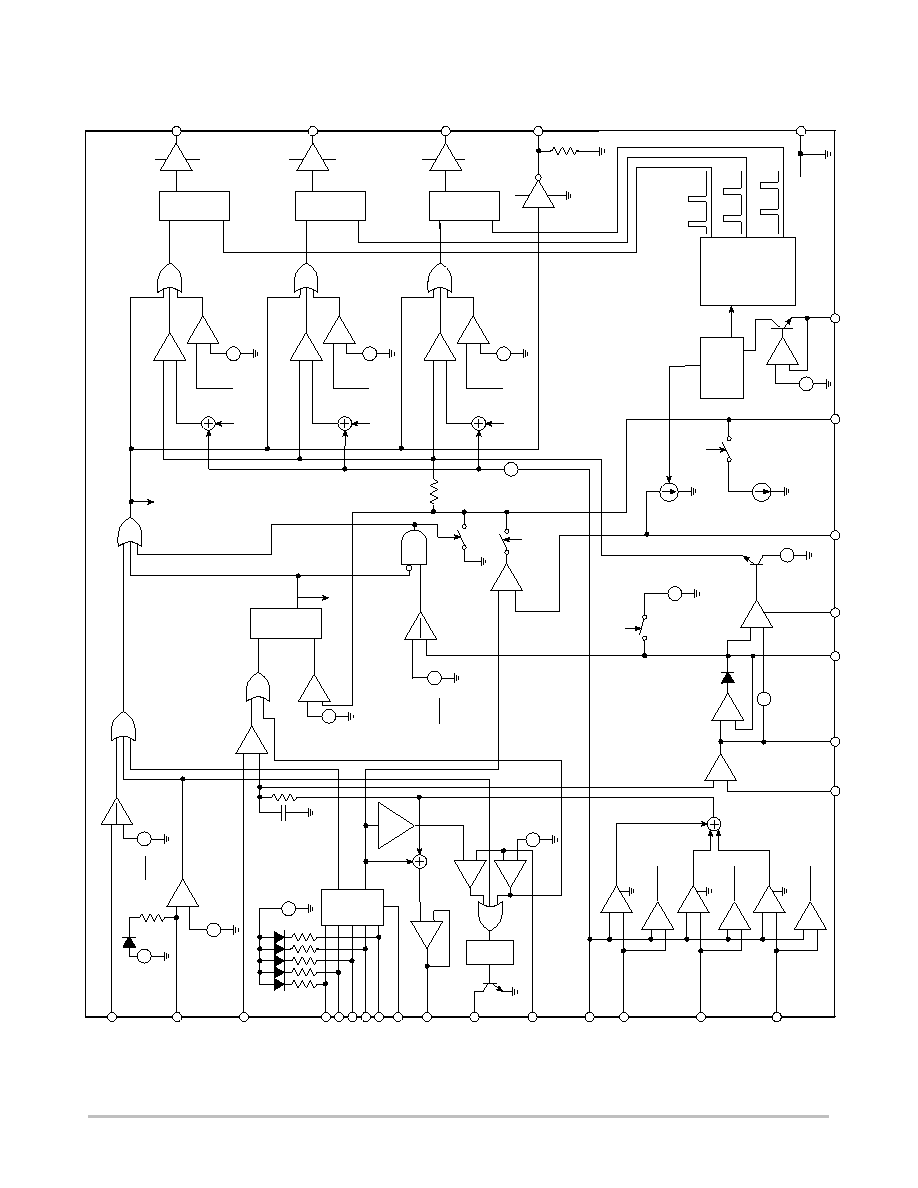
Figure 3. Block Diagram
V
CC
PGND
PGND
CS5305
http://onsemi.com
12
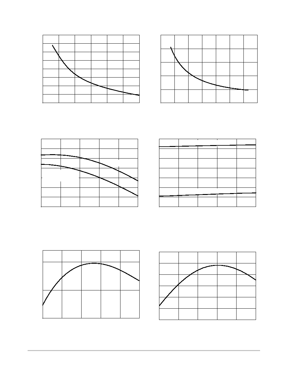
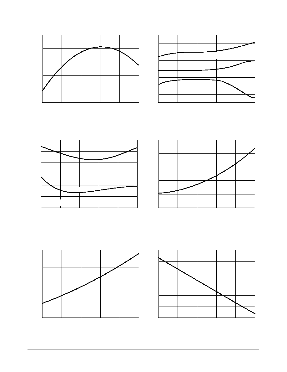
TYPICAL PERFORMANCE CHARACTERISTICS
Figure 4. Oscillator Frequency
0
I
CC
(mA)
33
Temperature (
∞
C)
34
35
36
37
38
39
40
25
50
75
100
125
ENABL = Low
ENABL = Floating
Gates Switching
0
Threshold V
oltage (V)
8.0
Temperature (
∞
C)
8.2
8.4
8.6
8.8
9.0
9.2
9.4
25
50
75
100
125
Start Threshold
Stop Threshold
0
Oscillator Frequency (kHz)
400
Temperature (
∞
C)
405
410
25
50
75
100
125
0
DAC Output (V)
1.348
Temperature (
∞
C)
1.349
1.350
1.351
1.352
1.353
1.354
25
50
75
100
125
Frequency (kHz)
100
R
OSC
Value (k
)
300
400
500
600
700
800
900
200
10
20
30
40
50
60
70
10
V
FB
Bias Current (
µ
A)
0
R
OSC
Value
5
10
15
20
25
20
30
40
50
60
70
80
Figure 5. V
FB
Bias Current vs. R
OSC
Value
Figure 6. I
CC
vs. Temperature
Figure 7. UVLO Start and Stop Thresholds vs.
Temperature
Figure 8. Oscillator Frequency vs. Temperature for
R
OSC
= 32.4 k
W
Figure 9. DAC Output for VID = 01111 (1.475 V)
CS5305
http://onsemi.com
13
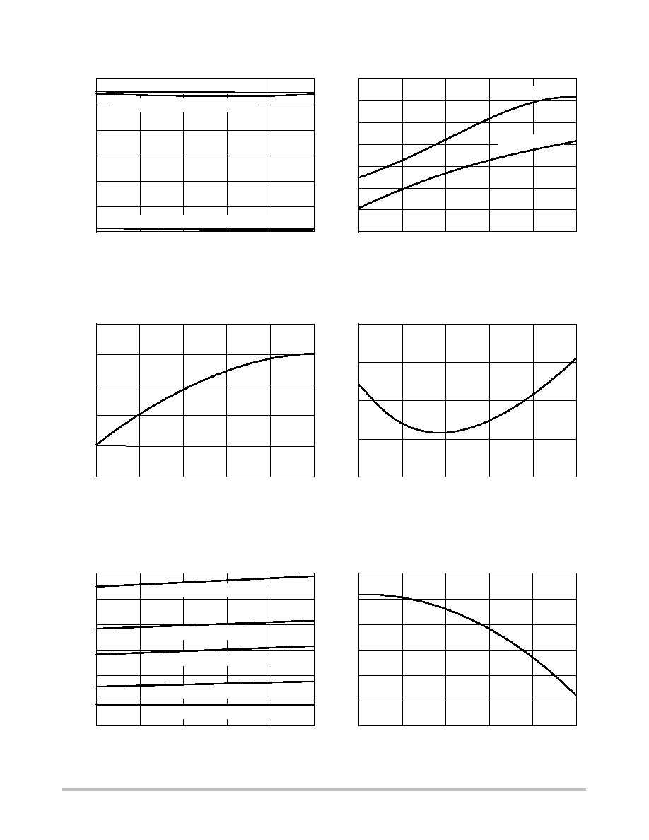
TYPICAL PERFORMANCE CHARACTERISTICS
Figure 10. DAC Output for VID = 00110 (1.700 V)
Figure 11. GATE Phase Delay vs. Temperature
Figure 12. GATE Rise and Fall Time vs. Temperature
Figure 13. PWM Comparator Minimum Pulse
Width vs. Temperature
Figure 14. PWM Transient Response Time vs.
Temperature
Figure 15. Current Sense Amp Channel Start≠Up
Offset Voltage vs. Temperature
0
DAC Output (V)
1.572
Temperature (
∞
C)
1.574
1.576
1.578
1.580
1.582
25
50
75
100
125
0
Phase Delay (degrees)
100
Temperature (
∞
C)
110
115
120
125
130
135
140
25
50
75
100
125
105
GATE3 to GATE1
GATE2 to GATE3
GATE1 to GATE2
0
Rise/Fall T
imes (ns)
4.0
Temperature (
∞
C)
6.0
8.0
10
25
50
75
100
125
Rise Time
Fall Time
0
Minimum Pulse Width (ns)
70
Temperature (
∞
C)
75
80
85
90
95
25
50
75
100
125
0
T
ransient Response T
ime (ns)
80
Temperature (
∞
C)
100
120
140
160
25
50
75
100
125
0
Start≠Up Of
fset V
oltage (mV)
400
Temperature (
∞
C)
450
500
550
600
650
700
25
50
75
100
125
C
LOAD
= 100 pF
CS5305
http://onsemi.com
14
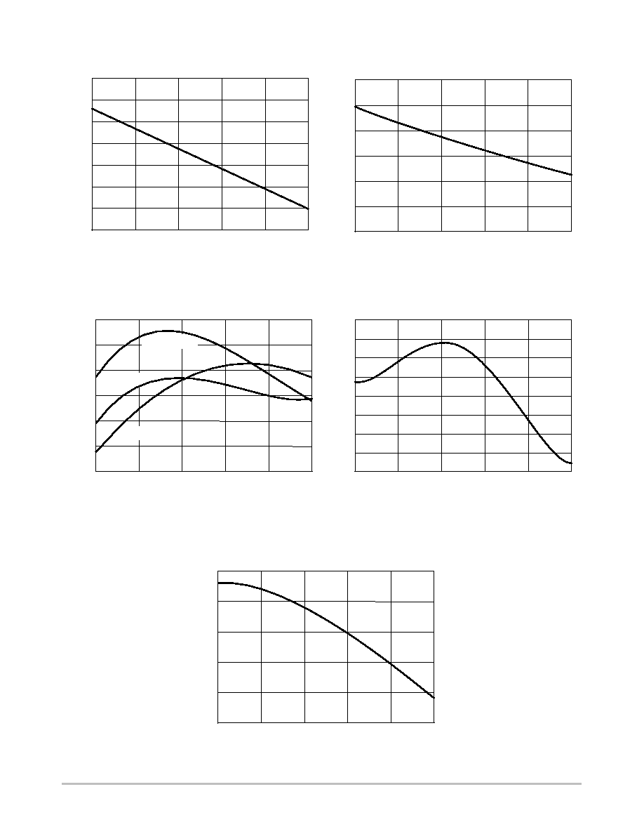
TYPICAL PERFORMANCE CHARACTERISTICS
Figure 16. Current Sense Amplifier Gain vs.
Temperature
Figure 17. V
FB
Bias Current vs. Temperature for
R
OSC
= 32.4 k
W
Figure 18. V
DRP
Source Current vs. Temperature
Figure 19. V
DRP
to DAC Output Offset Voltage vs.
Temperature
Figure 20. SHARE Bus Voltages vs. Temperature
Figure 21. I
OUT
Output Current vs. Temperature
0
Current
Sense Gain (V/V)
1.0
Temperature (
∞
C)
1.5
2.0
2.5
3.0
3.5
4.0
25
50
75
100
125
Current Sense Amp to V
DRP
Gain
Current Sense Amp to OSCETGain
Current Sense Amp to PWM Comparator Gain
0
V
FB
Bias Current (
µ
A)
10.55
Temperature (
∞
C)
10.60
10.65
10.70
10.75
10.80
10.85
10.90
25
50
75
100
125
V(V
FB
) = 1.9 V
V(V
FB
) = 1.0 V
0
V
DRP
Source Current (mA)
6.0
Temperature (
∞
C)
6.5
7.0
7.5
8.0
8.5
25
50
75
100
125
0
V
DRP
to DAC Output Of
fset V
oltage (mV)
0.8
Temperature (
∞
C)
1.0
1.2
1.4
1.6
25
50
75
100
125
0
SHARE Bus V
oltages (V)
1.5
Temperature (
∞
C)
2.0
2.5
3.0
3.5
4.0
4.5
25
50
75
100
125
SHARE Fault Output Voltage
SHARE Fault Threshold
SHARE Max Output Voltage
SHARE OK Threshold
SHARE Full Load Accuracy
0
I
OUT
Output Current (mA)
13.0
Temperature (
∞
C)
13.5
14.0
14.5
15.0
15.5
16.0
25
50
75
100
125
CS5305
http://onsemi.com
15
TYPICAL PERFORMANCE CHARACTERISTICS
Figure 22. SHARE Offset Voltage vs. Temperature
Figure 23. I
OUT
to S
COMP
Transconductance vs.
Temperature
Figure 24. Power Good Lower Threshold Voltage vs.
Temperature
Figure 25. Power Good Upper Threshold Voltage vs.
Temperature
Figure 26. Power Good Delay vs. Temperature
0
SHARE Of
fset V
oltage (mV)
38
Temperature (
∞
C)
39
40
41
42
43
44
45
25
50
75
100
125
0
I
OUT
to S
COMP
T
ransconductance (
µ
A/V)
15
Temperature (
∞
C)
20
25
30
35
40
45
25
50
75
100
125
0
Percentage Change Over Nominal (%)
≠0.06
Temperature (
∞
C)
≠0.04
≠0.02
0
0.02
0.04
0.06
25
50
75
100
125
VID = 11110
VID = 01110
VID = 00000
0
Power Good Upper Threshold V
oltage (V)
1.975
Temperature (
∞
C)
1.985
1.990
1.995
2.000
2.005
2.010
2.015
25
50
75
100
125
1.980
0
Power Good Delay (
µ
s)
210
Temperature (
∞
C)
215
220
225
230
235
25
50
75
100
125
CS5305
http://onsemi.com
16
APPLICATIONS INFORMATION
THEORY OF OPERATION
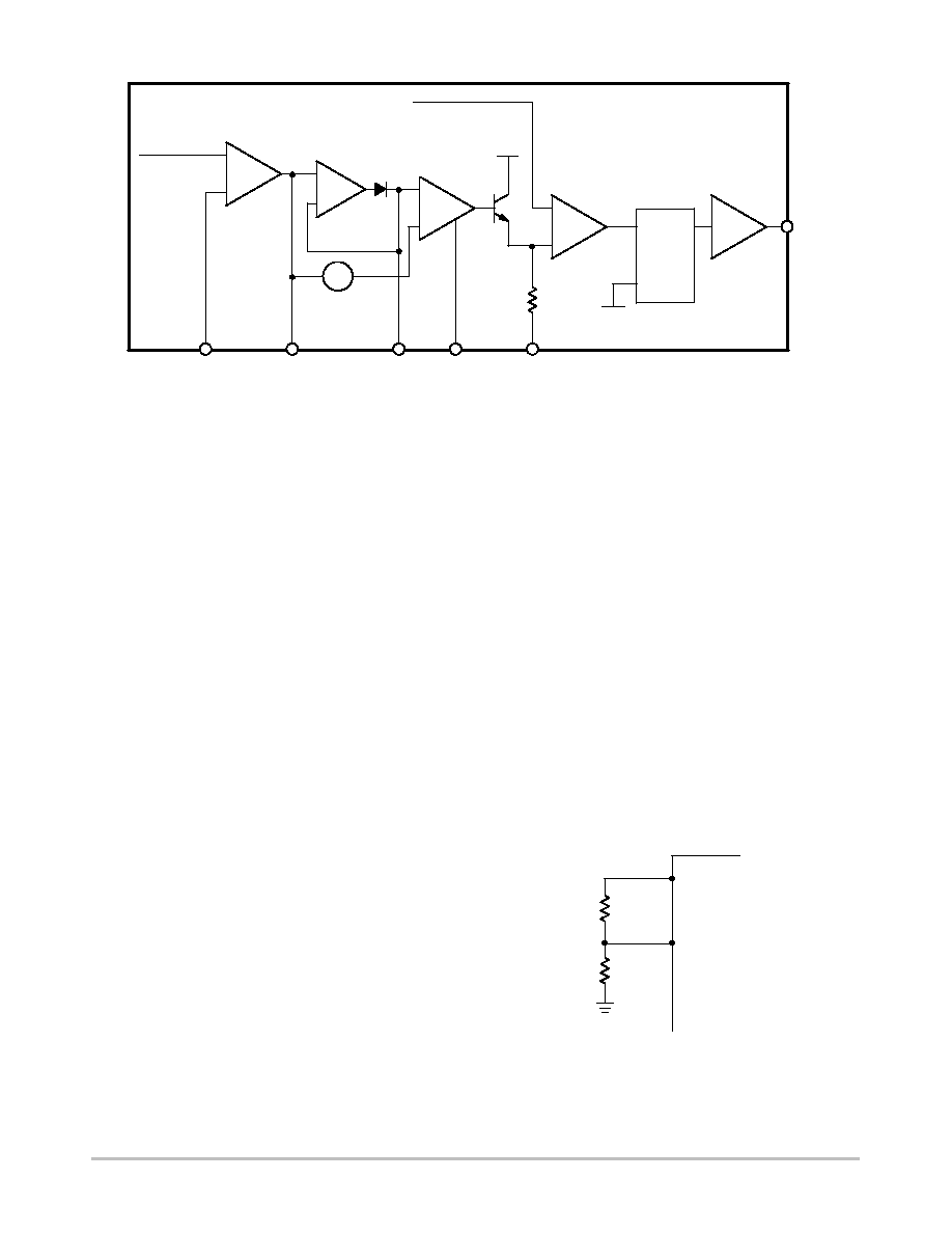
Fixed Frequency Multi≠phase Control
Multi≠phase CPU controllers include the necessary control
circuitry to implement several buck converters in parallel.
These converters are configured to turn on at different times.
This allows much higher output current than could be
provided by a single converter. The apparent ripple frequency
is increased and so output current can ramp up or down faster
than a single converter with the same value of output
inductor. Heat is also spread among multiple components.
The CS5305 uses a fixed frequency, Enhanced V
2
architecture. Each phase is delayed by approximately 120
∞
from the previous phase. The GATE output for each channel
changes to a logic high at the beginning of its oscillator cycle.
Inductor current ramps up until the combination of the current
sense signal and the output ripple trip the PWM comparator,
at which time the GATE output changes to a logic low. Once
low, the GATE output remains low until the next oscillator
cycle begins, and the control loop will not respond until that
time. The Enhanced V
2
control loop will respond to line and
load transients while the GATE output is high. Enhanced V
2
control will respond within the off time of the converter.
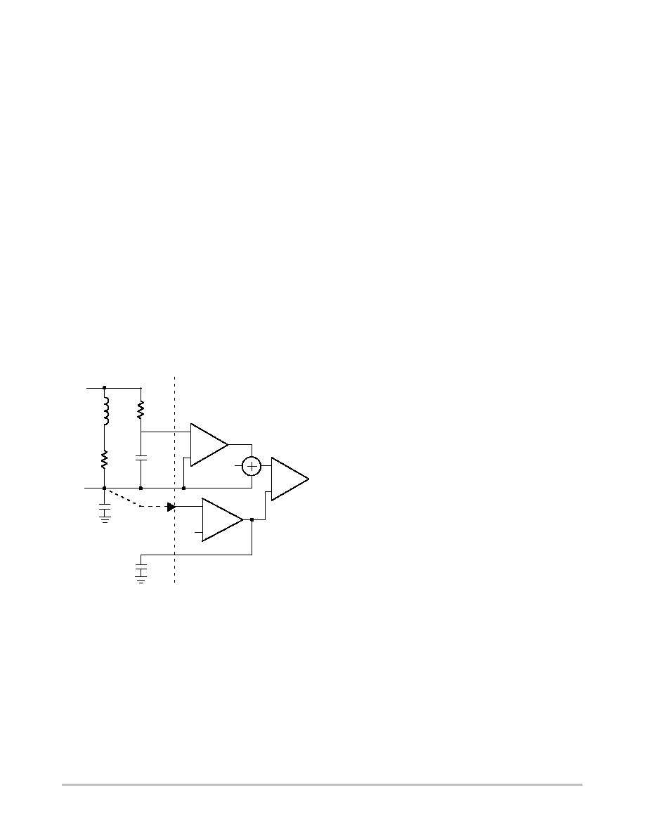
PWM
COMP
+
≠
OFFSET
CS AMP
+
≠
ERROR
AMP
≠
+
CSx
CS
REF
COMP
V
FB
R
CSx
C
CSx
C
COMP
L
ESR
L
SWITCH
V
OUT
NODE
Figure 27.
The Enhanced V
2
architecture measures and adjusts
current in each phase. An additional input (CSx pin)
provides current information for each output phase to the
control loop as shown in Figure 27. Inductor current is
measured across capacitor Ccsx. The voltage across this
capacitor is equal to the product of the output current and the
inductor ESR if these components are chosen such that
(Ccsx)(Rcsx) = (L)/ESR
L
. This signal is buffered by the
current sense amplifier (unity gain in the CS5305) and
summed with an offset voltage before it is presented as input
to non≠inverting input of the PWM comparator. Inductor
current provides the PWM ramp. As inductor current
increases, the voltage at the positive input to the PWM
comparator rises and terminates the PWM cycle. If the
inductor starts the next cycle with higher current, the PWM
cycle terminates earlier, thus providing negative feedback.
A CSx input is provided for each channel, but the CS
REF
,
V
FB
and COMP inputs are common to all phases. Current
sharing between phases is accomplished by referencing all
phases to the same error amplifier. Any phase with a larger
current signal will turn off earlier than the channels with a
lower current signal.
Including both current and voltage information in the
feedback signal allows the open loop output impedance of the
power stage to be controlled. In the absence of any load
current, the COMP pin voltage will be equal to the sum of the
output voltage, the offset voltage and half of the steady≠state
ramp voltage. (At no load, the output ripple current's positive
and negative contributions are equal, and the DC averaged
voltage is equal to half the ripple voltage.) If the COMP pin
is held steady and the inductor current is forced to change, the
output voltage will also change. In a closed≠loop situation,
changing the inductor current will force the COMP voltage to
change so the output voltage can remain the same. The change
in COMP voltage depends on the scaling of the current
feedback signal, and can be defined as:
D
VCOMP
+
(ESRL)(Current Sense Gain)(
D
IPHASE)
Since the current sense gain for this loop is unity, this
equation reduces to:
D
VCOMP
+
(ESRL)(
D
IPHASE)
and so the single≠phase power stage output impedance is:
D
VCOMP
D
IPHASE
+
ESRL
The CS5305 has three phases, so the total power stage
output impedance is then ESR
L
/3.
Lossless Inductive Current Sensing
Current can be sensed across the inductor as shown in
Figure 27. The output inductor is designated L and the
inductor's equivalent series resistance is designated ESR
L
.
In the ideal case, the values of Rcsx and Ccsx are chosen
such that (L/ESR
L
) = (Rcsx)(Ccsx). If this criterion is met,
the current sense signal will have the same shape as the
inductor current, and the circuit can be analyzed as if a sense
resistor with value equal to ESR
L
was placed in series with
the inductor. However, these components also determine the
ramp signal that is used to prevent pulse skipping and duty
cycle jitter. Choosing (Rcsx)(Ccsx) < (L/ESR
L
) will result
in the AC portion of the current sense signal being scaled
more than the DC portion. This results in a larger ramp
signal, but the current signal will overshoot during
transients. This will affect transient response, adaptive
voltage positioning and current limit. The COMP pin
voltage will overshoot along with the current signal in order
to maintain the output voltage. The COMP voltage will
CS5305
http://onsemi.com
17
eventually find the correct level for regulation, but the error
will decay with the time constant (Rcsx)(Ccsx). The V
DRP
voltage will also overshoot and response will be slowed,
since the current signal is a component of that voltage. The
single phase current limit will trip earlier since the current
signal appears larger than it should be, and the module
current limit will have a lower threshold for fast transients
than it will for slow transients. Additional external
components in the droop circuit and in the error amp
compensation will correct this condition. Details are provided
in the data sheet section on choosing external components.
Adaptive Voltage Positioning
Adaptive voltage positioning is a technique used to reduce
peak≠to≠peak output deviations during output current
transients. The output voltage is set higher than nominal at
light loads to reduce output voltage sag when load current is
suddenly increased. Similarly, output voltage is set lower
than nominal at heavy loads to reduce overshoot when load
current suddenly decreases. The CS5305 implements
adaptive voltage positioning by placing a resistor divider
between V
DRP
and V
OUT
. The center tap of the divider
connects to V
FB
. These resistors, along with two or three
other external components, implement a lossless droop
voltage function.
Past implementations of adaptive voltage positioning
used a droop resistor. This resistor was placed in series
between the regulation point of the output voltage and the
load. Increasing the current to the load caused the voltage at
the load to droop below the regulation point. The amount of
droop was equal to the change in current multiplied by the
droop resistor value. This method was acceptable for low
values of output current, where the droop resistor provided
a minimal change in voltage without dissipating a great deal
of power. Higher output current levels and tighter droop
voltage requirements in today's microprocessors have
rendered this droop resistor technique unusable. The
lossless technique solves these problems.
The AVP function addresses DC and slow transient output
voltage positioning. Response during the first few hundreds
of nanoseconds of a transient are addressed primarily by the
power stage output impedance, and the ESR and ESL of the
output filter. The ramp size and the error amplifier
compensation control the transition between these two
regions. If ramp size is too large or the error amp is too slow,
there will be a long transition to the final voltage after a
transient. This will be most apparent if the output
capacitance is low.
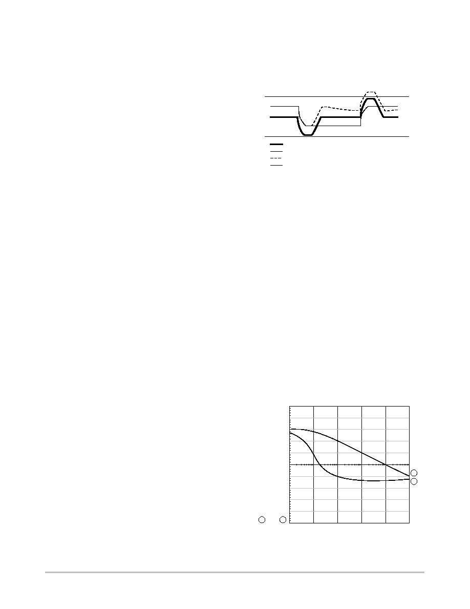
Figure 28 shows how adaptive positioning works. The
waveform labeled "normal" shows output voltage for a
converter without adaptive voltage positioning. The voltage
sags when current steps up, returns to its nominal value and
then overshoots when the current load is decreased. Using
a slow adaptive positioning circuit can actually worsen
performance. The slow adaptive positioning waveform
above shows the output voltage sag, but the voltage recovers
to its initial value before the adaptive positioning circuit
becomes active. When the load decreases, the overshoot
causes the output voltage to exceed the upper limit. The fast
adaptive positioning waveform shows how AVP can reduce
transient voltage requirements by about one half compared
to a "normal" converter.
Adaptive Positioning
Adaptive Positioning
Normal
Fast
Slow
Limits
Figure 28. Adaptive Positioning
Current Limit
The CS5305 features two separate current limit circuits.
First, the per≠phase current limit terminates topside switch
conduction in a phase if the voltage between any CSx pin
and CS
REF
exceeds a typical value of 90 mV. This provides
fast peak current protection for individual phases. In
addition, the output current signals for all three phases are
summed and filtered to provide an average module current
signal. This signal is compared to a voltage that is
user≠programmable. If this voltage is exceeded, the fault
latch is set and the COMP capacitor is discharged by a 5
µ
A
current sink until the COMP voltage falls below 0.2 V. The
soft≠start cycle begins when this threshold is reached, and the
converter will operate in hiccup≠mode until the overcurrent
condition is cleared.
Error Amplifier
The CS5305 uses the Enhanced V
2
control method to
offer the fastest and most accurate regulation available. One
of the features of this control method is ease of error
amplifier compensation. A single capacitor placed from the
COMP pin to ground is sufficient to adequately stabilize the
error amplifier.
200
160
120
80
40
100
60
20
≠20
≠60
V
DB
(VY2) in db(V
olts)
Phase(VY2) in Deg
100
1.0 k
10 k
100 k
Frequency in Hz
2
2
1
1
Figure 29. Error Amplifier Frequency
Response with No Compensation
CS5305
http://onsemi.com
18
80
40
0
≠40
≠80
170
150
130
110
90
Phase(VY1)
in Deg
+Result of V
DB
(VY1)
10
100
1.0 k
10 k
Frequency in Hz
Figure 30. Error Amplifier Frequency
Response with 0.1
m
F Capacitor
2
2
1
1
Soft Start/Hiccup Mode
At initial power≠up, the COMP voltage is zero. The total
COMP capacitance will begin to charge with a typical
current of 30
µ
A. (There may be more than one capacitor
connected between COMP and ground depending on the
adaptive voltage positioning compensation.) All GATE
outputs are held low until the COMP voltage reaches 0.6 V.
Once this threshold is reached, the GATE outputs are
released to operate normally. In hiccup≠mode, this will
result in GATE pulses being generated until the module
overcurrent condition reoccurs, and the discharge/Soft Start
cycle begins anew.
Undervoltage Lockout
The CS5305 includes an under≠voltage lockout circuit.
This circuit disables the output drivers until V
CC
applied to
the IC reaches a typical value of 9 V. The GATE outputs are
disabled when V
CC
drops below 8 V typical.
Enable
The CS5305 has a dedicated enable pin, in accordance with
the latest VRM specifications. This pin is internally pulled up
to a 3.3 V rail through a blocking diode and a 50 k
resistor.
The blocking diode allows external pull up to a bias voltage
greater than 3.3 V but below 13 V.
Fault Protection Logic
The CS5305 is equipped with sophisticated
fault≠detection and protection circuitry to ensure proper
operation in a paralleled VRM environment. In such an
environment, any one of several distinct failures could not
only destroy the VRM that sees the fault, but also those
VRMs that are connected in parallel with the faulted VRM.
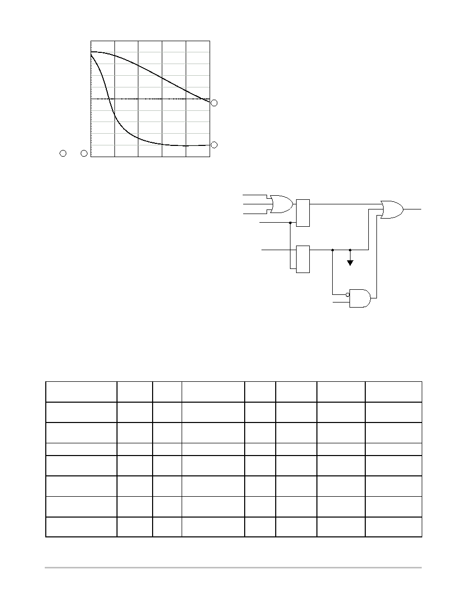
Table 1 describes the fault logic circuitry, shown below in
Figure 31.
VID FAULT
ENABLE
UVLO
S
R
COMP
DISCHG'D?
S
R
OVC
LOCAL
FAULT
LATCH
SHARE
FAULT
LATCH
SHARE
BUS
HIGH?
FAULT
SHARE
FAULT
Figure 31. Fault Logic Circuitry
Table 1. Description of Fault Logic
Fault Modes
Stop
Switching
DRVON
Level
PWRGD
Level
SHARE
Controller
Off
COMP Pin
Characteristics
Reset Method
Under Voltage Lockout
yes
low
low via Power Good
window comparator
n/a
no
≠5.0
µ
A
Comp < 0.2 V
VID = 11111
yes
low
low via Power Good
window comparator
n/a
no
≠5.0
µ
A
Comp < 0.2 V
Enable Low
yes
low
low
n/a
no
≠5.0
µ
A
Comp < 0.2 V
Module Over Current
(set by OCSET)
yes
low
low via Power Good
window comparator
> 3.8 V
no
≠5.0
µ
A
Comp < 0.2 V
Phase Over Current
(0.33 V limit)
terminate
pulse
high
n/a
n/a
no
not affected
not affected
External Share Fault
(SHARE > 3.8 V)
yes
low
low via Power Good
window comparator
n/a
no
≠2.5 mA
remove external
3.8 V from SHARE
PWRGDS out of win-
dow range
no
high
low
n/a
no
not affected
not affected
CS5305
http://onsemi.com
19
Gate Outputs
The CS5305 is designed to operate with external gate
drivers. Accordingly, the gate outputs are capable of driving
a 100 pF load with typical rise and fall time of 15 ns.
DRVON
When the CS5305 is used with DRVON≠compatible gate
drivers, the ability of the system to survive a fault in a
paralleled environment is greatly increased. The DRVON
signal tells the gate drivers to shut off both FETs while
entering a fault condition. This action takes the faulted VRM
"out of the picture," allowing the system to operate until the
bad module can be replaced.
Digital to Analog Converter (DAC)
The output voltage of the CS5305 module is set by means
of a 5≠bit, 1% DAC. The DAC pins are internally pulled up
to a 3.3 V rail through a blocking diode and a set of 50 k
resistors. The blocking diode allows external pull up to a
bias voltage greater than 3.3 V and less than 13 V.
The output of the DAC is described in the Electrical
Characteristics section of the datasheet. These outputs are
consistent with the latest VRM specifications. The DAC
produces an output voltage 125 mV lower than the VID code
would indicate in order to produce an accurate PWRGD
output. The relationship between the VID code and the DAC
code is described by Figure 32 shown below. The shaded
area shows the acceptable range of output voltages.
In order to produce a workable VRM using the CS5305,
the designer is expected to use AVP as described earlier to
position the output voltage above the DAC output, resulting
in an output voltage somewhere in the middle of the
acceptable range.
……………………
……………………
……………………
……………………
125 mV
VID code
DAC output
MAX V
OUT
MIN V
OUT
V
OUT
Figure 32. VRM 9.0 Output
Voltage Accuracy Requirements
The latest VRM specifications require a module to turn its
output off in the event of a 11111 VID code. When the DAC
sees such a code, the GATE pins stop switching and go low.
The DRVON signal also goes low, which turns off all FETs
on the module if the FET driver has an enable input. This
condition is described in Table 1.
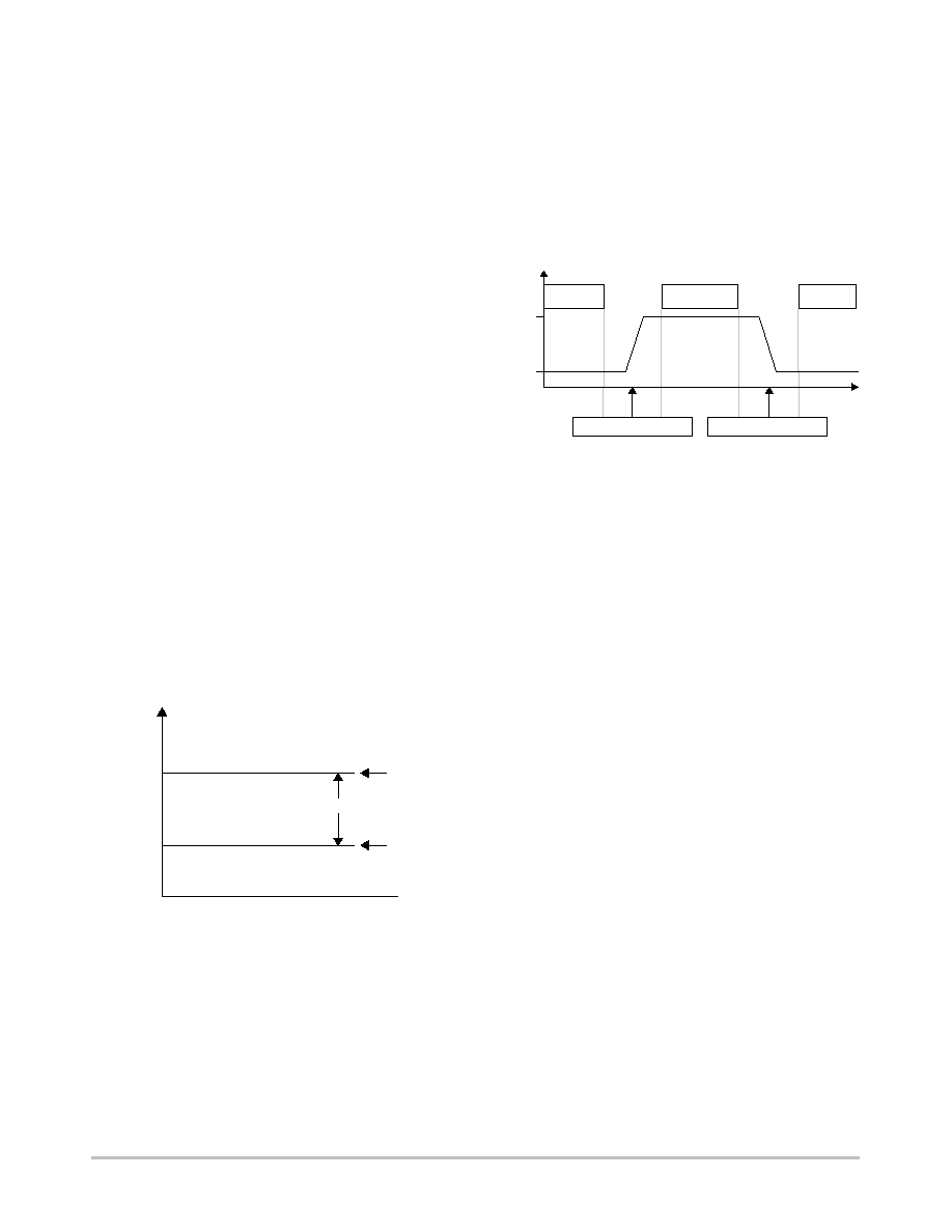
PWRGD
According to the latest VRM specifications, the PWRGD
signal is to be asserted when the output voltage is within a
window defined by the VID code, as shown in Figure 33.
PWRGD
………
………
«««
«««
«««
…………
…………
««««
««««
««««
0.975
◊
(VID ≠ 125 mV)
1.975 V
V
OUT
HIGH
LOW
PWRGD
≠2.6% +2.6%
≠5.0% +5.0%
Figure 33. PWRGD Assertion Window
low
PWRGD
low
PWRGD
high
In addition, certain fault modes must cause PWRGD to go
low to signal the system board that a VRM fault has
occurred. In that sense, the PWRGD signal operates as a
"VRM BAD" signal. These fault modes, as shown in Table 1
above, are ENABL low and CSx out of window.
When the ENABL pin is pulled low, PWRGD is pulled
low to indicate that the VRM is off. DRVON is pulled low
to turn both FETs off if the FET driver has an enable input.
The logic circuitry inside the chip sets PWRGD low only
after a delay period has been passed. A "power bad" event
does not cause PWRGD to go low unless it is sustained
through the delay time, typically 200
µ
s. If the anomaly
disappears before the end of the delay, the PWRGD output
will never be set low.
In order to use the PWRGD pin as specified, the user is
advised to connect external resistors as necessary to limit the
current into this pin to 4 mA or less.
Share Bus
VRM 9.x specifications require that a single≠wire share
bus be provided from each module. This bus allows output
current information to be communicated between modules
such that the total load current is shared equally by each
module. The CS5305 employs a proprietary share algorithm
called direct duty cycle control. A block diagram is provided
in Figure 34.
CS5305
http://onsemi.com
20
PWM
LATCH
RESET
SET
GATEx
GATE
DRIVER
+
≠
PWM
COMPARATOR
+
≠
+
≠
SHARE
BUS AMP
≠ +
30 mV
+
≠
SHARE
ADJUST AMP
SHARE
CURRENT
SENSE AMP
FROM
OSCILLATOR
COMP
SCOMP
SHARE
I
OUT
I
FB
3.7
◊
CURRENT
SENSE INPUT
3.3 V
V
OUT
+ V
OFFSET
+ 1
◊
CURRENT SENSE INPUT
Figure 34.
Direct duty cycle control utilizes a master≠slave approach
to current sharing. At any given current load, one module
will have a higher share bus voltage than the other modules.
This module acts as the master. It conveys output current
information to the other modules via the share bus. This
information is buffered and provided to the PWM
comparators, thus directly controlling duty cycle for the
slave modules.
The share current sense amplifier allows the user to
customize the share bus transconductance. Current sense
information is provided to the non≠inverting input from the
3.7
◊
current sense amplifier from each phase. This provides
a representation of the total module current. An external
resistor divider between I
OUT
and ground, center≠tapped at
I
FB
programs the share bus voltage for a particular current
level.
The share bus amplifier serves as a buffer and places the
I
OUT
voltage on the SHARE pin. Note there is a diode in the
schematic between the share bus amplifier and the SHARE
pin. This is an "ideal" diode, and indicates that the share bus
amplifier does not have current sink capability. This allows
the share bus to be driven by the module with the highest
share bus voltage. A 30 mV offset voltage provides noise
immunity to ensure that any given module does not cycle
between master and slave in a random fashion. It also
guarantees that the master module is not driving duty cycle
from the share bus. For the master module, the I
OUT
and
SHARE voltages will be equal. In this case, the 30 mV offset
holds the share adjust amplifier inactive, and the PWM
channel is controlled in the normal manner. The offset
voltage results in a current error between the master and
slave modules, but this error is small compared to the current
share tolerance found in the VRM 9.x specifications.
The share adjust amplifier takes the share bus voltage and
directly drives the PWM comparators of all slave modules
as previously described. The SCOMP pin provides a
connection point for a compensation capacitor for the share
adjust amplifier.
CHOOSING EXTERNAL COMPONENTS
FOR THE CS5305
R
OCSET
and R
OSC
The R
OSC
lead of the CS5305 provides a fixed 1 V
reference to the user. A resistive divider is connected from
R
OSC
to ground as shown in Figure 35. The center tap of the
divider is connected to the OCSET lead. The total
resistance from the R
OSC
lead to ground programs the
oscillator frequency for the converter according to the chart
in Figure 36.
The resistive divider also sets a voltage on the OCSET lead.
This voltage programs the module overcurrent trip point. The
module overcurrent comparator, or OC Comparator, uses the
OCSET lead voltage as the reference against which the
module output current signal is compared. The output current
of each phase is given as (V
CSx
≠ V
CSREF
) divided by the
equivalent series resistance of the inductor. The voltage
information (V
CSx
≠ V
CSREF
) is gained up by a factor of 3.7
and summed for all three phases at the non≠inverting input of
the OC Comparator. The fault latch is set if the module
overcurrent limit is exceeded. This results in "hiccup≠mode"
operation until the overcurrent condition is cleared.
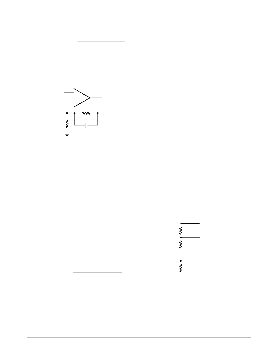
R1
R
OCSET
R
OSC
OCSET
R
OSC
= R1 + R
OCSET
Figure 35.
CS5305
http://onsemi.com
21
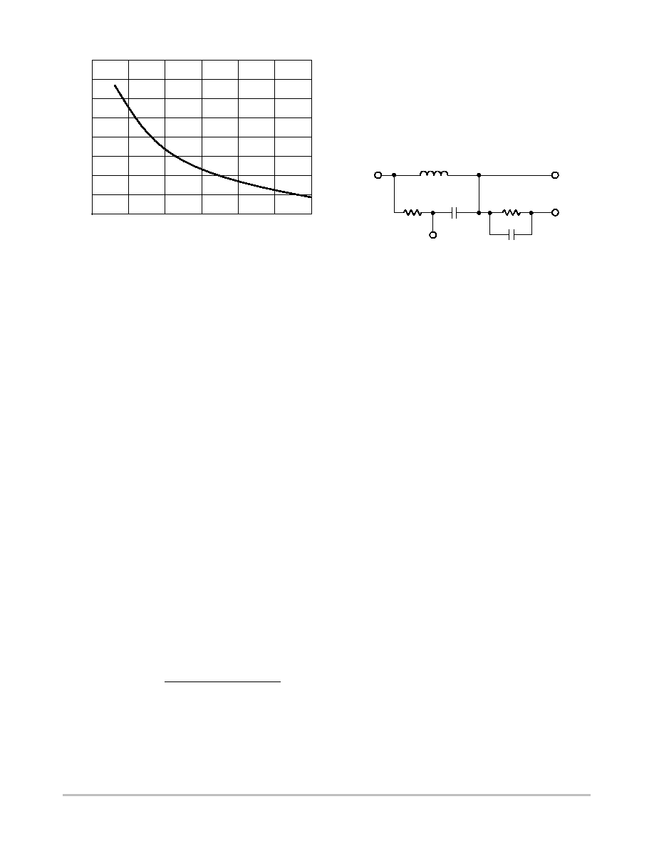
Figure 36. F
OSC
vs. R1 + R
OCSET
F
OS
C
(kHz)
100
R1 + R
OSCSET
(k
)
300
400
500
600
700
800
900
200
10
20
30
40
50
60
70
Additionally, the total value of resistance between R
OSC
and ground also programs the V
FB
pin bias current. V
FB
bias
current is equal to 0.333 V divided by the total resistance
from R
OSC
to ground. This current is used to generate the
droop function in the adaptive voltage positioning circuitry
and is discussed further in that section.
Current Sense Components
Current sense components are chosen for two reasons.
First, the value of R
CSx
and C
CSx
should be chosen to meet
the criterion:
(RCSx)(CCSx)
w
(L) (ESRL)
where L is the inductor value and ESR
L
is the inductor
equivalent series resistance. Meeting this criterion will
ensure that the module overcurrent limit is not exceeded
during current transients. Second, R
CSx
and C
CSx
should be
chosen to add a small amount of ramp to the system. This
will provide stable, jitter≠free operation. The amount of
ramp voltage required depends on several factors: supply
voltage, output voltage (DAC code), switching frequency
and board layout all affect the amount of artificial ramp
required to some degree. The power supply designer should
be aware that choosing the value of artificial ramp is a
trade≠off. As artificial ramp amplitude increases, the system
becomes less prone to duty cycle jitter, but transient
response will suffer. Adding 20 mV of artificial ramp is a
good compromise and can be used to start design.
The current sense ramp is generated from the square wave
obtained at the switching node of each phase by using an RC
filter. The RC filter components for the CSx leads should be
chosen to satisfy the following formula:
RCSx CCSx
v
(VOUT) 1
*
VOUT VCC
(fOSC)(VRAMP)
Choose a convenient standard value for C
CSx
and solve for
the value of R
CSx
. Each of the three output phases requires
its own RC combination.
An RC filter is also required for the CS
REF
connection.
This filter may use the same value of capacitance identified
for the CS1, CS2 and CS3 leads, but the value of resistance
should be one third that of R
CSx
:
RCSREF
+
RCSx 3
This change is necessary to compensate for the difference
in bias current between the CS
REF
lead and each CSx lead.
The schematic in Figure 37 shows the connection of these
components.
R
CSx
C
CSx
C
CSREF
R
CSREF
= R
CSx
/3
CS
REF
V
OUT
Switch
Node x
L1
CSx
Figure 37.
Share Bus Components
Five external components are required to implement the
module≠to≠module current share function. These
components
set the current sense load line, provide the share
bus pull≠down and compensate the share adjust amplifier.
The share current sense amplifier monitors the total
module current and provides a DC voltage output
proportional to that current. The share sense amplifier gain
is programmable and allows the user to set the share bus
transconductance. It is important that all modules in a
system have a share current load line that approximates that
of all the other modules to ensure accurate
module≠to≠module
current sharing. Let us arbitrarily set the
share bus maximum voltage for full load at 2 V. If a module
is designed to provide 81 A at full load, the module share
transconductance should be 81 A/2 V or 40.5 A/V. Two
resistors and a capacitor set the share current sense amplifier
gain. The resistors set the DC gain while the capacitor
provides a zero to minimize errors due to noise.
The total module current is measured as described in the
section dealing with the OCSET current limit function. That
is, each phase within a module generates a voltage between
the CSx and CS
REF
leads that is proportional to the current
flow in the output inductor and the inductor's ESR:
VCSx
*
VCSREF
+
(IL)(ESRL)
This signal is amplified by a factor of 3.7 for each phase
and then summed for all three phases. This signal is provided
as input to the share current sense amplifier. If we assume
that all three phases are sharing current equally within a
single module, the input to the share current sense amplifier
can be expressed as:
VIN(SENSE)
+
11.1(VCSx
*
VCSREF)
+
11.1(IL)(ESRL)
+
3.7(IOUT)(ESRL)
If we set I
L
equal to the maximum per phase current at full
load, and if we know the value of ESR for our inductors, we
CS5305
http://onsemi.com
22
can calculate the required share current sense amplifier
gain as:
AV(SHARESENSE)
+
share maximimum voltage
VIN(SENSE)
As an example, let us again consider the case for a module
providing full load current of 81 A. Each output phase is
conducting 27 A. If we assume ESR = 1.5 m
then input to
the share current sense amplifier is (11.1)(27 A)(1.5 m
) =
0.45 V. The required share current sense amplifier gain is
then 2 V/0.45 V = 4.44.
+
≠
R
IOUT
C
IOUT
I
FB
R
IFB
V
IN(SENSE)
I
OUT
Figure 38.
From the schematic in Figure 38, we derive the DC gain as:
AV(SHARESENSE)
+
4.44
+
RIOUT RIFB
)
1
This specifies that R
IOUT
should be 3.44 times greater than
R
IFB
.
Another important consideration is the type of resistor
selected for R
IFB
. The thermal performance of R
IFB
must
match that of whatever sense element is being used to monitor
module current. Inductive sensing has been shown to be
reasonably accurate, but copper's thermal coefficient of
resistivity is approximately +4000 parts per million per
∞
C
(0.4% per
∞
C). In order to maintain accurate control of the
share bus over temperature, R
IFB
must have a similar thermal
coefficient. This requires a positive temperature coefficient
element such as the KOA≠Speer LT73. If a standard sense
resistor is used in series between the inductor and the load,
there is no need to use special resistors for sensing, but
efficiency will suffer due to power dissipation in the sense
resistor.
As regards the value of C
IOUT
, it should be noted that the
complete transfer function for the share current sense
amplifier in Figure 38 is:
AV(SHARESENSE)
+
RIOUT
RIFB(1
)
sCIOUT RIOUT)
)
1
C
IOUT
causes the gain for high frequency noise to
decrease, thus quieting the share bus.
The share resistor provides a passive pull≠down on the
SHARE lead. This allows the share bus voltage to be pulled
all the way down to ground. The share resistor is selected to
satisfy a number of criteria. First, the resistor cannot be made
too small. The SHARE lead source current is guaranteed to
be above 1 mA and must be capable of driving the SHARE
lead voltage to 3 V. The share bus of one module serves as
master to all and drives the total resistance of all SHARE
leads. Thus, the total impedance of all share resistors should
be made greater than or equal to 3 k
. That is,
3 k
W w
RSHARE N
where N is the maximum number of modules that can be
placed in parallel as defined by the designer. As an
example, if ten is the maximum number of modules that
may be paralleled, then the minimum value of R
SHARE
should be 30 k
.
The share resistor should also not be made too large, since
this is the only pull≠down on the SHARE lead. Transient
response of the share bus is limited by the RC time constant
of the share resistance and any parasitic capacitance found
on the SHARE line between modules.
Droop Components
The CS5305 offers adaptive voltage positioning. This
feature allows the output voltage to be set at different levels
according to the amount of current being provided by the
module. The output voltage is somewhat higher than
nominal under no load or light load conditions and
somewhat lower than nominal under heavy load conditions.
Both set points must fall within the Power Good window.
The adaptive positioning allows for overshoot and
undershoot conditions that occur during load current
transients and results in a reduction in the peak≠to≠peak
V
OUT
voltage excursion during load current transients.
Three components are required to implement DC
adaptive voltage positioning. Resistor R
FB
is connected
between the module V
OUT(SENSE)+
lead and the V
FB
lead.
Resistor R
DRP
is connected between the V
DRP
lead and
V
FB
lead. Resistor R
VSENSE
is connected between the
V
OUT(SENSE)+
lead and the module V
OUT
lead. These
connections are shown in Figure 39.
Figure 39.
R
DRP
R
FB
R
VSENSE
V
OUT
V
OUT(SENSE)+
V
FB
V
DRP
The first step in choosing these components is to select the
appropriate no≠load and full≠load output voltage set points
for the particular DAC code being used. Additionally, the
values of R
OSC
and R
OCSET
should be known, as should
ESR of the output inductors and the full≠load output current.
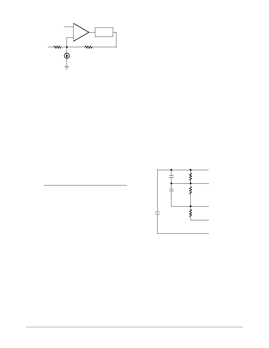
CS5305
http://onsemi.com
23
Figure 40.
+
≠
R
FB
V
DRP
V(DAC)
V
OUT
OUTPUT
STAGE
R
DRP
I(V
FB
)
V
FB
As was previously noted, the total value of resistance
between the R
OSC
pin and ground sets the V
FB
lead bias
current according to:
I(VFB)
+
0.333 V (ROSC
)
ROCSET)
Referring to Figure 40, the V
DRP
lead voltage is equal to
the DAC voltage plus the current sense information. Under
no load conditions, the V
DRP
and V
FB
pin voltages are equal,
and the entire V
FB
bias current flows between
V
OUT(SENSE)+
and V
FB
through R
FB
. Because the V
FB
bias
current sinks into V
FB
, the output voltage is forced to be
higher than the DAC voltage, and so the value of R
FB
can be
calculated as:
RFB
+
(VOUT no load set point
*
VDAC) I(VFB)
With R
FB
chosen, we can now select the value of R
DRP
.
If we again refer to Figure 40, we can use Kirchoff's
Current Law at the V
FB
node to find that the value of R
DRP
is defined as:
RDRP
+
(full load current)(3.7)(ESRL)(RFB)
(RFB)(I(VFB))
)
V(DAC)
*
VOUT full load set point
R
VSENSE
is used to ensure that a connection between
V
OUT
and V
OUT(SENSE)
always exists. This ensures that the
module will operate correctly in the event that the
V
OUT(SENSE)
connection is broken. The module≠to≠load
interface and the number of modules placed in parallel
determine the value of R
VSENSE
. The CS5305 is specified to
operate correctly with up to 55 mV dropped across the
module connector. It is assumed that the maximum current
allowed to flow in this connection to the load is 1 mA.
RVSENSE
+
55 mV (1 mA N)
where:
N = the number of modules to be paralleled.
If four modules are to be paralleled, each contributes a
maximum of 250
µ
A to this connection, and so R
VSENSE
=
55 mV/250
µ
A = 220
. This component is placed to ensure
the VRM module will regulate correctly if the module
V
OUT(SENSE)+
connection to the load is opened.
The transient droop performance should be checked next.
Performance should be verified using the transient test tool
typically provided in a microprocessor development kit.
True transient performance can be masked even at test
frequencies as low as 2 kHz. It should be possible to modify
the test tool so a function generator can drive it. Using lower
frequency (approximately 100 Hz) and lower duty cycle
(10%) allow the designer to better observe the true settling
behavior of the VRM module.
It may be necessary to add some filtering components to
the droop voltage divider. These components cause the AC
and DC gain from the current sense circuitry to match and
allow the user to tailor the droop output voltage
performance.
There
are two methods for tuning droop performance. The
first is illustrated in Figure 41. In this case, capacitors C
DRP
and C
FB
are placed in parallel with R
DRP
and R
FB
. A third
capacitor C
DRCMP
is connected between the COMP and
V
DRP
leads. The first two capacitors correct any gain errors
introduced in the selection of current sense components
Rcsx and Ccsx. Values for these components are defined as:
CFB
+
L ((RFB)(ESRL))
and
CDRP
+
((CCSx)(RCSx)) RDRP
The capacitor between V
DRP
and COMP allows the user
to fine≠tune the transition between "fast" AVP and the
slower positioning set by resistors R
DRP
and R
FB
. This
capacitor may or may not be required and is empirically
chosen based on the fine≠tuning procedure described below.
A value of 1 nF is recommended as an initial value.
Figure 41.
R
DRP
R
FB
R
VSENSE
V
OUT
V
OUT(SENSE)+
V
FB
V
DRP
C
DRP
C
FB
C
DRCMP
COMP
Set up the circuit to be tested with a DVM and
oscilloscope to the output. Have the scope set to DC input
and set its offset so a resolution of at least 100 mV/div is used
and the output is visible on the screen.
Using a DVM, measure the output voltage with no load.
If this value differs from the expected value, adjust R
FB
until
the nominal value is reached. Once this is set, mark this DC
level on the scope with a cursor.
Next, measure the output voltage with full DC load. If this
value deviates from the expected value, adjust R
DRP
until
the nominal value is reached. Once this is set, mark this DC
level on the scope with another cursor.
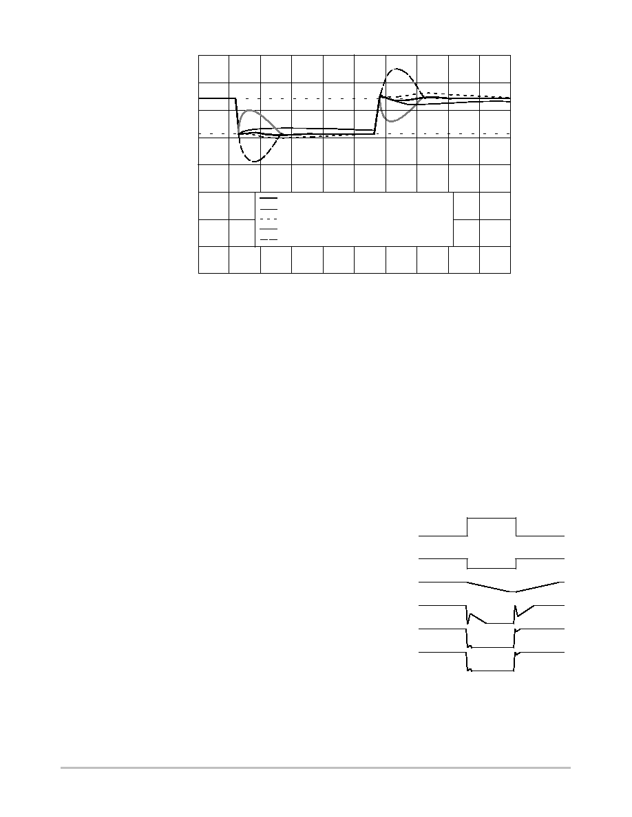
CS5305
http://onsemi.com
24
Figure 42.
No Load Cursor Marker
Full Load Cursor Marker
Trace 1: Optimal
Trace 2: C
FB
too large
Trace 3: C
FB
too small
Trace 4: C
DRCMP
too large, C
COMP
too small
Trace 5: C
DRCMP
too small, C
COMP
too large
Using the transient test tool, set up a current load step from
low current (1 A) to maximum load at the slew rate being
designed for. Set the current step at about 100 Hz with a duty
cycle of 10%. Converter response should be similar to that
shown in Figure 42.
Next, determine if there is a "bump" (trace 4 or trace 5) in
the output. Adjust C
COMP
and C
DRCMP
to flatten out this
bump. If the "bump" is negative (trace 5), make C
DRCMP
slightly larger and C
COMP
slightly smaller. If you see a
positive "bump" (trace 4), make C
DRCMP
slightly smaller
and C
COMP
slightly larger. If performance is better without
C
DRCMP
, just make C1 larger.
Once the bump is removed, look to see if the "pulse step"
magnitude is larger or smaller than the DC level (trace 2 or
trace 3). Make C
FB
slightly larger if the AC gain (trace 3) is
too large or slightly smaller if the AC gain (trace 2) is too
small. Once the output response resembles the "optimal"
trace (trace 1), the controller has been optimized for the
design from a static and dynamic response.
If the output appears to be jittering slightly prior to
optimizing transient response, make the previous
adjustments first, since they may solve the problem. If the
problem persists, decreasing the value of Rcsx across the
inductor will increase ramp amplitude, and jitter
performance should improve with increased ramp.
The second method uses a capacitor to "square up" the
COMP waveform and a series resistor and capacitor to tune
the V
DRP
waveform. These components are chosen
empirically based on observations of COMP and V
DRP
performance.
First, set the test tool for a load current transient from no
load (1 A) to full load and observe the COMP waveform.
The COMP waveform should ideally be flat, or at worst
decrease slightly during a current increase transient. The
principle at work here is that the increase in current sense
information will generate a voltage that should exactly
cancel the droop voltage, and thus the COMP capacitor
voltage should not change. In reality, it is unlikely that every
manufactured module can be built to perfectly compensate
the droop voltage, and so the COMP voltage should exhibit
a small amplitude square wave during transient conditions.
If the COMP voltage is decreasing gradually, the current
sense information is too small to fully compensate for the
droop voltage, and the designer should add a capacitor
between V
OUT
and COMP. This capacitor is chosen
empirically, with 1 nF a good starting point. This capacitor
will pull the COMP pin down initially and "square up" the
COMP waveform as shown in Figure 43.
Figure 43.
Current Transient
COMP Ideal Waveform
COMP Uncorrected
Waveform
V
OUT
Uncorrected
Waveform
COMP Corrected
Waveform
V
OUT
Corrected
Waveform
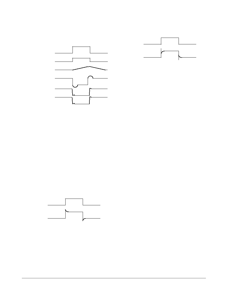
CS5305
http://onsemi.com
25
In a similar manner, if the current information is too large,
the COMP voltage will rise to compensate. Again, a square
wave is preferable to a slow change in the COMP voltage,
and placing a capacitor between V
DRP
and COMP will
"square up" the COMP waveform as shown in Figure 44.
Figure 44.
Current Transient
COMP Ideal Waveform
COMP Uncorrected
Waveform
V
OUT
Uncorrected
Waveform
COMP Corrected
Waveform
V
OUT
Corrected
Waveform
Once the COMP waveform has been squared up, it is
necessary to check the V
DRP
waveform. The V
DRP
waveform is dependent on the choice of ramp
components. If these components have been chosen such
that (R
CSx
)(C
CSx
) = L / ESR
L
, the V
DRP
waveform should
be a square wave that matches the current step. At this
point, the V
OUT
waveform should also be a square wave
and transient performance should be optimized.
If (R
CSx
)(C
CSx
) < L / ESR
L
, the V
DRP
waveform will be
faster than current step. The V
DRP
voltage will exhibit a fast
rise followed by an exponential droop down to a DC level,
as shown in Figure 45. This waveform has the effect of
telling the system that transient current signals are larger
than the true current. Response will be slowed, and V
OUT
will overshoot until the error amplifier "catches up". In this
case, it is desirable to push the V
FB
pin down, so that COMP
voltage is forced up and duty cycle is reduced slightly. This
is done by placing a series RC filter across resistor R
FB
.
Figure 45.
Current Step
V
DRP
(R
CSx
)(C
CSx
) < L/ESR
L
If (R
CSx
)(C
CSx
) > L / ESR
L
, the V
DRP
waveform will be
slower than the current step. V
DRP
will exhibit an initial
spike, but the voltage will then exponentially rise toward its
correct DC level, as shown in Figure 46. This waveform
effectively tells the system that the current signal is smaller
than the true current, and response will be faster than
optimal. V
OUT
will then undershoot. In this case, forcing
V
FB
up so COMP voltage decreases results in increasing
output duty cycle. The series RC filter is now located in
parallel with R
DRP
.
Figure 46.
Current Step
V
DRP
(R
CSx
)(C
CSx
) > L/ESR
L
These components are chosen empirically. The fastest
way to optimize the design is to start with a 1 nF capacitor
and a 500 k
potentiometer and "dial in" performance.
Error Amplifier Compensation
Error amplifier compensation is very simple using the
enhanced V
2
control architecture. A single 0.1
µ
F capacitor
from the COMP lead to ground is usually sufficient. As an
alternative, a resistor and capacitor in series between COMP
and ground may improve output voltage positioning during
current transients. The resistance will speed up the effective
slew rate of the error amplifier output.
The COMP capacitor also provides soft start and
hiccup≠mode timing. At start≠up, the COMP capacitance
must charge from ground through a typical channel start≠up
offset of 0.6 V before the GATE outputs are allowed to begin
switching. The COMP capacitance includes both the COMP
capacitor and any droop compensation capacitance that may
be connected to the COMP pin. The typical soft start time
can then be approximated as:
TSOFT≠START(ms)
+
20 CCOMP(TOTAL)(
m
F)
Hiccup timing has a similar equation. During
hiccup≠mode, the COMP voltage traverses between the
fault reset threshold (approximately 0.2 V) and the channel
start≠up offset voltage. When the fault circuitry becomes
active, the COMP capacitor is discharged with a 5
µ
A
current until the fault reset threshold is reached. The time
this initial discharge takes is variable depending on the
COMP voltage when the fault occurred. Once the reset
threshold is reached, the COMP capacitor is charged with
the 30
µ
A current until the start≠up offset voltage is reached.
The GATE outputs will begin to pulse, quickly ramping the
inductor current. The fault circuitry can then re≠detect the
fault condition some number of GATE pulses later if it is still
present. Thus, the period of the fault hiccup mode is
approximately defined as:
THICCUP(ms)
+
93.3 CCOMP(TOTAL)(
m
F)
Period is only approximately defined since the number of
GATE pulses between restart and redetection of a fault
condition is unpredictable.

CS5305
http://onsemi.com
26
Inductors
There are many factors to consider when choosing the
output inductors. Maximum load current, core and winding
losses, ripple current, short circuit current, saturation
characteristics, component height and cost are all variables
that the designer should consider. However, the most
important consideration in designing for the VRM 9.x
specifications may be the effect inductor value has on
transient response.
The amount of overshoot or undershoot exhibited during
a current transient is defined as the product of the current
step and the output filter capacitor ESR. To some degree,
adaptive voltage positioning is used to "pre≠position" the
output voltage so the voltage step during a current transient
will not cause the output voltage to exceed the Power Good
window. However, adaptive positioning will not completely
eliminate the overshoot or undershoot conditions, and
choosing the inductor value appropriately can minimize the
amount of energy that must be transferred from the inductor
to the capacitor or vice≠versa. In the subsequent paragraphs,
we will determine the minimum value of inductance
required for our system and consider the trade≠off of ripple
current vs. transient response.
In order to choose the minimum value of inductance, input
voltage, output voltage and output current must be known.
Most computer applications use reasonably well regulated
bulk power supplies so that, while the equations below
specify V
IN(MAX)
or V
IN(MIN)
, it is possible to use the
nominal value of V
IN
in these calculations with little error.
Current in the inductor while operating in the continuous
current mode is defined as the load current plus ripple
current.
IL
+
ILOAD
)
IRIPPLE
The ripple current waveform is triangular, and the current
is a function of voltage across the inductor, switch FET
on≠time and the inductor value. FET on≠time can be defined
as the product of duty cycle and switch frequency, and duty
cycle can be defined as a ratio of V
OUT
to V
IN
. Thus,
IRIPPLE
+
(VIN
*
VOUT)VOUT
(fOSC)(L)(VIN)
Peak inductor current is defined as the load current plus
half of the peak current. Peak current must be less than the
maximum rated FET switch current, and must also be less
than the inductor saturation current. Thus, the maximum
output current for a single phase can be defined as:
IOUT(MAX)
+
ISWITCH(MAX)
*
VIN(MAX)
*
VOUT VOUT
2 fOSC L VIN(MAX)
Since the maximum output current must be less than the
maximum switch current, the minimum inductance required
for a single phase can be determined.
L(MIN)
+
(VIN(MIN)
*
VOUT)VOUT
(fOSC)(ISWITCH(MAX))(VIN(MIN))
This equation identifies the value of inductor that will
provide the full rated switch current as inductor ripple
current, and will usually result in inefficient system
operation. The system will sink current away from the load
during some portion of the duty cycle unless load current is
greater than half of the rated switch current. Some value
larger than the minimum inductance must be used to ensure
the converter does not sink current. Choosing larger values
of inductor will reduce the ripple current, and inductor value
can be designed to accommodate a particular value of ripple
current by replacing I
SWITCH(MAX)
with a desired value of
I
RIPPLE
:
L(RIPPLE)
+
(VIN(MIN)
*
VOUT)VOUT
(fOSC)(IRIPPLE)(VIN(MIN))
However, reducing the ripple current will cause transient
response times to increase. The response times for both
increasing and decreasing current steps are shown below.
TRESPONSE(INCREASING)
+
(L)(
D
IOUT)
(VIN
*
VOUT)
TRESPONSE(DECREASING)
+
(L)(
D
IOUT)
(VOUT)
Inductor value selection also depends on how much output
ripple voltage the system can tolerate. Output ripple voltage
is defined as the product of the output ripple current and the
output filter capacitor ESR. However, since the CS5305 has
three paralleled phases, the net effect is that the switching
frequency as seen by the output capacitance is tripled relative
to the CS5305 operating frequency. This is because each
phase switches in sequence and the ripple currents in each
phase are superimposed on the output capacitance. This is
illustrated graphically in Figures 45 and 46.
Thus, output ripple voltage can be calculated as:
VRIPPLE
+
ESRC IRIPPLE
+
ESRC VIN
*
VOUT VOUT
3 fOSC L VIN
It is also important to note that the maximum value of
inductor ESR is limited by the single≠phase pulse≠by≠pulse
current limit. The specified minimum value for this
parameter is 80 mV, so the maximum inductor ESR is:
ESRL(MAX)(in ohms)
+
(0.08 V)
single phase current limit value in Amps
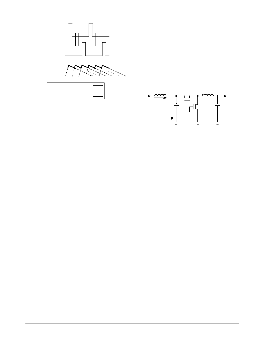
CS5305
http://onsemi.com
27
Figure 47.
PHASE 1 SWITCH NODE
PHASE 2 SWITCH NODE
PHASE 3 SWITCH NODE
SUPERIMPOSED PHASE
INDUCTOR CURRENTS
PHASE 1 CURRENT
PHASE 2 CURRENT
PHASE 3 CURRENT
OUTPUT RIPPLE CURRENT
Finally, we should consider power dissipation in the
output inductors. Power dissipation is proportional to the
square of inductor current:
PD
+
I
2
PHASE
)(ESRL)
The temperature rise of the inductor relative to the air
surrounding it is defined as the product of power dissipation
and thermal resistance to ambient:
D
T(inductor)
+
(Ra)(PD)
Ra for an inductor designed to conduct 20 A to 30 A is
approximately 45
∞
C/W. The inductor temperature is given as:
T(inductor)
+ D
T(inductor)
)
Tambient
Output Filter Capacitors
Each microprocessor manufacturer specifies output filter
capacitors for the motherboards. In addition, the designer
may need to add some output capacitance on the VRM
module. These added output capacitors would serve to
reduce the noise floor and help ensure jitter≠free operation.
If needed, one or two ceramic capacitors should be
sufficient. They should have a 4 WVDC rating. Large
amounts of bulk capacitance placed on the VRM module are
not useful, since the impedance of the VRM connector exists
between the module and the load. Low equivalent series
resistance is important since output ripple voltage and
response to output current transients are largely dependent
on this parasitic parameter.
V
CC
Bypass Filtering
A small RC filter should be added between module V
CC
and
the V
CC
input to the CS5305. A 10
resistor and a 0.1
µ
F
capacitor should be sufficient to ensure the controller IC does
not operate erratically due to injected noise.
Module Input Filter Capacitors
The input filter capacitors for the VRM module provide
a charge reservoir that minimizes supply voltage variations
due to changes in current flowing through the switch FETs.
These capacitors must be chosen primarily for ripple current
rating.
Figure 48.
V
IN
V
OUT
I
IN(AVE)
I
RMS(CIN)
C
IN
CONTROL
INPUT
L
IN
L
OUT
C
OUT
Consider the schematic shown in Figure 48. The average
current flowing in the input inductor L
IN
for any given
output current is:
IIN(AVE)
+
(IOUT)(VOUT VIN)
+
(IOUT per phase)(n)(D)
where:
D = duty cycle,
n = number of phases.
Input capacitor current is positive into the capacitor when
the switch FETs are off, and negative out of the capacitor
when the switch FETs are on. When the switches are off,
I
IN(AVE)
flows into the capacitor. When the switches are on,
capacitor current is equal to the per≠phase output current
minus I
IN(AVE)
. If we ignore the small current variation due
to the output ripple current, we can approximate the input
capacitor current waveform as a square wave. We can then
calculate the RMS input capacitor ripple current:
IRMS(CIN)
+
I
2
IN(AVE)
)
D
n
IOUT per phase
*
IIN(AVE) 2
*
I
2
IN(AVE)

CS5305
http://onsemi.com
28
The input capacitance must be designed to conduct the
worst case input ripple current. This will require several
capacitors in parallel. In addition to the worst case current,
attention must be paid to the capacitor manufacturer's
derating for operation over temperature.
As an example, let us define the input capacitance for a
12 V to 1.7V conversion at 81 A, or 27 A per phase at an
ambient temperature of 60
∞
C. A droop voltage of 90 mV to
1.61 V and efficiency of 80% is assumed. Average input
current in the input filter inductor is:
IIN(AVE)
+
(27 A)(3 phases)(1.61 V 12 V)
80%
+
10.868 A
Input capacitor RMS ripple current is then
IIN(RMS)
+
10.8682
)
1.61 V
12 V
3
27 A
*
10.868 A 2
*
10.868 A2
+
13.347 A
If we consider a Sanyo SP series capacitor, the ripple
current rating for a 16SPS100M capacitor is 2820 mA at
100 kHz and 45
∞
C. The derating factor is 0.85 for operation
up to 65
∞
C, resulting in an effective ripple current rating of
2397 mA. We determine the number of input capacitors by
dividing the ripple current by the per≠capacitor current
rating:
Number of capacitors
+
13.347 A 2.397 A
+
5.52
A total of at least 6 capacitors in parallel must be used to
meet the input capacitor ripple current requirements.
Output Switch FETs
Output switch FETs must be chosen carefully, since their
properties vary widely from manufacturer to manufacturer.
The CS5305 system is designed assuming that a FET driver
IC and n≠channel FETs will be used. The FET
characteristics of most concern are the gate
charge/gate≠source threshold voltage, gate capacitance,
on≠resistance, current rating and the thermal capability of
the package.
FET driver ICs have a limited drive capability. If the
switch FET has a high gate charge, the amount of time the
FET stays in its ohmic region during the turn≠on and
turn≠off transitions is larger than that of a low gate charge
FET, with the result that the high gate charge FET will
consume more power. Similarly, a low on≠resistance FET
will dissipate less power than will a higher on≠resistance
FET at a given current. Thus, low gate charge and low
R
DS(ON)
will result in higher module efficiency and will
reduce heat being generated by the VRM module.
It can be advantageous to use multiple switch FETs to
reduce power consumption. By placing a number of FETs in
parallel, the effective R
DS(ON)
is reduced, thus reducing the
ohmic power loss. However, placing FETs in parallel
increases the gate capacitance so that switching losses
increase. As long as adding another parallel FET reduces the
ohmic power loss more than the switching losses increase,
there is some advantage to doing so. However, at some point
the law of diminishing returns will take hold, and a marginal
increase in efficiency may not be worth the board area
required to add the extra FET. Additionally, as more FETs
are used, the limited drive capability of the FET driver will
have to charge a larger gate capacitance, resulting in
increased gate voltage rise and fall times. This will affect the
amount of time the FET operates in its ohmic region and will
increase power dissipation.
The following equations can be used to calculate power
dissipation in the switch FETs.
For ohmic power losses due to R
DS(ON)
:
PON(TOP)
+
(RDS(ON)(TOP))(IRMS(TOP))2(n)
(number of topside FETs per phase)
PON(BOTTOM)
+
RDS(ON)(BOTTOM) IRMS(BOTTOM) 2 n)
number of bottom≠side FETs per phase
where:
n = number of phases.
Note that R
DS(ON)
increases with temperature. It is good
practice to use the value of R
DS(ON)
at the FET's maximum
junction temperature in the calculations shown above.
IRMS(TOP)
+
I
2
PK
*
(IPK)(IRIPPLE)
)
D
3
I
2
RIPPLE
IRMS(BOTTOM)
+
I
2
PK
*
(IPKIRIPPLE)
)
(1
*
D)
3
I
2
RIPPLE
IRIPPLE
+
(VIN
*
VOUT)(VOUT)
(fOSC)(L)(VIN)
IPEAK
+
ILOAD
)
IRIPPLE
2
+
IOUT
3
)
IRIPPLE
2
where:
D = Duty cycle.
For switching power losses:
PD
+
nCV2(fOSC)
where:
n = number of switch FETs (either top or bottom) per phase,
C = FET gate capacitance,
V = maximum gate drive voltage (usually V
CC
),
f
OSC
= switching frequency.

CS5305
http://onsemi.com
29
External FET Driver
The CS5305 is designed such that an external FET driver
IC is required. The GATE pin outputs are designed to drive
a 100 pF load, and do not have sufficient drive capability to
directly drive the gates of switch FETs. The GATE outputs
have a typical output high voltage of 2.5 V, so the turn≠on
threshold of the FET driver should be approximately 2 V.
The GATE outputs are also phased such that the FET driver
IC should turn on the topside n≠channel FET when the
GATE output goes high. The bottom≠side n≠channel FET
should be on when the GATE output is below the FET driver
IC turn≠on threshold.
Additionally, the CS5305 provides a signal called
DRVON that can be connected to the ENABLE pin of FET
drivers that offer an enable feature. If the FET driver's
ENABLE input is high, the FET driver output is determined
by the GATE input, and the switch FETs are driven
according to the conditions described above. If the FET
driver's ENABLE input is low, all switch FETs are turned
off and no current is conducted to the load. This DRVON
signal is a logic output from the CS5305. DRVON goes high
when all internal functions of the CS5305 are operating
correctly and the IC is not in fault mode. A table of the
DRVON logic may be found in the Theory of Operation
section.
Choosing a FET driver IC with an enable feature
significantly improves system reliability, since a faulty
module is essentially disconnected from the load.
SGND Resistor
The module≠to≠load interface and the number of modules
placed in parallel determine the value of R
SGND
. The
CS5305 is specified to operate correctly with up to 55 mV
dropped across the module connector. It is assumed that the
maximum current allowed to flow in this connection to the
load is 1 mA.
RSGND
+
55 mV (1 mA N)
where:
N = the number of VRM modules to be paralleled.
If four modules are to be paralleled, each contributes a
maximum of 250
µ
A to this connection, and so,
RSGND
+
55 mV 250
m
A
+
220
W
This component is placed to ensure the VRM module will
regulate correctly if the module V
OUT(SENSE)≠
connection
to the load is opened.
Layout Considerations
Enhanced V
2
performs best under dynamic load
conditions if current ramp is kept small. However, this may
lead to pulse≠width jitter or pulse skipping, particularly as
the ambient noise level at the control circuit increases. This
is a complicated design trade≠off that can not be
mathematically characterized, and it is crucial to have a
"quiet" layout. Following the design/layout guidelines
below will provide the best system performance. Refer to
Figure 50 for a layout example and to page 2 for the
associated schematic. Numbers in parentheses refer to IC
pin numbers. Component names refer to the reference
designators for the application schematic.
1.Noise across the PWM comparator inputs needs to be
low or pulse width jitter will occur. Referring to the
block diagram, the CS
REF
pin (7) and the COMP pin
(14) present external information to the PWM
comparator. Any differential signal across these pins
is expressed directly across the PWM comparator,
which may cause pulse≠width jitter or pulse skipping.
The solution is to provide a dedicated Kelvin
connection for sensing the VRM's V
OUT≠
. The IC's
GND pin (28) and COMP capacitance need a
dedicated sense line to V
OUT≠
, in effect making the IC
and COMP capacitance V
OUT≠
ground≠referenced.
This is desirable since the fast feedback path through
CS
REF
is connected to V
OUT+
and is therefore also
V
OUT≠
ground≠referenced. Furthermore, a ground
strip under the IC is desirable since the COMP pin is
located at the opposite corner of the IC from the GND
pin. This ground strip further reduces the ambient
noise level of the CS5305 along with providing a
good connection from COMP return to GND and
V
OUT≠
. Following this guideline will provide the
most system improvement from a layout standpoint.
CS5305
http://onsemi.com
30
Figure 49.
V
OUT+
sense
V
OUT≠
sense
V
OUT+
sense
V
OUT≠
sense
or
2.Differential noise across the PWM comparator can be
further reduced if the V
OUT+
and V
OUT≠
sense lines
going to CS
REF
and GND are paralleled to minimize
loop area. V
OUT+
ripple information provided to the
PWM comparator via the CS
REF
pin needs to be
symmetric for all three phases or poor current sharing
between phases will occur. This can be accomplished
by placing the V
OUT+
and V
OUT≠
sense locations
symmetrically with respect to the three output
inductors. See Figure 49.
3.Frequency jitter could occur if the R
OSC
pin (2) and
OCSET pin (1) components are not properly located.
Most layouts will have two resistors in series from
R
OSC
to GND. Keep these two components as close
as possible to the IC and ensure a short ground
connection to the IC GND. Provision for a small cap
(1000 pF or less) from R
OSC
to GND can be placed
although this is rarely needed. If the R
OSC
capacitor
value is too large, the R
OSC
voltage reference will
oscillate.
4.The V
CC
(23) bypass capacitor (0.1
µ
F or greater)
should be located as close as possible to the IC. This
capacitor's connection to GND must be as short as
possible. The most effective way to implement this
tight component placement is to via the GATE1, 2, 3
and DRVON runs to internal layers right at the IC
pins.
5.The switch nodes of all three phases must be sensed for
inductive current sensing. Care should be given to
how this information is brought to the CS5305.
Switch node voltages should not be routed
underneath or near the IC; however, the resistors in
the RC filter of CS1, 2, 3 must be reasonably close to
their associated capacitors so noise pick≠up on the
CS1, 2, 3 pins is minimized. The best solution is to
locate the RC filter capacitors close to the CS1, 2, 3
pins and to place the respective resistors off to the side
of the IC.
6.A positive temperature coefficient thermistor can be
used for R11 (see Share Bus section) to compensate
for thermal variation in the inductor ESR. This
component should be placed near the one of the
inductors to achieve the best thermal coupling, and so
the best current sharing performance. Remote
placement with respect to the IC requires dedicated
parallel runs of GND and I
FB
to reduce share bus
noise sensitivity.
Thermal Considerations
Typically, the controller IC and the FET gate drivers do
not dissipate significant amounts of power, and do not
contribute greatly to module power dissipation. The main
components of concern are the switch FETs and the
inductors.
We have already reviewed the power calculations for
these components, but we haven't related them to a thermal
solution. Standards exist limiting the maximum VRM
printed circuit board temperature (105
∞
C is common), and
thus power dissipation becomes a thermal consideration in
addition to playing a part in overall module efficiency.
Power dissipation on the VRM results in heat radiation
to the surrounding air. Power dissipated by the components
is conducted to the PCB. The PCB acts as a heat sink and
provides a larger surface area for heat exchange to the
surrounding air. The PCB temperature is dependent on total
PCB power dissipation, the surface area of the PCB
available to act as a heat sink, the ambient temperature of
the surrounding air and the thermal resistance to ambient of
the PCB.
While it is possible to model power dissipation on the PCB
for efficiency purposes, it is very difficult to accurately
model thermal performance. In particular, thermal
resistance to ambient of the PCB varies widely. This
parameter depends on many factors: board shape, size and
material; copper weight; amount of exposed copper;
insulating characteristics of the solder mask layers; air flow
properties (amount, direction, PCB orientation to the
airflow); and even whether a particular component is
"hidden" behind others. In reality, modeling PCB resistance
to ambient is highly complex and the best way to guarantee
thermal performance is to actually build prototypes and
measure it directly.
CS5305
http://onsemi.com
31
Figure 50. Sample Layout
Additional Information
Several additional resources are available to make system
design with the CS5305 a simpler task. The power supply
designer is invited to obtain the following documents and
files from ON Semiconductor.
1.AND8045/D, "Enhanced V
2
Multiphase SMPS for
Microprocessor." This application note provides
details on the theory of operation, selection of
components, layout practices and thermal
management strategies necessary to design power
supplies with the CS5305 controller.
2."Excel Spreadsheet Method for Choosing CS5305
External Components". This Excel spreadsheet that
can be used to generate a first≠pass schematic design
for VRM 9.x designs based on user input, and is
available from the factory.
3."Excel Spreadsheet Method for CS5305 Power Budget
Optimization". This Excel spreadsheet that can be
used to calculate power dissipation in all the
high≠power dissipation components (including metal
traces). This allows the design to be optimized for
power/thermal management, and is available from the
factory.
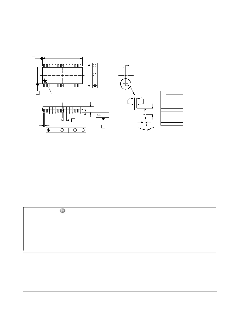
CS5305
http://onsemi.com
32
PACKAGE DIMENSIONS
A1
1
15
14
28
B
S
A
M
0.025
B
S
C
M
0.25
B
M
SEATING
PLANE
A
NOTES:
1. DIMENSIONS ARE IN MILLIMETERS.
2. INTERPRET DIMENSIONS AND TOLERANCES
PER ASME Y14.5M, 1994.
3. DIMENSIONS D AND E DO NOT INCLUDE MOLD
PROTRUSIONS.
4. MAXIMUM MOLD PROTRUSION 0.015 PER SIDE.
5. DIMENSION B DOES NOT INCLUDE DAMBAR
PROTRUSION. ALLOWABLE DAMBAR
PROTRUSION SHALL BE 0.13 TOTAL IN EXCESS
OF B DIMENSION AT MAXIMUM MATERIAL
CONDITION.
DIM
MIN
MAX
MILLIMETERS
A
2.35
2.65
A1
0.13
0.29
B
0.35
0.49
C
0.23
0.32
D
17.80
18.05
E
7.40
7.60
e
1.27 BSC
H
10.05
10.55
L
0.41
0.90
q
0
8
_
_
L
q
C
PIN 1 IDENT
A
B
D
E
H
e
0.10
C
SO≠28L
DW SUFFIX
CASE 751F≠05
ISSUE F
ON Semiconductor and are trademarks of Semiconductor Components Industries, LLC (SCILLC). SCILLC reserves the right to make changes
without further notice to any products herein. SCILLC makes no warranty, representation or guarantee regarding the suitability of its products for any particular
purpose, nor does SCILLC assume any liability arising out of the application or use of any product or circuit, and specifically disclaims any and all liability,
including without limitation special, consequential or incidental damages. "Typical" parameters which may be provided in SCILLC data sheets and/or
specifications can and do vary in different applications and actual performance may vary over time. All operating parameters, including "Typicals" must be
validated for each customer application by customer's technical experts. SCILLC does not convey any license under its patent rights nor the rights of others.
SCILLC products are not designed, intended, or authorized for use as components in systems intended for surgical implant into the body, or other applications
intended to support or sustain life, or for any other application in which the failure of the SCILLC product could create a situation where personal injury or
death may occur. Should Buyer purchase or use SCILLC products for any such unintended or unauthorized application, Buyer shall indemnify and hold
SCILLC and its officers, employees, subsidiaries, affiliates, and distributors harmless against all claims, costs, damages, and expenses, and reasonable
attorney fees arising out of, directly or indirectly, any claim of personal injury or death associated with such unintended or unauthorized use, even if such claim
alleges that SCILLC was negligent regarding the design or manufacture of the part. SCILLC is an Equal Opportunity/Affirmative Action Employer.
PUBLICATION ORDERING INFORMATION
JAPAN: ON Semiconductor, Japan Customer Focus Center
4≠32≠1 Nishi≠Gotanda, Shinagawa≠ku, Tokyo, Japan 141≠0031
Phone: 81≠3≠5740≠2700
Email: r14525@onsemi.com
ON Semiconductor Website: http://onsemi.com
For additional information, please contact your local
Sales Representative.
CS5305/D
Patents Pending.
V
2
is a trademark of Switch Power, Inc.
Literature Fulfillment:
Literature Distribution Center for ON Semiconductor
P.O. Box 5163, Denver, Colorado 80217 USA
Phone: 303≠675≠2175 or 800≠344≠3860 Toll Free USA/Canada
Fax: 303≠675≠2176 or 800≠344≠3867 Toll Free USA/Canada
Email: ONlit@hibbertco.com
N. American Technical Support: 800≠282≠9855 Toll Free USA/Canada