 | ÐлекÑÑоннÑй компоненÑ: LM201ADR2 | СкаÑаÑÑ:  PDF PDF  ZIP ZIP |
LM301A
©
Semiconductor Components Industries, LLC, 2002
January, 2002 Rev. 7
1
Publication Order Number:
LM301A/D
LM301A, LM201A
Non Compensated Single
Operational Amplifiers
A general purpose operational amplifier that allows the user to
choose the compensation capacitor best suited to his needs. With
proper compensation, summing amplifier slew rates to 10 V/
µ
s can be
obtained.
·
Low Input Offset Current: 20 nA Maximum Over Temperature
Range
·
External Frequency Compensation for Flexibility
·
Class AB Output Provides Excellent Linearity
·
Output Short Circuit Protection
·
Guaranteed Drift Characteristics
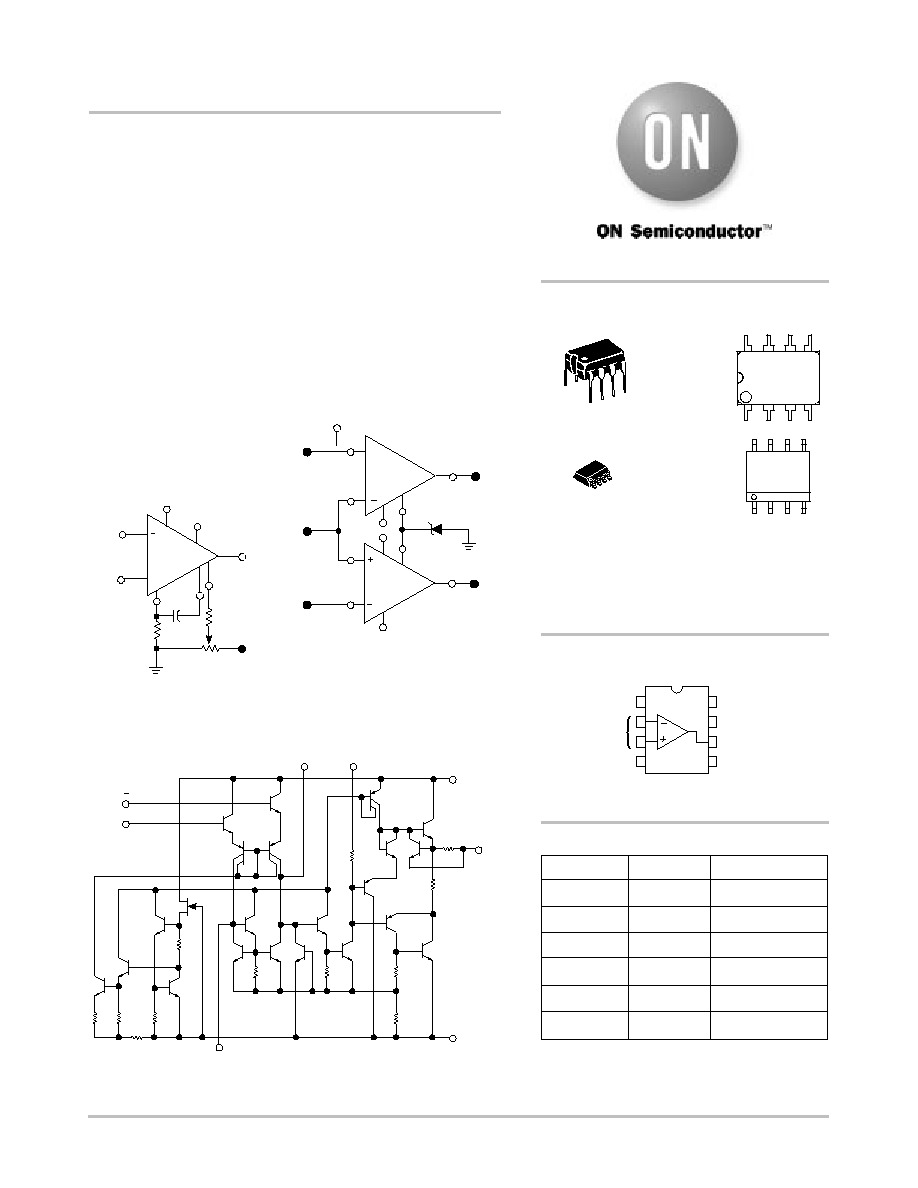
Figure 1. Standard
Compensation and
Offset Balancing Circuit
Balance
V
EE
V
CC
Output
Inverting
Input
Balance
10 M
Freq
Compen
30 pF
V
EE
20 k
+
Non-
Inverting
Input
5.1 M
V
CC
VO
V
UT
V
I
V
EE
V
CC
V
LT
V
EE
MZ4622 or Equiv.
VO
V
O
= 4.8 V for
V
LT
V
I
V
UT
V
O
= -0.4 V
V
I
< V
LT
or V
I
> V
UT
(Pins Not Shown Are Not Connected)
+
Inputs
Balance
Compensation
V
CC
Output
V
EE
Balance
25
500
50
80 k
1.0 k
40 k
40 k
10 k
20 k
5 k
450
250
3.9 V
+
Figure 2. DoubleEnded
Limit Detector
Figure 3. Representative Circuit Schematic
Device
Package
Shipping
ORDERING INFORMATION
LM301AD
SO8
98 Units/Rail
LM301AN
PDIP8
LM201AD
SO8
PDIP8
N SUFFIX
CASE 626
1
8
http://onsemi.com
50 Units/Rail
98 Units/Rail
SO8
D SUFFIX
CASE 751
1
8
Compensation
V
CC
Output
Balance
V
EE 4
Balance
1
2
3
8
7
6
5
Inputs
(Top View)
PIN CONNECTIONS
LM201ADR2
SO8
2500 Tape & Reel
LM301ADR2
SO8
2500 Tape & Reel
LM201AN
PDIP8
50 Units/Rail
MARKING
DIAGRAMS
x
= 2 or 3
A
= Assembly Location
WL, L
= Wafer Lot
YY, Y
= Year
WW, W
= Work Week
1
8
LMx01AN
AWL
YYWW
ALYWA
LMx01
1
8
LM301A, LM201A
http://onsemi.com
2
MAXIMUM RATINGS
Value
Rating
Symbol
LM201A
LM301A
Unit
Power Supply Voltage
V
CC,
V
EE
±
22
±
18
Vdc
Input Differential Voltage
V
ID
±
30
V
Input Common Mode Range (Note 1)
V
ICR
±
15
V
Output Short Circuit Duration
t
SC
Continuous
Power Dissipation (Package Limitation)
P
D
Plastic DualInLine Package
625
625
mW
Derate above T
A
= +25
°
C
5.0
5.0
mW/
°
C
Operating Ambient Temperature Range
T
A
25 to +85
0 to +70
°
C
Storage Temperature Range
T
stg
65 to +150
°
C
ELECTRICAL CHARACTERISTICS
(T
A
= +25
°
C, unless otherwise noted.) Unless otherwise specified, these specifications apply
for supply voltages from
±
5.0 V to
±
20 V for the LM201A, and from
±
5.0 V to
±
15 V for the LM301A.
LM201A
LM301A
Characteristic
Symbol
Min
Typ
Max
Min
Typ
Max
Unit
Input Offset Voltage (R
S
50 k
)
V
IO
0.7
2.0
2.0
7.5
mV
Input Offset Current
I
IO
1.5
10
3.0
50
nA
Input Bias Current
I
IB
30
75
70
250
nA
Input Resistance
r
i
1.5
4.0
0.5
2.0
M
Supply Current
I
CC
,I
EE
mA
V
CC
/V
EE
=
±
20 V
1.8
3.0
V
CC
/V
EE
=
±
15 V
1.8
3.0
Large Signal Voltage Gain
A
V
50
160
25
160
V/mV
(V
CC
/V
EE
=
±
15 V, V
O
=
±
10 V, R
L
> 2.0 k
)
The following specifications apply over the operating temperature range.
Input Offset Voltage (R
S
50 k
)
V
IO
3.0
10
mV
Input Offset Current
I
IO
20
70
nA
Avg Temperature Coefficient of Input Offset
Voltage (Note 2)
V
IO
/
T
3.0
15
6.0
30
µ
V/
°
C
T
A
(min)
T
A
T
A
(max)
Avg Temperature Coefficient of Input Offset
Current (Note 2)
I
IO
/
T
nA/
°
C
+25
°
C
T
A
T
A
(max)
0.01
0.1
0.01
0.3
T
A
(min)
T
A
25
°
C
0.02
0.2
0.02
0.6
Input Bias Current
I
IB
100
300
nA
Large Signal Voltage Gain
A
VOL
25
15
V/mV
(V
CC
/V
EE
=
±
15 V, V
O
=
±
10V, R
L
> 2.0 k
)
Input Voltage Range
V
ICR
V
V
CC
/V
EE
=
±
20 V
15
+15
V
CC
/V
EE
=
±
15 V
12
+12
Common Mode Rejection (R
S
50 k
)
CMR
80
96
70
90
dB
Supply Voltage Rejection (R
S
50 k
)
PSR
80
96
70
96
dB
Output Voltage Swing
V
O
±
12
±
14
±
12
±
14
V
(V
CC
/V
EE
=
±
15 V, R
L
=
±
10 k
,
R
L
> 2.0 k
)
±
10
±
13
±
10
±
13
Supply Currents (T
A
= T
A
(max), V
CC
/V
EE
=
±
20 V)
I
CC
,I
EE
1.2
2.5
mA
1. For supply voltages less than
±
15 V, the absolute maximum input voltage is equal to the supply voltage.
2. Guaranteed by design.
LM301A, LM201A
http://onsemi.com
3
C1 = 3.0 pF
C1 = 30 pF
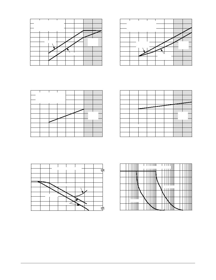
Single-Pole Compensation
Figure 4. Minimum Input Voltage Range
Figure 5. Minimum Output Voltage Swing
Figure 6. Minimum Voltage Gain
Figure 7. Typical Supply Currents
Figure 8. Open Loop Frequency Response
Figure 9. Large Signal Frequency Response
V IR
, INPUT
VOL
T
AGE RANGE (V)
V OR
, OUTPUT
VOL
T
AGE RANGE ( V)
±
A V
, VOL
T
AGE GAIN (dB)
A V
, VOL
T
AGE GAIN (dB)
CC
EE
, SUPPL
Y
CURRENTS (mA)
II
,
V
CC
, ( -V
EE
), SUPPLY VOLTAGE (V)
V
CC
, ( -V
EE
), SUPPLY VOLTAGE (V)
V
CC
, ( -V
EE
), SUPPLY VOLTAGE (V)
V
CC
, ( -V
EE
), SUPPLY VOLTAGE (V)
f, FREQUENCY (Hz)
f, FREQUENCY (Hz)
Phase
Gain
C1 = 3.0 pF
C1 = 30 pF
20
16
12
8.0
4.0
0
0
5.0
10
15
20
20
16
12
8.0
4.0
0
0
5.0
10
15
20
0
5.0
10
15
20
0
5.0
10
15
20
100
94
88
82
76
70
2.5
2.0
1.5
1.0
0.5
0
1.0 k
10 k
100 k
1.0 M
10 M
1.0
10
100
1.0 k
10 k
100 k 1.0 M 10 M
315
270
225
180
135
90
45
0
180
160
140
120
100
80
60
40
20
0
-20
15
10
5.0
0
Minimum
R
L
= 10 k
Minimum
R
L
= 2.0 k
T
A
= +25
°
C
Single-Pole Compensation
V OR
, OUTPUT
VOL
T
AGE RANGE ( V)
±
Negative
Positive
Applicable to the Specified
Operating Temperature
Ranges
Applicable to the Specified
Operating Temperature
Ranges
Applicable to the Specified
Operating Temperature
Ranges
LM201A
only
LM201A
only
LM201A
only
LM201A
only
LM301A, LM201A
http://onsemi.com
4
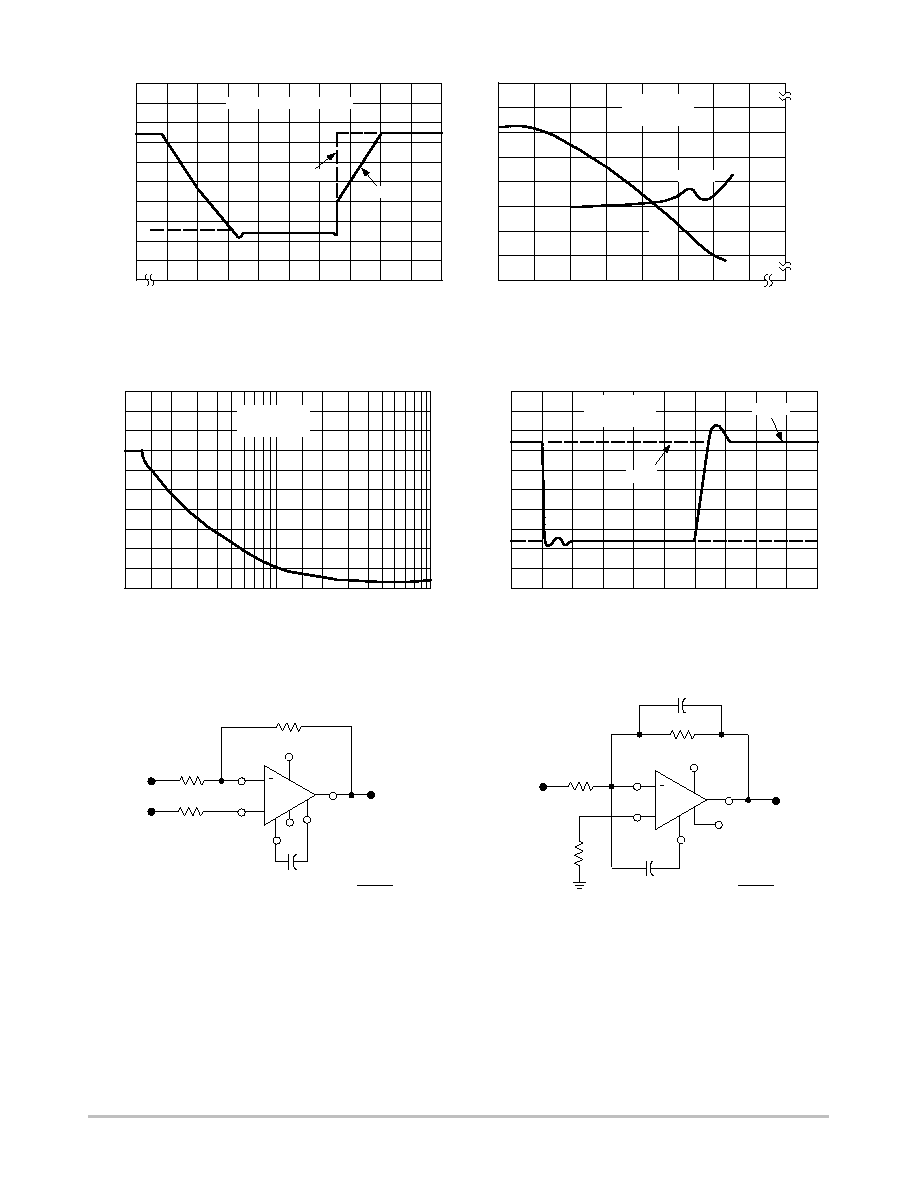
Figure 10. Voltage Follower Pulse Response
Figure 11. Open Loop Frequency Response
Figure 12. Large Signal Frequency Response
Figure 13. Inverter Pulse Response
Figure 14. SinglePole Compensation
Figure 15. Feedforward Compensation
t, TIME (
µ
s)
t, TIME (
µ
s)
f, FREQUENCY (Hz)
f, FREQUENCY (Hz)
V IR
, V
OR
VOL
T
AGE RANGE (
,
±
V)
A V
, VOL
T
AGE GAIN (dB)
PHASE LAG (DEGREES)
10
8.0
6.0
4.0
2.0
0
-2.0
-4.0
-6.0
-8.0
-10
0
10
20
30
40
50
60
70
80
90
140
120
100
80
60
40
20
0
-20
10
100 1.0 k
10 k 100 k
1.0 M 10 M 100 M
10
8.0
6.0
4.0
2.0
0
-2.0
-4.0
-6.0
-8.0
-10
0
1.0
2.0
3.0
4.0
5.0
6.0
7.0
8.0
9.0
1.0 M
10 M
100 k
0
18
16
12
8.0
4.0
225
180
135
90
45
0
Balance
1
4
V
EE
R2
R1
R3
2
3
7
6
8
C1
V
CC
VO
-VI
+V
I
Frequency
Compensation
C2
R2
R1
V
I
R3
C1
150 pF
Balance
V
EE
VO
2
3
6
7
4
1
C2 =
1
2
f
o
R2
f
o
= 3.0 MHz
+
+
C1
R1 C
s
R1 +R2
C
s
= 30 pF
V
CC
V OR
, OUTPUT
VOL
T
AGE RANGE ( V)
±
Single-Pole Compensation
Output
Input
V OR
, OUTPUT
VOL
T
AGE RANGE ( V)
±
Feedforward
Compensation
0
Output
Input
Feedforward
Compensation
Phase
Gain
Feedforward
Compensation
LM301A, LM201A
http://onsemi.com
5
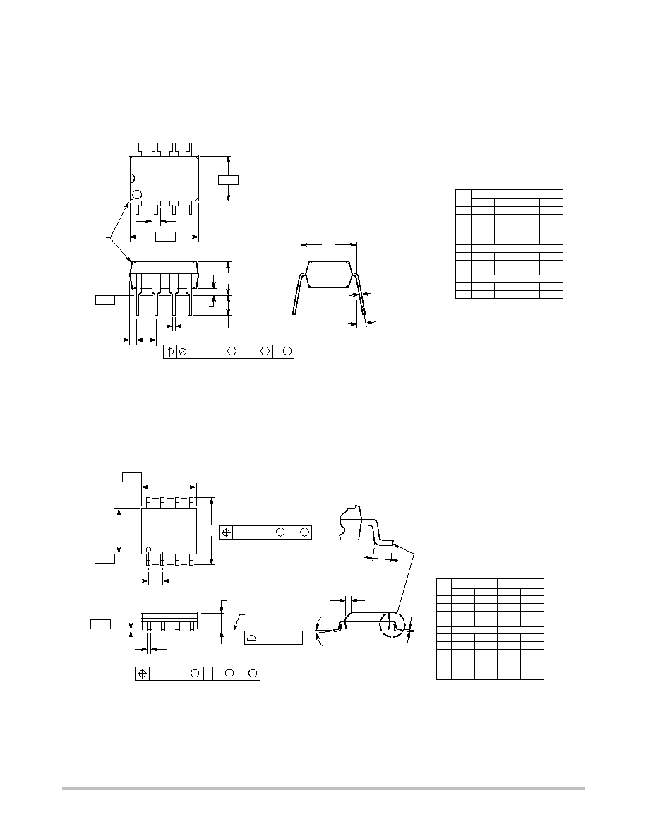
PACKAGE DIMENSIONS
PDIP8
N SUFFIX
CASE 62605
ISSUE L
NOTES:
1. DIMENSION L TO CENTER OF LEAD WHEN
FORMED PARALLEL.
2. PACKAGE CONTOUR OPTIONAL (ROUND OR
SQUARE CORNERS).
3. DIMENSIONING AND TOLERANCING PER ANSI
Y14.5M, 1982.
1
4
5
8
F
NOTE 2
A
B
T
SEATING
PLANE
H
J
G
D
K
N
C
L
M
M
A
M
0.13 (0.005)
B
M
T
DIM
MIN
MAX
MIN
MAX
INCHES
MILLIMETERS
A
9.40
10.16
0.370
0.400
B
6.10
6.60
0.240
0.260
C
3.94
4.45
0.155
0.175
D
0.38
0.51
0.015
0.020
F
1.02
1.78
0.040
0.070
G
2.54 BSC
0.100 BSC
H
0.76
1.27
0.030
0.050
J
0.20
0.30
0.008
0.012
K
2.92
3.43
0.115
0.135
L
7.62 BSC
0.300 BSC
M
---
10
---
10
N
0.76
1.01
0.030
0.040
_
_
SO8
D SUFFIX
CASE 75107
ISSUE W
SEATING
PLANE
1
4
5
8
N
J
X 45
_
K
NOTES:
1. DIMENSIONING AND TOLERANCING PER ANSI
Y14.5M, 1982.
2. CONTROLLING DIMENSION: MILLIMETER.
3. DIMENSION A AND B DO NOT INCLUDE MOLD
PROTRUSION.
4. MAXIMUM MOLD PROTRUSION 0.15 (0.006) PER
SIDE.
5. DIMENSION D DOES NOT INCLUDE DAMBAR
PROTRUSION. ALLOWABLE DAMBAR
PROTRUSION SHALL BE 0.127 (0.005) TOTAL IN
EXCESS OF THE D DIMENSION AT MAXIMUM
MATERIAL CONDITION.
A
B
S
D
H
C
0.10 (0.004)
DIM
A
MIN
MAX
MIN
MAX
INCHES
4.80
5.00
0.189
0.197
MILLIMETERS
B
3.80
4.00
0.150
0.157
C
1.35
1.75
0.053
0.069
D
0.33
0.51
0.013
0.020
G
1.27 BSC
0.050 BSC
H
0.10
0.25
0.004
0.010
J
0.19
0.25
0.007
0.010
K
0.40
1.27
0.016
0.050
M
0
8
0
8
N
0.25
0.50
0.010
0.020
S
5.80
6.20
0.228
0.244
X
Y
G
M
Y
M
0.25 (0.010)
Z
Y
M
0.25 (0.010)
Z
S
X
S
M
_
_
_
_