 | –≠–ª–µ–∫—Ç—Ä–æ–Ω–Ω—ã–π –∫–æ–º–ø–æ–Ω–µ–Ω—Ç: LM324N | –°–∫–∞—á–∞—Ç—å:  PDF PDF  ZIP ZIP |
©
Semiconductor Components Industries, LLC, 2002
May, 2002 ≠ Rev. 8
1
Publication Order Number:
LM324/D
LM324, LM324A, LM224,
LM2902, LM2902V, NCV2902
Single Supply Quad
Operational Amplifiers
The LM324 series are low≠cost, quad operational amplifiers with
true differential inputs. They have several distinct advantages over
standard operational amplifier types in single supply applications. The
quad amplifier can operate at supply voltages as low as 3.0 V or as
high as 32 V with quiescent currents about one≠fifth of those
associated with the MC1741 (on a per amplifier basis). The common
mode input range includes the negative supply, thereby eliminating the
necessity for external biasing components in many applications. The
output voltage range also includes the negative power supply voltage.
∑
Short Circuited Protected Outputs
∑
True Differential Input Stage
∑
Single Supply Operation: 3.0 V to 32 V (LM224, LM324, LM324A)
∑
Low Input Bias Currents: 100 nA Maximum (LM324A)
∑
Four Amplifiers Per Package
∑
Internally Compensated
∑
Common Mode Range Extends to Negative Supply
∑
Industry Standard Pinouts
∑
ESD Clamps on the Inputs Increase Ruggedness without Affecting
Device Operation
MAXIMUM RATINGS
(T
A
= +25
∞
C, unless otherwise noted.)
Rating
Symbol
LM224
LM324,
LM324A
LM2902,
LM2902V
Unit
Power Supply Voltages
Vdc
Single Supply
V
CC
32
26
Split Supplies
V
CC
, V
EE
±
16
±
13
Input Differential Voltage
Range (Note 1)
V
IDR
±
32
±
26
Vdc
Input Common Mode
Voltage Range
V
ICR
≠0.3 to 32
≠0.3 to 26
Vdc
Output Short Circuit
Duration
t
SC
Continuous
Junction Temperature
T
J
150
∞
C
Storage Temperature
Range
T
stg
≠65 to +150
∞
C
Operating Ambient
Temperature Range
T
A
∞
C
LM224
≠25 to +85
LM324, 324A
0 to +70
LM2902
≠40 to +105
LM2902V, NCV2902
≠40 to +125
1. Split Power Supplies.
PDIP≠14
N SUFFIX
CASE 646
1
14
SO≠14
D SUFFIX
CASE 751A
1
14
PIN CONNECTIONS
8
Out 4
Inputs 4
V
EE
, Gnd
Inputs 3
Out 3
9
10
11
12
13
14
2
Out 1
V
CC
Out 2
1
3
4
5
6
7
*
)
Inputs 1
Inputs 2
(Top View)
4
2
3
1
)
*
*
)
)
*
See general marking information in the device marking
section on page 10 of this data sheet.
DEVICE MARKING INFORMATION
See detailed ordering and shipping information in the package
dimensions section on page 9 of this data sheet.
ORDERING INFORMATION
1
14
TSSOP≠14
DTB SUFFIX
CASE 948G
http://onsemi.com
LM324, LM324A, LM224, LM2902, LM2902V, NCV2902
http://onsemi.com
2
ELECTRICAL CHARACTERISTICS
(V
CC
= 5.0 V, V
EE
= Gnd, T
A
= 25
∞
C, unless otherwise noted.)
LM224
LM324A
LM324
LM2902
LM2902V/NCV2902
Characteristics
Symbol
Min
Typ
Max
Min
Typ
Max
Min
Typ
Max
Min
Typ
Max
Min
Typ
Max
Unit
Input Offset Voltage
V
IO
mV
V
CC
= 5.0 V to 30 V
(26 V for LM2902, V),
V
ICR
= 0 V to
V
CC
≠1.7 V,
V
O
= 1.4 V, R
S
= 0
T
A
= 25
∞
C
≠
2.0
5.0
≠
2.0
3.0
≠
2.0
7.0
≠
2.0
7.0
≠
2.0
7.0
T
A
= T
high
(Note 2)
≠
≠
7.0
≠
≠
5.0
≠
≠
9.0
≠
≠
10
≠
≠
13
T
A
= T
low
(Note 2)
≠
≠
7.0
≠
≠
5.0
≠
≠
9.0
≠
≠
10
≠
≠
10
Average Temperature
Coefficient of Input
Offset Voltage
V
IO
/
T
≠
7.0
≠
≠
7.0
30
≠
7.0
≠
≠
7.0
≠
≠
7.0
≠
µ
V/
∞
C
T
A
= T
high
to T
low
(Notes 2 and 4)
Input Offset Current
I
IO
≠
3.0
30
≠
5.0
30
≠
5.0
50
≠
5.0
50
≠
5.0
50
nA
T
A
= T
high
to T
low
(Note 2)
≠
≠
100
≠
≠
75
≠
≠
150
≠
≠
200
≠
≠
200
Average Temperature
Coefficient of Input
Offset Current
I
IO
/
T
≠
10
≠
≠
10
300
≠
10
≠
≠
10
≠
≠
10
≠
pA/
∞
C
T
A
= T
high
to T
low
(Notes 2 and 4)
Input Bias Current
I
IB
≠
≠90
≠150
≠
≠45
≠100
≠
≠90
≠250
≠
≠90
≠250
≠
≠90
≠250
nA
T
A
= T
high
to T
low
(Note 2)
≠
≠
≠300
≠
≠
≠200
≠
≠
≠500
≠
≠
≠500
≠
≠
≠500
Input Common Mode
Voltage Range
(Note 3)
V
ICR
V
V
CC
= 30 V
(26 V for LM2902, V)
T
A
= +25
∞
C
0
≠
28.3
0
≠
28.3
0
≠
28.3
0
≠
24.3
0
≠
24.3
T
A
= T
high
to T
low
(Note 2)
0
≠
28
0
≠
28
0
≠
28
0
≠
24
0
≠
24
Differential Input
Voltage Range
V
IDR
≠
≠
V
CC
≠
≠
V
CC
≠
≠
V
CC
≠
≠
V
CC
≠
≠
V
CC
V
Large Signal Open
Loop Voltage Gain
A
VOL
V/mV
R
L
= 2.0 k
,
V
CC
= 15 V,
for Large V
O
Swing
50
100
≠
25
100
≠
25
100
≠
25
100
≠
25
100
≠
T
A
= T
high
to T
low
(Note 2)
25
≠
≠
15
≠
≠
15
≠
≠
15
≠
≠
15
≠
≠
Channel Separation
10 kHz
f
20 kHz,
Input Referenced
CS
≠
≠120
≠
≠
≠120
≠
≠
≠120
≠
≠
≠120
≠
≠
≠120
≠
dB
Common Mode
Rejection,
R
S
10 k
CMR
70
85
≠
65
70
≠
65
70
≠
50
70
≠
50
70
≠
dB
Power Supply
Rejection
PSR
65
100
≠
65
100
≠
65
100
≠
50
100
≠
50
100
≠
dB
2. LM224: T
low
= ≠25
∞
C, T
high
= +85
∞
C
LM324/LM324A: T
low
= 0
∞
C, T
high
= +70
∞
C
LM2902: T
low
= ≠40
∞
C, T
high
= +105
∞
C
LM2902V & NCV2902: T
low
= ≠40
∞
C, T
high
= +125
∞
C
NCV2902 is qualified for automotive use.
3. The input common mode voltage or either input signal voltage should not be allowed to go negative by more than 0.3 V. The upper end of
the common mode voltage range is V
CC
≠1.7 V.
4. Guaranteed by design.
LM324, LM324A, LM224, LM2902, LM2902V, NCV2902
http://onsemi.com
3
ELECTRICAL CHARACTERISTICS
(V
CC
= 5.0 V, V
EE
= Gnd, T
A
= 25
∞
C, unless otherwise noted.)
LM224
LM324A
LM324
LM2902
LM2902V/NCV2902
Characteristics
Symbol
Min
Typ
Max
Min
Typ
Max
Min
Typ
Max
Min
Typ
Max
Min
Typ
Max
Unit
Output Voltage≠
High Limit
(T
A
= T
high to
T
low
)
(Note 5)
V
OH
V
V
CC
= 5.0 V, R
L
=
2.0 k
, T
A
= 25
∞
C
3.3
3.5
≠
3.3
3.5
≠
3.3
3.5
≠
3.3
3.5
≠
3.3
3.5
≠
V
CC
= 30 V
(26 V for LM2902, V),
R
L
= 2.0 k
26
≠
≠
26
≠
≠
26
≠
≠
22
≠
≠
22
≠
≠
V
CC
= 30 V
(26 V for LM2902, V),
R
L
= 10 k
27
28
≠
27
28
≠
27
28
≠
23
24
≠
23
24
≠
Output Voltage ≠
Low Limit,
V
CC
= 5.0 V,
R
L
= 10 k
,
T
A
= T
high
to T
low
(Note 5)
V
OL
≠
5.0
20
≠
5.0
20
≠
5.0
20
≠
5.0
100
≠
5.0
100
mV
Output Source Current
(V
ID
= +1.0 V,
V
CC
= 15 V)
I
O +
mA
T
A
= 25
∞
C
20
40
≠
20
40
≠
20
40
≠
20
40
≠
20
40
≠
T
A
= T
high
to T
low
(Note 5)
10
20
≠
10
20
≠
10
20
≠
10
20
≠
10
20
≠
Output Sink Current
I
O ≠
mA
(V
ID
= ≠1.0 V,
V
CC
= 15 V)
T
A
= 25
∞
C
10
20
≠
10
20
≠
10
20
≠
10
20
≠
10
20
≠
T
A
= T
high
to T
low
(Note 5)
5.0
8.0
≠
5.0
8.0
≠
5.0
8.0
≠
5.0
8.0
≠
5.0
8.0
≠
(V
ID
= ≠1.0 V,
V
O
= 200 mV,
T
A
= 25
∞
C)
12
50
≠
12
50
≠
12
50
≠
≠
≠
≠
≠
≠
≠
µ
A
Output Short Circuit
to Ground
(Note 6)
I
SC
≠
40
60
≠
40
60
≠
40
60
≠
40
60
≠
40
60
mA
Power Supply Current
(T
A
= T
high
to T
low
)
(Note 5)
I
CC
mA
V
CC
= 30 V
(26 V for LM2902, V),
V
O
= 0 V, R
L
=
≠
≠
3.0
≠
1.4
3.0
≠
≠
3.0
≠
≠
3.0
≠
≠
3.0
V
CC
= 5.0 V,
V
O
= 0 V, R
L
=
≠
≠
1.2
≠
0.7
1.2
≠
≠
1.2
≠
≠
1.2
≠
≠
1.2
5. LM224: T
low
= ≠25
∞
C, T
high
= +85
∞
C
LM324/LM324A: T
low
= 0
∞
C, T
high
= +70
∞
C
LM2902: T
low
= ≠40
∞
C, T
high
= +105
∞
C
LM2902V & NCV2902: T
low
= ≠40
∞
C, T
high
= +125
∞
C
NCV2902 is qualified for automotive use.
6. The input common mode voltage or either input signal voltage should not be allowed to go negative by more than 0.3 V. The upper end of
the common mode voltage range is V
CC
≠1.7 V.
LM324, LM324A, LM224, LM2902, LM2902V, NCV2902
http://onsemi.com
4
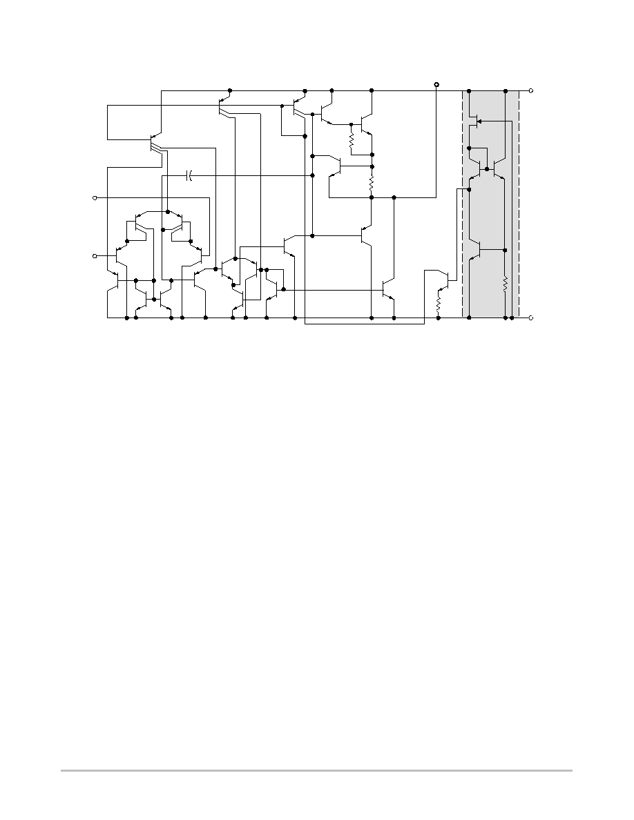
Figure 1. Representative Circuit Diagram
(One≠Fourth of Circuit Shown)
Output
Bias Circuitry
Common to Four
Amplifiers
V
CC
V
EE
/Gnd
Inputs
Q2
Q3
Q4
Q5
Q26
Q7
Q8
Q6
Q9
Q11
Q10
Q1
2.4 k
Q25
Q22
40 k
Q13
Q14
Q15
Q16
Q19
5.0 pF
Q18
Q17
Q20
Q21
2.0 k
Q24
Q23
Q12
25
+
-
LM324, LM324A, LM224, LM2902, LM2902V, NCV2902
http://onsemi.com
5
CIRCUIT DESCRIPTION
The LM324 series is made using four internally
compensated, two≠stage operational amplifiers. The first
stage of each consists of differential input devices Q20 and
Q18 with input buffer transistors Q21 and Q17 and the
differential to single ended converter Q3 and Q4. The first
stage performs not only the first stage gain function but also
performs the level shifting and transconductance reduction
functions. By reducing the transconductance, a smaller
compensation capacitor (only 5.0 pF) can be employed, thus
saving chip area. The transconductance reduction is
accomplished by splitting the collectors of Q20 and Q18.
Another feature of this input stage is that the input common
mode range can include the negative supply or ground, in
single supply operation, without saturating either the input
devices or the differential to single≠ended converter. The
second stage consists of a standard current source load
amplifier stage.
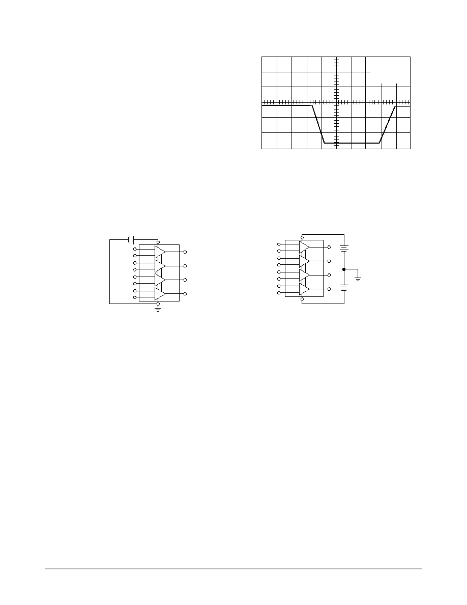
Figure 2. Large Signal Voltage Follower Response
V
CC
= 15 Vdc
R
L
= 2.0 k
T
A
= 25
∞
C
5.0
µ
s/DIV
1.0 V/DIV
Each amplifier is biased from an internal≠voltage
regulator which has a low temperature coefficient thus
giving each amplifier good temperature characteristics as
well as excellent power supply rejection.
Single Supply
Split Supplies
V
CC
V
EE
/Gnd
3.0 V to V
CC(max)
1
2
3
4
V
CC
1
2
3
4
V
EE
1.5 V to V
CC(max)
1.5 V to V
EE(max)
Figure 3.
LM324, LM324A, LM224, LM2902, LM2902V, NCV2902
http://onsemi.com
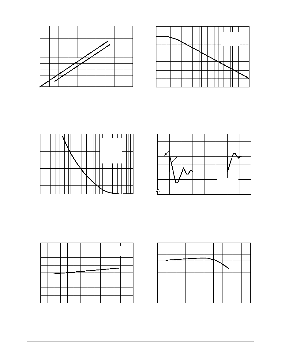
6
V OR
, OUTPUT
VOL
T
AGE RANGE (V
)
pp
V O
, OUTPUT
VOL
T
AGE (mV)
14
12
10
8.0
6.0
4.0
2.0
0
1.0
10
100
1000
f, FREQUENCY (kHz)
550
500
450
400
350
300
250
200
0
0
1.0
2.0
3.0
4.0
5.0
6.0
7.0
8.0
t, TIME (
µ
s)
2.4
2.1
1.8
1.5
1.2
0.9
0.6
0.3
0
0
5.0
10
15
20
25
30
35
V
CC
, POWER SUPPLY VOLTAGE (V)
V
CC
, POWER SUPPLY VOLTAGE (V)
90
80
70
0
2.0
4.0
6.0
8.0
10
12
14
16
18
20
I , POWER SUPPL
Y
CURRENT
(mA)
CC
I , INPUT
BIAS CURRENT
(nA)
IB
V
CC
= 30 V
V
EE
= Gnd
T
A
= 25
∞
C
C
L
= 50 pF
Input
Output
V , INPUT
VOL
T
AGE (V)
I
18
16
14
12
10
8.0
6.0
4.0
2.0
0
20
0
2.0 4.0 6.0 8.0
10
12
14 16
18
20
±
V
CC
/V
EE,
POWER SUPPLY VOLTAGES (V)
±
Positive
Negative
T
A
= 25
∞
C
R
L
=
R
R
L
= 2.0 k
V
CC
= 15 V
V
EE
= Gnd
Gain = -100
R
I
= 1.0 k
R
F
= 100 k
Figure 4. Input Voltage Range
Figure 5. Open Loop Frequency
120
100
80
60
40
20
0
-20
1.0
10
100
1.0 k
10 k
100 k
1.0 M
f, FREQUENCY (Hz)
A
, LARGE-SIGNAL VOL
OPEN LOOP
VOL
T
AGE GAIN (dB)
V
CC
= 15 V
V
EE
= Gnd
T
A
= 25
∞
C
Figure 6. Large≠Signal Frequency Response
Figure 7. Small≠Signal Voltage Follower
Pulse Response (Noninverting)
Figure 8. Power Supply Current versus
Power Supply Voltage
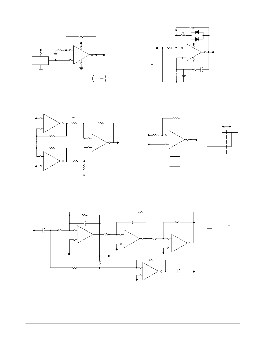
Figure 9. Input Bias Current versus
Power Supply Voltage
LM324, LM324A, LM224, LM2902, LM2902V, NCV2902
http://onsemi.com
7
2
1
R1
T
BP
R1 + R2
R1
R1 + R2
e
o
e
1
e
2
e
o
= C (1 + a + b) (e
2
- e
1
)
R1
a R1
b R1
R
-
+
+
-
-
+
R
+
-
R1
R2
V
O
V
ref
V
in
V
OH
V
O
V
OL
V
inL
=
R1
(V
OL
- V
ref
) + V
ref
V
inH
=
(V
OH
- V
ref
) + V
ref
H = R1 + R2 (V
OH
- V
OL
)
R1
-
+
-
+
-
+
R
C
R2
R1
R3
C1
100 k
R
C
R
C1
R2
100 k
V
in
V
ref
V
ref
V
ref
Vref
Bandpass
Output
f
o
= 2
RC
R1 = QR
R2 =
R3 = T
N R2
C1 = 10C
1
Notch Output
V
ref
=
V
CC
Hysteresis
1
C R
V
inL
V
inH
V
ref
Where: T
BP
= Center Frequency Gain
Where:
T
N
= Passband Notch Gain
R = 160 k
C = 0.001
µ
F
R1 = 1.6 M
R2 = 1.6 M
R3 = 1.6 M
For: f
o
= 1.0 kHz
For:
Q = 10
For:
T
BP
= 1
For:
T
N
= 1
-
+
MC1403
1/4
LM324
-
+
R1
V
CC
V
CC
V
O
2.5 V
R2
50 k
10 k
V
ref
V
ref
= V
CC
2
5.0 k
R
C
R
C
+
-
V
O
2
RC
1
For: f
o
= 1.0 kHz
R = 16 k
C = 0.01
µ
F
V
O
= 2.5 V 1 + R1
R2
1
V
CC
f
o
=
1/4
LM324
1/4
LM324
1/4
LM324
1/4
LM324
1
C R
1/4
LM324
1/4
LM324
1/4
LM324
1/4
LM324
1/4
LM324
Figure 10. Voltage Reference
Figure 11. Wien Bridge Oscillator
Figure 12. High Impedance Differential Amplifier
Figure 13. Comparator with Hysteresis
Figure 14. Bi≠Quad Filter
LM324, LM324A, LM224, LM2902, LM2902V, NCV2902
http://onsemi.com
8
2
1
For less than 10% error from operational amplifier,
If source impedance varies, filter may be preceded with
voltage follower buffer to stabilize filter parameters.
where f
o
and BW are expressed in Hz.
Q
o
f
o
BW
< 0.1
Given: f
o
= center frequency
A(f
o
) = gain at center frequency
Choose value f
o
, C
Then:
R3 =
Q
f
o
C
R3
R1 = 2 A(f
o
)
R1 R3
4Q
2
R1 - R3
R2 =
+
-
+
-
V
ref
=
V
CC
V
ref
f =
R1 + R
C
4 CR
f
R1
R3 =
R2 R1
R2 + R1
R2
300 k
75 k
R3
R1
100 k
C
Triangle Wave
Output
Square
Wave
Output
V
in
R
f
if
V
ref
1/4
LM324
1/4
LM324
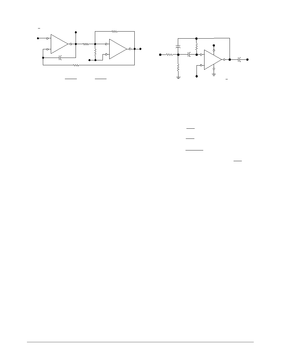
Figure 15. Function Generator
Figure 16. Multiple Feedback Bandpass Filter
V
ref
= V
CC
1
2
-
+
V
CC
R3
R1
R2
V
ref
C
C
V
O
CO = 10 C
C
O
1/4
LM324
LM324, LM324A, LM224, LM2902, LM2902V, NCV2902
http://onsemi.com
9
ORDERING INFORMATION
Device
Package
Operating Temperature Range
Shipping
LM224D
SO≠14
55 Units/Rail
LM224DR2
SO≠14
2500 Tape & Reel
LM224DTB
TSSOP≠14
≠25
∞
to +85
∞
C
96 Units/Rail
LM224DTBR2
TSSOP≠14
5 o 85 C
2500 Tape & Reel
LM224N
PDIP≠14
25 Units/Rail
LM324D
SO≠14
55 Units/Rail
LM324DR2
SO≠14
2500 Tape & Reel
LM324DTB
TSSOP≠14
96 Units/Rail
LM324DTBR2
TSSOP≠14
2500 Tape & Reel
LM324N
PDIP≠14
0
∞
to +70
∞
C
25 Units/Rail
LM324AD
SO≠14
0
∞
to +70
∞
C
55 Units/Rail
LM324ADR2
SO≠14
2500 Tape & Reel
LM324ADTB
TSSOP≠14
96 Units/Rail
LM324ADTBR2
TSSOP≠14
2500 Tape & Reel
LM324AN
PDIP≠14
25 Units/Rail
LM2902D
SO≠14
55 Units/Rail
LM2902DR2
SO≠14
2500 Tape & Reel
LM2902DTB
TSSOP≠14
≠40
∞
to +105
∞
C
96 Units/Rail
LM2902DTBR2
TSSOP≠14
0 o
05 C
2500 Tape & Reel
LM2902N
PDIP≠14
25 Units/Rail
LM2902VD
SO≠14
55 Units/Rail
LM2902VDR2
SO≠14
2500 Tape & Reel
LM2902VDTB
TSSOP≠14
40
∞
to +125
∞
C
96 Units/Rail
LM2902VDTBR2
TSSOP≠14
≠40
∞
to +125
∞
C
2500 Tape & Reel
LM2902VN
PDIP≠14
25 Units/Rail
NCV2902DR2
SO≠14
2500 Tape & Reel
LM324, LM324A, LM224, LM2902, LM2902V, NCV2902
http://onsemi.com
10
MARKING DIAGRAMS
x
= 2 or 3
A
= Assembly Location
WL
= Wafer Lot
YY, Y
= Year
WW, W = Work Week
PDIP≠14
N SUFFIX
CASE 646
SO≠14
D SUFFIX
CASE 751A
1
14
LM324AN
AWLYYWW
1
14
LMx24N
AWLYYWW
1
14
LM2902N
AWLYYWW
1
14
LM2902VN
AWLYYWW
1
14
LM324AD
AWLYWW
1
14
LMx24D
AWLYWW
1
14
LM2902D
AWLYWW
1
14
LM2902VD
AWLYWW
*This marking diagram also applies to NCV2902.
TSSOP≠14
DTB SUFFIX
CASE 948G
1
14
x24
AWYW
1
14
324A
AWYW
1
14
2902
AWYW
1
14
2902
V
AWYW
*
LM324, LM324A, LM224, LM2902, LM2902V, NCV2902
http://onsemi.com
11
PACKAGE DIMENSIONS
PDIP≠14
N SUFFIX
CASE 646≠06
ISSUE M
1
7
14
8
B
A
DIM
MIN
MAX
MIN
MAX
MILLIMETERS
INCHES
A
0.715
0.770
18.16
18.80
B
0.240
0.260
6.10
6.60
C
0.145
0.185
3.69
4.69
D
0.015
0.021
0.38
0.53
F
0.040
0.070
1.02
1.78
G
0.100 BSC
2.54 BSC
H
0.052
0.095
1.32
2.41
J
0.008
0.015
0.20
0.38
K
0.115
0.135
2.92
3.43
L
M
---
10 ---
10
N
0.015
0.039
0.38
1.01
_
_
NOTES:
1. DIMENSIONING AND TOLERANCING PER ANSI
Y14.5M, 1982.
2. CONTROLLING DIMENSION: INCH.
3. DIMENSION L TO CENTER OF LEADS WHEN
FORMED PARALLEL.
4. DIMENSION B DOES NOT INCLUDE MOLD FLASH.
5. ROUNDED CORNERS OPTIONAL.
F
H
G
D
K
C
SEATING
PLANE
N
≠T≠
14 PL
M
0.13 (0.005)
L
M
J
0.290
0.310
7.37
7.87
SO≠14
D SUFFIX
CASE 751A≠03
ISSUE F
NOTES:
1. DIMENSIONING AND TOLERANCING PER ANSI
Y14.5M, 1982.
2. CONTROLLING DIMENSION: MILLIMETER.
3. DIMENSIONS A AND B DO NOT INCLUDE
MOLD PROTRUSION.
4. MAXIMUM MOLD PROTRUSION 0.15 (0.006)
PER SIDE.
5. DIMENSION D DOES NOT INCLUDE DAMBAR
PROTRUSION. ALLOWABLE DAMBAR
PROTRUSION SHALL BE 0.127 (0.005) TOTAL
IN EXCESS OF THE D DIMENSION AT
MAXIMUM MATERIAL CONDITION.
≠A≠
≠B≠
G
P
7 PL
14
8
7
1
M
0.25 (0.010)
B
M
S
B
M
0.25 (0.010)
A
S
T
≠T≠
F
R
X 45
SEATING
PLANE
D
14 PL
K
C
J
M
_
DIM
MIN
MAX
MIN
MAX
INCHES
MILLIMETERS
A
8.55
8.75
0.337
0.344
B
3.80
4.00
0.150
0.157
C
1.35
1.75
0.054
0.068
D
0.35
0.49
0.014
0.019
F
0.40
1.25
0.016
0.049
G
1.27 BSC
0.050 BSC
J
0.19
0.25
0.008
0.009
K
0.10
0.25
0.004
0.009
M
0
7
0
7
P
5.80
6.20
0.228
0.244
R
0.25
0.50
0.010
0.019
_
_
_
_
LM324, LM324A, LM224, LM2902, LM2902V, NCV2902
http://onsemi.com
12
PACKAGE DIMENSIONS
TSSOP≠14
DTB SUFFIX
CASE 948G≠01
ISSUE O
DIM
MIN
MAX
MIN
MAX
INCHES
MILLIMETERS
A
4.90
5.10
0.193
0.200
B
4.30
4.50
0.169
0.177
C
---
1.20
---
0.047
D
0.05
0.15
0.002
0.006
F
0.50
0.75
0.020
0.030
G
0.65 BSC
0.026 BSC
H
0.50
0.60
0.020
0.024
J
0.09
0.20
0.004
0.008
J1
0.09
0.16
0.004
0.006
K
0.19
0.30
0.007
0.012
K1
0.19
0.25
0.007
0.010
L
6.40 BSC
0.252 BSC
M
0
8
0
8
NOTES:
1. DIMENSIONING AND TOLERANCING PER ANSI
Y14.5M, 1982.
2. CONTROLLING DIMENSION: MILLIMETER.
3. DIMENSION A DOES NOT INCLUDE MOLD FLASH,
PROTRUSIONS OR GATE BURRS. MOLD FLASH
OR GATE BURRS SHALL NOT EXCEED 0.15
(0.006) PER SIDE.
4. DIMENSION B DOES NOT INCLUDE INTERLEAD
FLASH OR PROTRUSION. INTERLEAD FLASH OR
PROTRUSION SHALL NOT EXCEED
0.25 (0.010) PER SIDE.
5. DIMENSION K DOES NOT INCLUDE DAMBAR
PROTRUSION. ALLOWABLE DAMBAR
PROTRUSION SHALL BE 0.08 (0.003) TOTAL IN
EXCESS OF THE K DIMENSION AT MAXIMUM
MATERIAL CONDITION.
6. TERMINAL NUMBERS ARE SHOWN FOR
REFERENCE ONLY.
7. DIMENSION A AND B ARE TO BE DETERMINED
AT DATUM PLANE -W-.
_
_
_
_
S
U
0.15 (0.006) T
2X
L/2
S
U
M
0.10 (0.004)
V
S
T
L
≠U≠
SEATING
PLANE
0.10 (0.004)
≠T≠
«««
«««
SECTION N≠N
DETAIL E
J J1
K
K1
……
……
DETAIL E
F
M
≠W≠
0.25 (0.010)
8
14
7
1
PIN 1
IDENT.
H
G
A
D
C
B
S
U
0.15 (0.006) T
≠V≠
14X REF
K
N
N
ON Semiconductor and are registered trademarks of Semiconductor Components Industries, LLC (SCILLC). SCILLC reserves the right to make
changes without further notice to any products herein. SCILLC makes no warranty, representation or guarantee regarding the suitability of its products for any
particular purpose, nor does SCILLC assume any liability arising out of the application or use of any product or circuit, and specifically disclaims any and all
liability, including without limitation special, consequential or incidental damages. "Typical" parameters which may be provided in SCILLC data sheets and/or
specifications can and do vary in different applications and actual performance may vary over time. All operating parameters, including "Typicals" must be
validated for each customer application by customer's technical experts. SCILLC does not convey any license under its patent rights nor the rights of others.
SCILLC products are not designed, intended, or authorized for use as components in systems intended for surgical implant into the body, or other applications
intended to support or sustain life, or for any other application in which the failure of the SCILLC product could create a situation where personal injury or death
may occur. Should Buyer purchase or use SCILLC products for any such unintended or unauthorized application, Buyer shall indemnify and hold SCILLC
and its officers, employees, subsidiaries, affiliates, and distributors harmless against all claims, costs, damages, and expenses, and reasonable attorney fees
arising out of, directly or indirectly, any claim of personal injury or death associated with such unintended or unauthorized use, even if such claim alleges that
SCILLC was negligent regarding the design or manufacture of the part. SCILLC is an Equal Opportunity/Affirmative Action Employer.
PUBLICATION ORDERING INFORMATION
JAPAN: ON Semiconductor, Japan Customer Focus Center
4≠32≠1 Nishi≠Gotanda, Shinagawa≠ku, Tokyo, Japan 141≠0031
Phone: 81≠3≠5740≠2700
Email: r14525@onsemi.com
ON Semiconductor Website: http://onsemi.com
For additional information, please contact your local
Sales Representative.
LM324/D
Literature Fulfillment:
Literature Distribution Center for ON Semiconductor
P.O. Box 5163, Denver, Colorado 80217 USA
Phone: 303≠675≠2175 or 800≠344≠3860 Toll Free USA/Canada
Fax: 303≠675≠2176 or 800≠344≠3867 Toll Free USA/Canada
Email: ONlit@hibbertco.com
N. American Technical Support: 800≠282≠9855 Toll Free USA/Canada