
This document,
MC74HC4051/D
has been canceled and
replaced by
MC74HC4051A/D
LAN was sent 9/28/01
http://onsemi.com
MC54/74HC4051 MC74HC4052 MC54/74HC4053
Analog Multiplexers/
Demultiplexers
High≠Performance Silicon≠Gate CMOS
The MC54/74HC4051, MC74HC4052 and MC54/74HC4053 utilize sili-
con≠gate CMOS technology to achieve fast propagation delays, low ON
resistances, and low OFF leakage currents. These analog multiplexers/
demultiplexers control analog voltages that may vary across the complete
power supply range (from V
CC
to V
EE
).
The HC4051, HC4052 and HC4053 are identical in pinout to the
metal≠gate MC14051B, MC14052B and MC14053B. The Channel≠Select
inputs determine which one of the Analog Inputs/Outputs is to be connected,
by means of an analog switch, to the Common Output/Input. When the
Enable pin is HIGH, all analog switches are turned off.
The Channel≠Select and Enable inputs are compatible with standard
CMOS outputs; with pullup resistors they are compatible with LSTTL
outputs.
These devices have been designed so that the ON resistance (R
on
) is
more linear over input voltage than R
on
of metal≠gate CMOS analog
switches.
For multiplexers/demultiplexers with channel≠select latches, see
HC4351, HC4352 and HC4353.
∑
Fast Switching and Propagation Speeds
∑
Low Crosstalk Between Switches
∑
Diode Protection on All Inputs/Outputs
∑
Analog Power Supply Range (V
CC
≠ V
EE
) = 2.0 to 12.0 V
∑
Digital (Control) Power Supply Range (V
CC
≠ GND) = 2.0 to 6.0 V
∑
Improved Linearity and Lower ON Resistance Than Metal≠Gate
Counterparts
∑
Low Noise
∑
In Compliance With the Requirements of JEDEC Standard No. 7A
∑
Chip Complexity: HC4051 -- 184 FETs or 46 Equivalent Gates
HC4052 -- 168 FETs or 42 Equivalent Gates
HC4053 -- 156 FETs or 39 Equivalent Gates
LOGIC DIAGRAM
MC54/74HC4051
Single≠Pole, 8≠Position Plus Common Off
X0
13
X1
14
X2
15
X3
12
X4
1
X5
5
X6
2
X7
4
A
11
B
10
C
9
ENABLE
6
MULTIPLEXER/
DEMULTIPLEXER
X
3
ANALOG
INPUTS/
CHANNEL
INPUTS
PIN 16 = V
CC
PIN 7 = V
EE
PIN 8 = GND
COMMON
OUTPUT/
INPUT
15
16
14
13
12
11
10
2
1
3
4
5
6
7
V
CC
9
8
X2
X1
X0
X3
A
B
C
X4
X6
X
X7
X5 Enable V
EE
GND
Pinout: MC54/74HC4051 (Top View)
OUTPUTS
SELECT
L
L
L
L
H
H
H
H
X
L
L
H
H
L
L
H
H
X
L
H
L
H
L
H
L
H
X
MC54/74HC4051
MC74HC4052
MC54/74HC4053
FUNCTION TABLE ≠ MC54/74HC4051
Control Inputs
ON Channels
Enable
Select
C
B
A
X0
X1
X2
X3
X4
X5
X6
X7
NONE
L
L
L
L
L
L
L
L
H
X = Don't Care
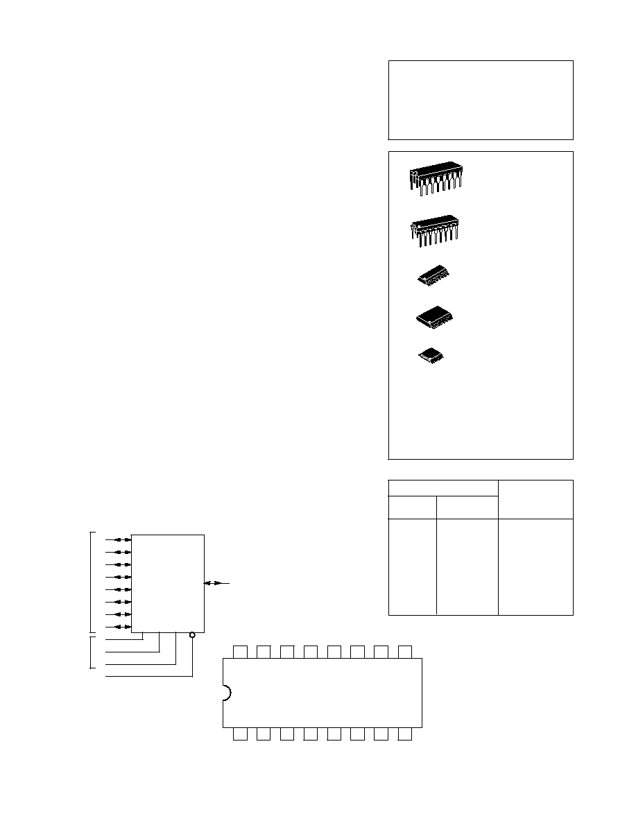
D SUFFIX
SOIC PACKAGE
CASE 751B≠05
N SUFFIX
PLASTIC PACKAGE
CASE 648≠08
1
16
1
16
J SUFFIX
CERAMIC PACKAGE
CASE 620≠10
1
16
ORDERING INFORMATION
MC54HCXXXXJ
MC74HCXXXXN
MC74HCXXXXD
MC74HCXXXXDW
MC74HCXXXXDT
Ceramic
Plastic
SOIC
SOIC Wide
TSSOP
1
16
DT SUFFIX
TSSOP PACKAGE
CASE 948F≠01
DW SUFFIX
SOIC PACKAGE
CASE 751G≠02
1
16

MC54/74HC4051 MC74HC4052 MC54/74HC4053
LOGIC DIAGRAM
MC74HC4052
Double≠Pole, 4≠Position Plus Common Off
X0
12
X1
14
X2
15
X3
11
Y0
1
Y1
5
Y2
2
Y3
4
A
10
B
9
ENABLE
6
X SWITCH
Y SWITCH
X
13
ANALOG
INPUTS/OUTPUTS
CHANNEL SELECT
INPUTS
PIN 16 = V
CC
PIN 7 = V
EE
PIN 8 = GND
COMMON
OUTPUTS/INPUTS
L
L
H
H
X
L
H
L
H
X
FUNCTION TABLE ≠ MC74HC4052
Control Inputs
ON Channels
Enable
Select
B
A
X0
X1
X2
X3
L
L
L
L
H
X = Don't Care
Pinout: MC74HC4052 (Top View)
15
16
14
13
12
11
10
2
1
3
4
5
6
7
V
CC
9
8
X2
X1
X
X0
X3
A
B
Y0
Y2
Y
Y3
Y1 Enable V
EE
GND
Y
3
Y0
Y1
Y2
Y3
NONE
LOGIC DIAGRAM
MC54/74HC4053
Triple Single≠Pole, Double≠Position Plus Common Off
X0
12
X1
13
A
11
B
10
C
9
ENABLE
6
X SWITCH
Y SWITCH
X
14
ANALOG
INPUTS/OUTPUTS
CHANNEL SELECT
INPUTS
PIN 16 = V
CC
PIN 7 = V
EE
PIN 8 = GND
COMMON
OUTPUTS/INPUTS
L
L
L
L
H
H
H
H
X
L
L
H
H
L
L
H
H
X
L
H
L
H
L
H
L
H
X
FUNCTION TABLE ≠ MC54/74HC4053
Control Inputs
ON Channels
Enable
Select
C
B
A
L
L
L
L
L
L
L
L
H
X = Don't Care
Pinout: MC54/74HC4053 (Top View)
15
16
14
13
12
11
10
2
1
3
4
5
6
7
V
CC
9
8
Y
X
X1
X0
A
B
C
Y1
Y0
Z1
Z
Z0 Enable V
EE
GND
Z0
Z0
Z0
Z0
Z1
Z1
Z1
Z1
Y0
Y0
Y1
Y1
Y0
Y0
Y1
Y1
X0
X1
X0
X1
X0
X1
X0
X1
NONE
Y0
2
Y1
1
Y
15
Z0
5
Z1
3
Z
4
Z SWITCH
NOTE: This device allows independent control of each switch.
Channel≠Select Input A controls the X≠Switch, Input B controls
the Y≠Switch and Input C controls the Z≠Switch

MC54/74HC4051 MC74HC4052 MC54/74HC4053
ŒŒŒŒŒŒŒŒŒŒŒŒŒŒŒŒŒŒŒŒŒŒŒ
ŒŒŒŒŒŒŒŒŒŒŒŒŒŒŒŒŒŒŒŒŒŒŒ
MAXIMUM RATINGS*
ŒŒŒ
ŒŒŒ
Symbol
ŒŒŒŒŒŒŒŒŒŒŒŒŒŒ
ŒŒŒŒŒŒŒŒŒŒŒŒŒŒ
Parameter
ŒŒŒŒŒŒ
ŒŒŒŒŒŒ
Value
ŒŒŒ
ŒŒŒ
Unit
ŒŒŒ
Œ
Œ
Œ
ŒŒŒ
V
CC
ŒŒŒŒŒŒŒŒŒŒŒŒŒŒ
Œ
ŒŒŒŒŒŒŒŒŒŒŒŒ
Œ
ŒŒŒŒŒŒŒŒŒŒŒŒŒŒ
Positive DC Supply Voltage
(Referenced to GND)
(Referenced to V
EE
)
ŒŒŒŒŒŒ
Œ
ŒŒŒŒ
Œ
ŒŒŒŒŒŒ
≠ 0.5 to + 7.0
≠ 0.5 to + 14.0
ŒŒŒ
Œ
Œ
Œ
ŒŒŒ
V
ŒŒŒ
ŒŒŒ
V
EE
ŒŒŒŒŒŒŒŒŒŒŒŒŒŒ
ŒŒŒŒŒŒŒŒŒŒŒŒŒŒ
Negative DC Supply Voltage (Referenced to GND)
ŒŒŒŒŒŒ
ŒŒŒŒŒŒ
≠ 7.0 to + 5.0
ŒŒŒ
ŒŒŒ
V
ŒŒŒ
Œ
Œ
Œ
ŒŒŒ
V
IS
ŒŒŒŒŒŒŒŒŒŒŒŒŒŒ
Œ
ŒŒŒŒŒŒŒŒŒŒŒŒ
Œ
ŒŒŒŒŒŒŒŒŒŒŒŒŒŒ
Analog Input Voltage
ŒŒŒŒŒŒ
Œ
ŒŒŒŒ
Œ
ŒŒŒŒŒŒ
V
EE
≠ 0.5 to
V
CC
+ 0.5
ŒŒŒ
Œ
Œ
Œ
ŒŒŒ
V
ŒŒŒ
ŒŒŒ
V
in
ŒŒŒŒŒŒŒŒŒŒŒŒŒŒ
ŒŒŒŒŒŒŒŒŒŒŒŒŒŒ
Digital Input Voltage (Referenced to GND)
ŒŒŒŒŒŒ
ŒŒŒŒŒŒ
≠ 0.5 to V
CC
+ 0.5
ŒŒŒ
ŒŒŒ
V
ŒŒŒ
ŒŒŒ
I
ŒŒŒŒŒŒŒŒŒŒŒŒŒŒ
ŒŒŒŒŒŒŒŒŒŒŒŒŒŒ
DC Current, Into or Out of Any Pin
ŒŒŒŒŒŒ
ŒŒŒŒŒŒ
±
25
ŒŒŒ
ŒŒŒ
mA
ŒŒŒ
Œ
Œ
Œ
ŒŒŒ
P
D
ŒŒŒŒŒŒŒŒŒŒŒŒŒŒ
Œ
ŒŒŒŒŒŒŒŒŒŒŒŒ
Œ
ŒŒŒŒŒŒŒŒŒŒŒŒŒŒ
Power Dissipation in Still Air, Plastic or Ceramic DIP
SOIC Package
TSSOP Package
ŒŒŒŒŒŒ
Œ
ŒŒŒŒ
Œ
ŒŒŒŒŒŒ
750
500
450
ŒŒŒ
Œ
Œ
Œ
ŒŒŒ
mW
ŒŒŒ
ŒŒŒ
T
stg
ŒŒŒŒŒŒŒŒŒŒŒŒŒŒ
ŒŒŒŒŒŒŒŒŒŒŒŒŒŒ
Storage Temperature Range
ŒŒŒŒŒŒ
ŒŒŒŒŒŒ
≠ 65 to + 150
ŒŒŒ
ŒŒŒ
_
C
ŒŒŒ
Œ
Œ
Œ
ŒŒŒ
T
L
ŒŒŒŒŒŒŒŒŒŒŒŒŒŒ
Œ
ŒŒŒŒŒŒŒŒŒŒŒŒ
Œ
ŒŒŒŒŒŒŒŒŒŒŒŒŒŒ
Lead Temperature, 1 mm from Case for 10 Seconds
Plastic DIP, SOIC or TSSOP Package
Ceramic DIP
ŒŒŒŒŒŒ
Œ
ŒŒŒŒ
Œ
ŒŒŒŒŒŒ
260
300
ŒŒŒ
Œ
Œ
Œ
ŒŒŒ
_
C
* Maximum Ratings are those values beyond which damage to the device may occur.
Functional operation should be restricted to the Recommended Operating Conditions.
Derating -- Plastic DIP: ≠ 10 mW/
_
C from 65
_
to 125
_
C
Ceramic DIP: ≠ 10 mW/
_
C from 100
_
to 125
_
C
SOIC Package: ≠ 7 mW/
_
C from 65
_
to 125
_
C
TSSOP Package: ≠ 6.1 mW/
_
C from 65
_
to 125
_
C
RECOMMENDED OPERATING CONDITIONS
ŒŒŒŒ
ŒŒŒŒ
Symbol
ŒŒŒŒŒŒŒŒŒŒŒŒŒŒ
ŒŒŒŒŒŒŒŒŒŒŒŒŒŒ
Parameter
ŒŒŒ
ŒŒŒ
Min
ŒŒŒ
ŒŒŒ
Max
ŒŒŒ
ŒŒŒ
Unit
ŒŒŒŒ
Œ
ŒŒ
Œ
ŒŒŒŒ
V
CC
ŒŒŒŒŒŒŒŒŒŒŒŒŒŒ
Œ
ŒŒŒŒŒŒŒŒŒŒŒŒ
Œ
ŒŒŒŒŒŒŒŒŒŒŒŒŒŒ
Positive DC Supply Voltage
(Referenced to GND)
(Referenced to V
EE
)
ŒŒŒ
Œ
Œ
Œ
ŒŒŒ
2.0
2.0
ŒŒŒ
Œ
Œ
Œ
ŒŒŒ
6.0
12.0
ŒŒŒ
Œ
Œ
Œ
ŒŒŒ
V
ŒŒŒŒ
ŒŒŒŒ
V
EE
ŒŒŒŒŒŒŒŒŒŒŒŒŒŒ
ŒŒŒŒŒŒŒŒŒŒŒŒŒŒ
Negative DC Supply Voltage, Output (Referenced to
GND)
ŒŒŒ
ŒŒŒ
≠ 6.0
ŒŒŒ
ŒŒŒ
GND
ŒŒŒ
ŒŒŒ
V
ŒŒŒŒ
ŒŒŒŒ
V
IS
ŒŒŒŒŒŒŒŒŒŒŒŒŒŒ
ŒŒŒŒŒŒŒŒŒŒŒŒŒŒ
Analog Input Voltage
ŒŒŒ
ŒŒŒ
V
EE
ŒŒŒ
ŒŒŒ
V
CC
ŒŒŒ
ŒŒŒ
V
ŒŒŒŒ
ŒŒŒŒ
V
in
ŒŒŒŒŒŒŒŒŒŒŒŒŒŒ
ŒŒŒŒŒŒŒŒŒŒŒŒŒŒ
Digital Input Voltage (Referenced to GND)
ŒŒŒ
ŒŒŒ
GND
ŒŒŒ
ŒŒŒ
V
CC
ŒŒŒ
ŒŒŒ
V
ŒŒŒŒ
ŒŒŒŒ
V
IO
*
ŒŒŒŒŒŒŒŒŒŒŒŒŒŒ
ŒŒŒŒŒŒŒŒŒŒŒŒŒŒ
Static or Dynamic Voltage Across Switch
ŒŒŒ
ŒŒŒ
ŒŒŒ
ŒŒŒ
1.2
ŒŒŒ
ŒŒŒ
V
ŒŒŒŒ
ŒŒŒŒ
T
A
ŒŒŒŒŒŒŒŒŒŒŒŒŒŒ
ŒŒŒŒŒŒŒŒŒŒŒŒŒŒ
Operating Temperature Range, All Package Types
ŒŒŒ
ŒŒŒ
≠ 55
ŒŒŒ
ŒŒŒ
+ 125
ŒŒŒ
ŒŒŒ
_
C
ŒŒŒŒ
Œ
ŒŒ
Œ
Œ
ŒŒ
Œ
ŒŒŒŒ
t
r
, t
f
ŒŒŒŒŒŒŒŒŒŒŒŒŒŒ
Œ
ŒŒŒŒŒŒŒŒŒŒŒŒ
Œ
Œ
ŒŒŒŒŒŒŒŒŒŒŒŒ
Œ
ŒŒŒŒŒŒŒŒŒŒŒŒŒŒ
Input Rise/Fall Time
V
CC
= 2.0 V
(Channel Select or Enable Inputs)
V
CC
= 4.5 V
V
CC
= 6.0 V
ŒŒŒ
Œ
Œ
Œ
Œ
Œ
Œ
ŒŒŒ
0
0
0
ŒŒŒ
Œ
Œ
Œ
Œ
Œ
Œ
ŒŒŒ
1000
500
400
ŒŒŒ
Œ
Œ
Œ
Œ
Œ
Œ
ŒŒŒ
ns
* For voltage drops across switch greater than 1.2V (switch on), excessive V
CC
current may be
drawn; i.e., the current out of the switch may contain both V
CC
and switch input components. The
reliability of the device will be unaffected unless the Maximum Ratings are exceeded.
This device contains protection
circuitry to guard against damage
due to high static voltages or electric
fields. However, precautions must
be taken to avoid applications of any
voltage higher than maximum rated
voltages to this high≠impedance cir-
cuit. For proper operation, V
in
and
V
out
should be constrained to the
range GND
v
(V
in
or V
out
)
v
V
CC
.
Unused inputs must always be
tied to an appropriate logic voltage
level (e.g., either GND or V
CC
).
Unused outputs must be left open.

MC54/74HC4051 MC74HC4052 MC54/74HC4053
DC CHARACTERISTICS -- Digital Section
(Voltages Referenced to GND) V
EE
= GND, Except Where Noted
V
CC
Guaranteed Limit
Symbol
Parameter
Condition
V
CC
V
≠55 to 25
∞
C
85
∞
C
125
∞
C
Unit
V
IH
Minimum High≠Level Input Voltage,
Channel≠Select or Enable Inputs
R
on
= Per Spec
2.0
4.5
6.0
1.50
3.15
4.20
1.50
3.15
4.20
1.50
3.15
4.20
V
V
IL
Maximum Low≠Level Input Voltage,
Channel≠Select or Enable Inputs
R
on
= Per Spec
2.0
4.5
6.0
0.3
0.9
1.2
0.3
0.9
1.2
0.3
0.9
1.2
V
I
in
Maximum Input Leakage Current,
Channel≠Select or Enable Inputs
V
in
= V
CC
or GND,
V
EE
= ≠ 6.0 V
6.0
±
0.1
±
1.0
±
1.0
µ
A
I
CC
Maximum Quiescent Supply
Current (per Package)
Channel Select, Enable and
V
IS
= V
CC
or GND;
V
EE
= GND
V
IO
= 0 V
V
EE
= ≠ 6.0
6.0
6.0
2
8
20
80
40
160
µ
A
DC CHARACTERISTICS -- Analog Section
Guaranteed Limit
Symbol
Parameter
Condition
V
CC
V
EE
≠55 to 25
∞
C
85
∞
C
125
∞
C
Unit
R
on
Maximum "ON" Resistance
V
in
= V
IL
or V
IH
; V
IS
= V
CC
to
V
EE
; I
S
2.0 mA
(Figures 1, 2)
4.5
4.5
6.0
0.0
≠ 4.5
≠ 6.0
190
120
100
240
150
125
280
170
140
V
in
= V
IL
or V
IH
; V
IS
= V
CC
or
V
EE
(Endpoints); I
S
2.0 mA
(Figures 1, 2)
4.5
4.5
6.0
0.0
≠ 4.5
≠ 6.0
150
100
80
190
125
100
230
140
115
R
on
Maximum Difference in "ON"
Resistance Between Any Two
Channels in the Same Package
V
in
= V
IL
or V
IH
;
V
IS
= 1/2 (V
CC
≠ V
EE
);
I
S
2.0 mA
4.5
4.5
6.0
0.0
≠ 4.5
≠ 6.0
30
12
10
35
15
12
40
18
14
I
off
Maximum Off≠Channel Leakage
Current, Any One Channel
V
in
= V
IL
or V
IH
;
V
IO
= V
CC
≠ V
EE
;
Switch Off (Figure 3)
6.0
≠ 6.0
0.1
0.5
1.0
µ
A
Maximum Off≠Channel
HC4051
Leakage Current,
HC4052
Common Channel
HC4053
V
in
= V
IL
or V
IH
;
V
IO
= V
CC
≠ V
EE
;
Switch Off (Figure 4)
6.0
6.0
6.0
≠ 6.0
≠ 6.0
≠ 6.0
0.2
0.1
0.1
2.0
1.0
1.0
4.0
2.0
2.0
I
on
Maximum On≠Channel
HC4051
Leakage Current,
HC4052
Channel≠to≠Channel
HC4053
V
in
= V
IL
or V
IH
;
Switch≠to≠Switch =
V
CC
≠ V
EE
; (Figure 5)
6.0
6.0
6.0
≠ 6.0
≠ 6.0
≠ 6.0
0.2
0.1
0.1
2.0
1.0
1.0
4.0
2.0
2.0
µ
A