©
Semiconductor Components Industries, LLC, 2004
September, 2004 - Rev. 6
1
Publication Order Number:
MKP1V120/D
MKP1V120 Series
Preferred Device
Sidac High Voltage
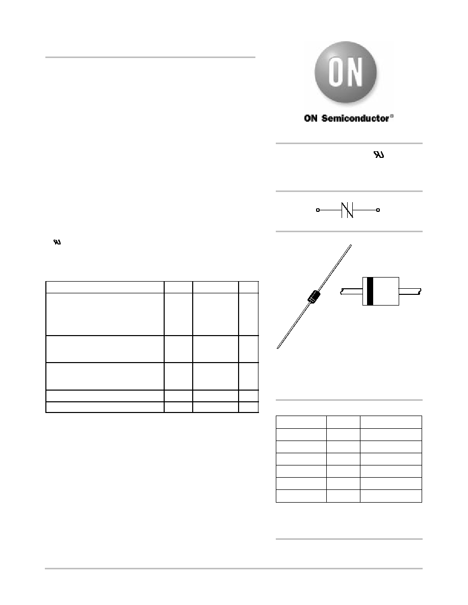
Bidirectional Triggers
Bidirectional devices designed for direct interface with the ac power
line. Upon reaching the breakover voltage in each direction, the device
switches from a blocking state to a low voltage on-state. Conduction
will continue like a Triac until the main terminal current drops below
the holding current. The plastic axial lead package provides high pulse
current capability at low cost. Glass passivation insures reliable
operation. Applications are:
∑
High Pressure Sodium Vapor Lighting
∑
Strobes and Flashers
∑
Ignitors
∑
High Voltage Regulators
∑
Pulse Generators
∑
Used to Trigger Gates of SCR's and Triacs
∑
Indicates UL Registered -- File #E116110
∑
Device Marking: Logo, Device Type, e.g., MKP1V120, Date Code
MAXIMUM RATINGS
(T
J
= 25
∞
C unless otherwise noted)
Rating
Symbol
Value
Unit
Peak Repetitive Off-State Voltage
(Sine Wave, 50 to 60 Hz,
T
J
= - 40 to 125
∞
C)
MKP1V120, MKP1V130, MKP1V160
MKP1V240
V
DRM
,
V
RRM
"
90
"
180
V
On-State Current RMS
(T
L
= 80
∞
C, Lead Length = 3/8
,
All Conduction Angles)
I
T(RMS)
"
0.9
A
Peak Non-repetitive Surge Current
(60 Hz One Cycle Sine Wave,
T
J
= 125
∞
C)
I
TSM
"
4.0
A
Operating Junction Temperature Range
T
J
- 40 to +125
∞
C
Storage Temperature Range
T
stg
- 40 to +150
∞
C
Maximum ratings are those values beyond which device damage can occur.
Maximum ratings applied to the device are individual stress limit values (not
normal operating conditions) and are not valid simultaneously. If these limits are
exceeded, device functional operation is not implied, damage may occur and
reliability may be affected.
SIDACS
0.9 AMPS RMS
120 - 240 V
Preferred devices are recommended choices for future use
and best overall value.
Device
Package
Shipping
ORDERING INFORMATION
MKP1V120RL
DO-41
5000 Tape & Reel
MT1
MT2
MKP1V130RL
DO-41
MKP1V160
DO-41
1000 Units / Bulk
MKP1V160RL
DO-41
MKP1V240
DO-41
MKP1V240RL
DO-41
(
)
http://onsemi.com
5000 Tape & Reel
5000 Tape & Reel
5000 Tape & Reel
1000 Units / Bulk
For information on tape and reel specifications,
including part orientation and tape sizes, please
refer to our Tape and Reel Packaging Specifications
Brochure, BRD8011/D.
AXIAL LEAD
CASE 59-10
DO-41
PLASTIC
MARKING
DIAGRAM
MKP
1V1xx0
AYYW
xx
= 12, 13, 16 or 24
A
= Assembly Location
YY
= Year
W
= Work Week

MKP1V120 Series
http://onsemi.com
2
THERMAL CHARACTERISTICS
Characteristic
Symbol
Max
Unit
Thermal Resistance, Junction-to-Lead
Lead Length = 3/8
R
q
JL
40
∞
C/W
Lead Solder Temperature
(Lead Length
w
1/16
from Case, 10 s Max)
T
L
260
∞
C
ELECTRICAL CHARACTERISTICS
(T
C
= 25
∞
C unless otherwise noted; Electricals apply in both directions)
Characteristic
Symbol
Min
Typ
Max
Unit
OFF CHARACTERISTICS
Repetitive Peak Off-State Current
T
J
= 25
∞
C
(50 to 60 Hz Sine Wave)
V
DRM
= 90 V, MKP1V120, MKP1V130 and MKP1V160
V
DRM
= 180 V, MKP1V240
I
DRM
-
-
5.0
m
A
ON CHARACTERISTICS
Breakover Voltage
I
BO
= 35
m
A
MKP1V120
35
m
A
MKP1V130
200
m
A
MKP1V160
35
m
A
MKP1V240
V
BO
110
120
150
220
-
-
130
140
170
250
Volts
Peak On-State Voltage
(I
TM
= 1 A Peak, Pulse Width
300
m
s, Duty Cycle
2%)
V
TM
-
1.3
1.5
Volts
Dynamic Holding Current
(Sine Wave, 50 to 60 Hz, R
L
= 100 Ohm)
I
H
-
-
100
mA
Switching Resistance
(Sine Wave, 50 to 60 Hz)
R
S
0.1
-
-
k
W
DYNAMIC CHARACTERISTICS
Critical Rate-of-Rise of On-State Current,
Critical Damped Waveform Circuit
(I
PK
= 130 Amps, Pulse Width = 10
m
sec)
di/dt
-
120
-
A/
m
s
MKP1V120 Series
http://onsemi.com
3
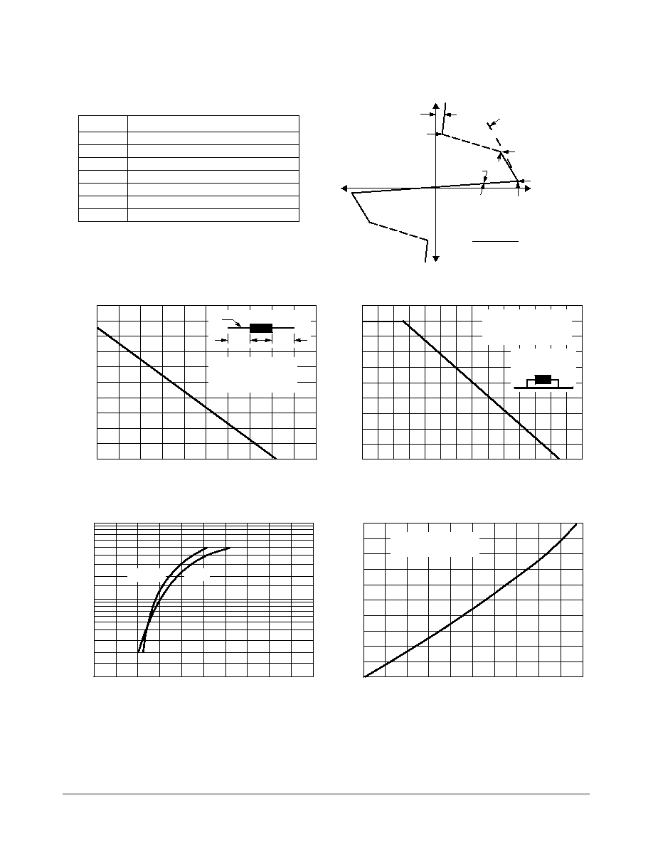
+ Current
+ Voltage
V
TM
I
H
Symbol
Parameter
I
DRM
Off State Leakage Current
V
DRM
Off State Repetitive Blocking Voltage
V
BO
Breakover Voltage
I
BO
Breakover Current
I
H
Holding Current
V
TM
On State Voltage
I
TM
Peak on State Current
Voltage Current Characteristic of SIDAC
V
DRM
I
DRM
I
TM
Slope = R
S
V
(BO)
R
S
+
(V
(BO)
≠ V
S
)
(I
S
≠ I
(BO)
)
I
(BO)
I
S
V
S
(Bidirectional Device)
0.8
0
I
T(RMS)
, ON-STATE CURRENT (AMPS)
140
120
40
T
A
, MAXIMUM AMBIENT TEMPERATURE (
∞
C)
0.4
2.0
3.0
0
V
T
, INSTANTANEOUS ON-STATE VOLTAGE (VOLTS)
0.3
0.5
0.2
0.1
1.0
T
4.0
0.2
0.6
I
100
0.7
1.0
130
, MAXIMUM
ALLOW
ABLE LEAD
TEMPERA
TURE ( C)
L
100
0
1.0
0.6
0.2
40
I
20
60
0.4
0.8
, ON-ST
A
TE CURRENT
(AMPS)
T(RMS)
0.2
0.6
0
I
T(RMS)
, ON-STATE CURRENT (AMPS)
0.50
0.75
0.25
0.4
0.8
P
1.00
1.25
T
J
= 25
∞
C
Conduction Angle = 180
∞
C
1.6
1.2
1.0
1.4
2.0
1.8
110
90
80
60
70
50
∞
80
120
140
5.0
3.0
5.0
2.0
7.0
10
, INST
ANT
ANEOUS ON-ST
A
TE CURRENT
(AMPS)
T
1.0
, POWER DISSIP
A
TION (W
A
TTS)
RMS
T
J
= 25
∞
C
125
∞
C
T
J
= 125
∞
C
Sine Wave
Conduction Angle = 180
∞
C
Assembled in PCB
Lead Length =
3
/
8
T
J
= 125
∞
C
Sine Wave
Conduction Angle = 180
∞
C
T
L
3
/
8
3
/
8
Figure 1. Maximum Lead Temperature
Figure 2. Maximum Ambient Temperature
Figure 3. Typical On-State Voltage
Figure 4. Typical Power Dissipation
THERMAL CHARACTERISTICS
MKP1V120 Series
http://onsemi.com
4
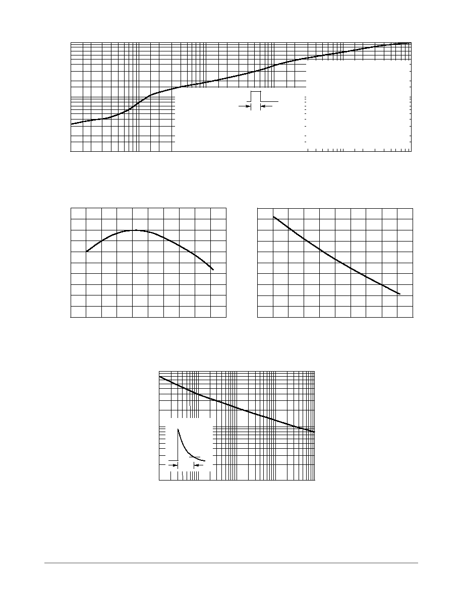
Figure 5. Thermal Response
t, TIME (ms)
10
0.1
0.07
0.03
0.02
0.01
5.0
0.2
0.5
1.0
2.0
0.05
0.1
0.2
r(t),
TRANSIENT
THERMAL
RESIST
ANCE (NORMALIZED)
0.3
0.5
0.7
1.0
20
50
100
200
500
1.0 k
2.0 k
5.0 k
10 k
The temperature of the lead should be
measured using a thermocouple placed on the
lead as close as possible to the tie point. The
thermal mass connected to the tie point is
normally large enough so that it will not
significantly respond to heat surges generated
in the diode as a result of pulsed operation
once steady-state conditions are achieved.
Using the measured value of T
L
, the junction
temperature may be determined by:
T
J
= T
L
+
DT
JL
Z
qJL
(t) = R
qJL
∑
r(t)
DT
JL
= P
pk
R
qJL
[r(t)]
where:
DT
JL
= the increase in junction temperature above the
lead temperature
r(t) = normalized value of transient thermal resistance at
time, t from this figure. For example,
r(t
p
) = normalized value of transient resistance at time t
p
.
TIME
t
p
Figure 6. Typical Breakover Voltage
Figure 7. Typical Holding Current
Figure 8. Pulse Rating Curve
T
J
, JUNCTION TEMPERATURE (
∞
C)
-60
0.8
0.4
100
0.1
t
w
, PULSE WIDTH (ms)
100
10
1.0
I
-40
-20
100
140
0.6
1.0
1.2
10
T
J
, JUNCTION TEMPERATURE (
∞
C)
100
-60
0.9
0.8
V
40
-40
-20
0
20
1.0
1.4
, BREAKOVER VOL
T
AGE (NORMALIZED)
BO
1.0
I PK
, PEAK CURRENT
(AMPS)
80
60
120
140
, HOLDING CURRENT
(NORMALIZED)
H
120
80
0
60
40
20
10%
tw
I
PK
MKP1V120 Series
http://onsemi.com
5
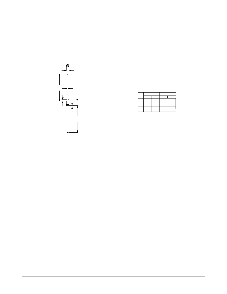
PACKAGE DIMENSIONS
B
D
K
K
F
F
A
DIM
MIN
MAX
MIN
MAX
MILLIMETERS
INCHES
A
4.10
5.20
0.161
0.205
B
2.00
2.70
0.079
0.106
D
0.71
0.86
0.028
0.034
F
---
1.27
---
0.050
K
25.40
---
1.000
---
NOTES:
1. DIMENSIONING AND TOLERANCING PER ANSI
Y14.5M, 1982.
2. CONTROLLING DIMENSION: INCH.
3. 59-04 OBSOLETE, NEW STANDARD 59-09.
4. 59-03 OBSOLETE, NEW STANDARD 59-10.
5. ALL RULES AND NOTES ASSOCIATED WITH
JEDEC DO-41 OUTLINE SHALL APPLY
6. POLARITY DENOTED BY CATHODE BAND.
7. LEAD DIAMETER NOT CONTROLLED WITHIN F
DIMENSION.
DO-41
PLASTIC AXIAL
(No Polarity)
CASE 059A-01
ISSUE A