 | –≠–ª–µ–∫—Ç—Ä–æ–Ω–Ω—ã–π –∫–æ–º–ø–æ–Ω–µ–Ω—Ç: NTF6P02T3 | –°–∫–∞—á–∞—Ç—å:  PDF PDF  ZIP ZIP |

Publication Order Number:
NTF6P02T3/D
©
Semiconductor Components Industries, LLC, 2002
September, 2002 ≠ Rev. 0
1
NTF6P02T3
Power MOSFET
-6.0 Amps, -20 Volts
P≠Channel SOT≠223
Features
∑
Low R
DS(on)
∑
Logic Level Gate Drive
∑
Diode Exhibits High Speed, Soft Recovery
∑
Avalanche Energy Specified
Typical Applications
∑
Power Management in Portables and Battery≠Powered Products, i.e.:
Cellular and Cordless Telephones and PCMCIA Cards
MAXIMUM RATINGS
(T
J
= 25
∞
C unless otherwise noted)
Rating
Symbol
Value
Unit
Drain≠to≠Source Voltage
V
DSS
≠20
Vdc
Gate≠to≠Source Voltage
V
GS
±
8.0
Vdc
Drain Current (Note 1)
≠ Continuous @ T
A
= 25
∞
C
≠ Continuous @ T
A
= 70
∞
C
≠ Single Pulse (t
p
= 10
µ
s)
I
D
I
D
I
DM
≠10
≠8.4
≠35
Adc
Apk
Total Power Dissipation @ T
A
= 25
∞
C
P
D
8.3
W
Operating and Storage Temperature Range
T
J
, T
stg
≠55 to
+150
∞
C
Single Pulse Drain≠to≠Source Avalanche
Energy ≠ Starting T
J
= 25
∞
C
(V
DD
= ≠20 Vdc, V
GS
= ≠5.0 Vdc,
I
L(pk)
= ≠10 A, L = 3.0 mH, R
G
= 25
W
)
E
AS
150
mJ
Thermal Resistance
≠ Junction to Lead (Note 1)
≠ Junction to Ambient (Note 2)
≠ Junction to Ambient (Note 3)
R
JL
R
JA
R
JA
15
71.4
160
∞
C/W
Maximum Lead Temperature for Soldering
Purposes, 1/8
from case for 10 seconds
T
L
260
∞
C
1. Steady State.
2. When surface mounted to an FR4 board using 1
pad size,
(Cu. Area 1.127 in
2
), Steady State.
3. When surface mounted to an FR4 board using minimum recommended pad
size, (Cu. Area 0.412 in
2
), Steady State.
D
G
S
1
2
3
4
≠6.0 AMPERES
≠20 VOLTS
R
DS(on)
= 44 m
W
(Typ.)
P≠Channel
Device
Package
Shipping
ORDERING INFORMATION
NTF6P02T3
SOT≠223
4000/Tape & Reel
SOT≠223
CASE 318E
STYLE 3
6P02
MARKING
DIAGRAM
AWW
A
= Assembly Location
WW
= Work Week
6P02
= Device Code
PIN ASSIGNMENT
3
2
1
Gate
Drain Source
4 Drain
http://onsemi.com

NTF6P02T3
http://onsemi.com
2
ELECTRICAL CHARACTERISTICS
(T
J
= 25
∞
C unless otherwise noted)
Characteristic
Symbol
Min
Typ
Max
Unit
OFF CHARACTERISTICS
Drain≠to≠Source Breakdown Voltage (Note 4)
(V
GS
= 0 Vdc,
I
D
= ≠250
m
Adc)
Temperature Coefficient (Positive)
V
(BR)DSS
≠20
≠
≠25
≠11
≠
≠
Vdc
mV/
∞
C
Zero Gate Voltage Drain Current
(V
DS
= ≠20 Vdc, V
GS
= 0 Vdc)
(V
DS
= ≠20 Vdc, V
GS
= 0 Vdc, T
J
= 125
∞
C)
I
DSS
≠
≠
≠
≠
≠1.0
≠10
m
Adc
Gate≠Body Leakage Current
(V
GS
=
±
8.0 Vdc, V
DS
= 0 Vdc)
I
GSS
≠
≠
±
100
nAdc
ON CHARACTERISTICS
(Note 4)
Gate Threshold Voltage (Note 4)
(V
DS
= V
GS
,
I
D
= ≠250
m
Adc)
Threshold Temperature Coefficient (Negative)
V
GS(th)
≠0.4
≠
≠0.7
2.6
≠1.0
≠
Vdc
mV/
∞
C
Static Drain≠to≠Source On≠Resistance (Note 4)
(V
GS
= ≠4.5 Vdc, I
D
= ≠6.0 Adc)
(V
GS
= ≠2.5 Vdc, I
D
= ≠4.0 Adc)
(V
GS
= ≠2.5 Vdc, I
D
= ≠3.0 Adc)
R
DS(on)
≠
≠
≠
44
57
57
50
70
≠
m
W
Forward Transconductance
(Note 4)
(V
DS
= ≠10 Vdc, I
D
= ≠6.0 Adc)
g
fs
≠
12
≠
Mhos
DYNAMIC CHARACTERISTICS
Input Capacitance
(V
DS
= ≠16 Vdc, V
GS
= 0 V,
f
1 0 MH )
C
iss
≠
900
1200
pF
Output Capacitance
f = 1.0 MHz)
C
oss
≠
350
500
Transfer Capacitance
C
rss
≠
90
150
Input Capacitance
(V
DS
= ≠10 Vdc, V
GS
= 0 V,
f
1 0 MH )
C
iss
≠
940
≠
pF
Output Capacitance
f = 1.0 MHz)
C
oss
≠
410
≠
Transfer Capacitance
C
rss
≠
110
≠
SWITCHING CHARACTERISTICS
(Note 5)
Turn≠On Delay Time
(V
DD
= ≠5.0 Vdc, I
D
= ≠1.0 Adc,
V
4 5 Vd
t
d(on)
≠
7.0
12
ns
Rise Time
V
GS
= ≠4.5 Vdc,
R
G
= 6.0
W
)
t
r
≠
25
45
Turn≠Off Delay Time
R
G
= 6.0
W
)
t
d(off)
≠
75
125
Fall Time
t
f
≠
50
85
Turn≠On Delay Time
(V
DD
= ≠16 Vdc, I
D
= ≠6.0 Adc,
V
4 5 Vd
t
d(on)
≠
8.0
≠
ns
Rise Time
V
GS
= ≠4.5 Vdc,
R
G
= 2.5
W
)
t
r
≠
30
≠
Turn≠Off Delay Time
R
G
= 2.5
W
)
t
d(off)
≠
60
≠
Fall Time
t
f
≠
60
≠
Gate Charge
(V
DS
= ≠16 Vdc, I
D
= ≠6.0 Adc,
V
4 5 Vd ) (N t 4)
Q
T
≠
15
20
nC
V
GS
= ≠4.5 Vdc) (Note 4)
Q
gs
≠
1.7
≠
Q
gd
≠
6.0
≠
SOURCE≠DRAIN DIODE CHARACTERISTICS
Forward On≠Voltage
(I
S
= ≠3.0 Adc, V
GS
= 0 Vdc) (Note 4)
(I
S
= ≠2.1 Adc, V
GS
= 0 Vdc)
(I
S
= ≠3.0 Adc, V
GS
= 0 Vdc, T
J
= 125
∞
C)
V
SD
≠
≠
≠
≠0.82
≠0.74
≠0.68
≠1.2
≠
≠
Vdc
Reverse Recovery Time
(I
S
= ≠3.0 Adc, V
GS
= 0 Vdc,
dI /dt
100 A/
) (N t 4)
t
rr
≠
42
≠
ns
dI
S
/dt = 100 A/
m
s) (Note 4)
t
a
≠
17
≠
t
b
≠
25
≠
Reverse Recovery Stored Charge
Q
RR
≠
0.036
≠
m
C
4. Pulse Test: Pulse Width
300
m
s, Duty Cycle
2.0%.
5. Switching characteristics are independent of operating junction temperatures.

NTF6P02T3
http://onsemi.com
3
TYPICAL ELECTRICAL CHARACTERISTICS
12
0
6
2
8
4
Figure 1. On≠Region Characteristics
Figure 2. Transfer Characteristics
Figure 3. On≠Resistance versus
Gate≠to≠Source Voltage
Figure 4. On≠Resistance versus Drain Current
and Gate Voltage
Figure 5. On≠Resistance Variation with
Temperature
Figure 6. Drain≠to≠Source Leakage Current
versus Voltage
≠V
GS,
GATE≠TO≠SOURCE VOLTAGE (VOLTS)
≠I
D,
DRAIN CURRENT (AMPS)
T
J
= 25
∞
C
T
J
= 100
∞
C
T
J
= ≠55
∞
C
0
0.2
0.15
0
1
3
≠V
GS,
GATE≠TO≠SOURCE VOLTAGE (VOLTS)
R
DS(on),
DRAIN≠T
O≠SOURCE RESIST
ANCE (
W
)
≠I
D,
DRAIN CURRENT (AMPS)
R
DS(on),
DRAIN≠T
O≠SOURCE RESIST
ANCE (
W
)
V
GS
= ≠4.5 V
1.6
1.4
T
J
, JUNCTION TEMPERATURE (
∞
C)
R
DS(on),
DRAIN≠T
O≠SOURCE RESIST
ANCE
(NORMALIZED)
≠50
50
25
0
≠25
75
125
100
I
D
= ≠6.0 A
V
GS
= ≠4.5 V
0.8
0.6
150
100
1000
≠V
DS,
DRAIN≠TO≠SOURCE VOLTAGE (VOLTS)
≠I
DSS
, LEAKAGE (nA)
2
16
20
8
4
6
10,000
6
2
0
3
4
2
1
≠V
DS,
DRAIN≠TO≠SOURCE VOLTAGE (VOLTS)
≠I
D,
DRAIN CURRENT (AMPS)
0
0
3
0.5
2
1
1.5
2.5
0.1
0.05
1.2
0.05
0.04
4
10
8
6
0.03
1.0
T
J
= 100
∞
C
T
J
= 25
∞
C
I
D
= ≠6.0 A
T
J
= 25
∞
C
V
DS
≠10 V
V
GS
= 0 V
3
4
2
T
J
= 150
∞
C
10
V
GS
= ≠1.2 V
≠1.4 V
T
J
= 25
∞
C
0.08
12
14
V
GS
= ≠2.5 V
≠1.6 V
≠1.8 V
≠2.0 V
≠2.2 V
≠3.2 V
≠4.4 V
≠5.0 V
≠7.0 V
≠10 V
6
9
12
≠2.4 V
10
5
0.02
0.06
0.07
14
10
12
18
5
8
6
7
9

NTF6P02T3
http://onsemi.com
4
TYPICAL ELECTRICAL CHARACTERISTICS
≠V
DS
≠V
DS
10
10
0
15
20
≠V
GS
1000
100
10
5
2
1
0
7
0
2400
1800
GATE≠TO≠SOURCE OR DRAIN≠TO≠SOURCE VOLTAGE
(VOLTS)
C, CAP
ACIT
ANCE (pF)
1200
Q
g
, TOTAL GATE CHARGE (nC)
Figure 7. Capacitance Variation
Figure 8. Gate≠to≠Source and
Drain≠to≠Source Voltage versus Total Charge
≠V
GS
, GA
TE≠T
O≠SOURCE VOL
T
AGE (V)
Figure 9. Resistive Switching Time Variation
versus Gate Resistance
R
G
, GATE RESISTANCE (
W
)
Figure 10. Diode Forward Voltage versus Current
≠V
SD
, SOURCE≠TO≠DRAIN VOLTAGE (VOLTS)
≠I
S
, SOURCE CURRENT (AMPS)
t, TIME (ns)
0
8
16
1
10
100
0.3
0.6
1.2
I
D
= ≠6.0 A
T
J
= 25
∞
C
≠V
GS
V
GS
= 0 V
V
DS
= 0 V
T
J
= 25
∞
C
C
rss
C
iss
C
oss
C
rss
1
0.9
C
iss
V
DD
= ≠16 V
I
D
= ≠3.0 A
V
GS
= ≠4.5 V
V
GS
= 0 V
T
J
= 25
∞
C
t
r
t
d(off)
t
d(on)
Q
gd
Q
gs
Q
T
0
12
4
t
f
600
3000
3
4
2
≠V
DS
, DRAIN≠T
O≠SOURCE VOL
T
AGE (V)
0
4
8
12
16
20
5
5
1
3
4
5
6
NTF6P02T3
http://onsemi.com
5
TYPICAL ELECTRICAL CHARACTERISTICS
R
THJ
A
(t)
, EFFECTIVE TRANSIENT
THERMAL RESPONSE
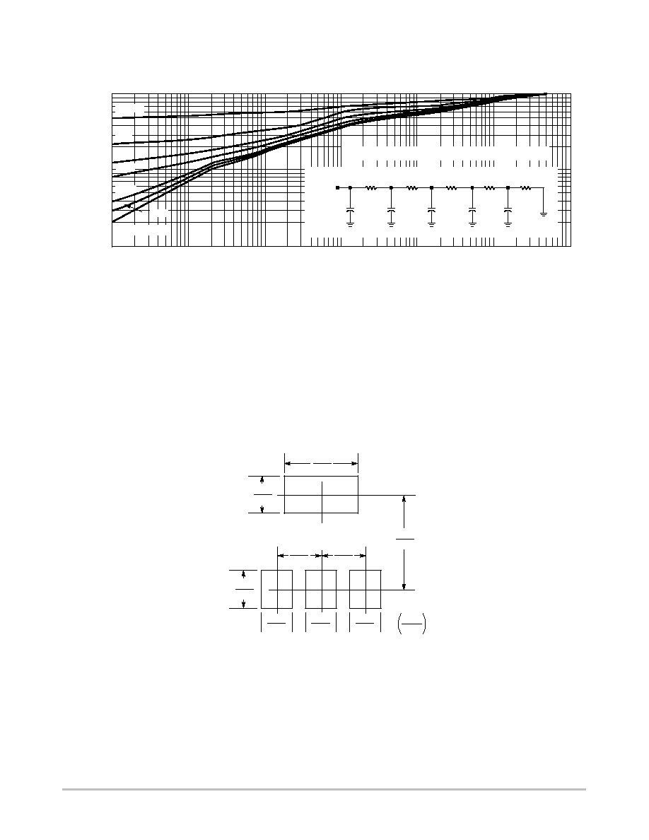
Figure 11. FET Thermal Response
t, TIME (s)
0.1
0.01
D = 0.5
SINGLE PULSE
1.0E-03
1.0E-02
1.0E-01
1.0E+00
1.0E+01
0.2
0.1
0.05
0.02
0.01
1.0E+02
1.0E+03
1
NORMALIZED TO R
q
JA
AT STEADY STATE (1
PAD)
CHIP
JUNCTION
0.0175 W
0.0154 F
0.0710 W
0.0854 F
0.2706 W
0.3074 F
0.5779 W
1.7891 F
0.7086 W
107.55 F
AMBIENT
INFORMATION FOR USING THE SOT≠223 SURFACE MOUNT PACKAGE
MINIMUM RECOMMENDED FOOTPRINT FOR SURFACE MOUNTED APPLICATIONS
Surface mount board layout is a critical portion of the
total design. The footprint for the semiconductor packages
must be the correct size to insure proper solder connection
interface between the board and the package. With the
correct pad geometry, the packages will self align when
subjected to a solder reflow process.
0.079
2.0
0.15
3.8
0.248
6.3
0.079
2.0
0.059
1.5
0.059
1.5
0.059
1.5
0.091
2.3
0.091
2.3
mm
inches