
©
Semiconductor Components Industries, LLC, 2005
July, 2005 - Rev. 13
1
Publication Order Number:
NTHS5441T1/D
NTHS5441
Power MOSFET
-20 V, -5.3 A, P-Channel ChipFET
]
Features
∑
Low R
DS(on)
∑
Higher Efficiency Extending Battery Life
∑
Logic Level Gate Drive
∑
Miniature ChipFET Surface Mount Package
∑
Pb-Free Package is Available
Applications
∑
Power Management in Portable and Battery-Powered Products; i.e.,
Cellular and Cordless Telephones and PCMCIA Cards
MAXIMUM RATINGS
(T
A
= 25
∞
C unless otherwise noted)
Rating
Symbol
5 sec
Steady
State
Unit
Drain-Source Voltage
V
DS
-20
V
Gate-Source Voltage
V
GS
"
12
V
Continuous Drain Current
(T
J
= 150
∞
C) (Note 1)
T
A
= 25
∞
C
T
A
= 85
∞
C
I
D
-5.3
-3.8
-3.9
-2.8
A
Pulsed Drain Current
I
DM
"
20
A
Continuous Source Current
(Note 1)
I
S
-5.3
-3.9
A
Maximum Power Dissipation
(Note 1)
T
A
= 25
∞
C
T
A
= 85
∞
C
P
D
2.5
1.3
1.3
0.7
W
Operating Junction and Storage
Temperature Range
T
J
, T
stg
-55 to +150
∞
C
Maximum ratings are those values beyond which device damage can occur.
Maximum ratings applied to the device are individual stress limit values (not
normal operating conditions) and are not valid simultaneously. If these limits are
exceeded, device functional operation is not implied, damage may occur and
reliability may be affected.
1. Surface Mounted on FR4 Board using 1 in sq pad size (Cu area = 1.27 in sq
[1 oz] including traces).
Device
Package
Shipping
ORDERING INFORMATION
NTHS5441T1
ChipFET
3000/Tape & Reel
G
S
D
P-Channel MOSFET
http://onsemi.com
-20 V
46 m
W
@ -4.5 V
R
DS(on)
TYP
-5.3 A
I
D
MAX
V
(BR)DSS
For information on tape and reel specifications,
including part orientation and tape sizes, please
refer to our Tape and Reel Packaging Specifications
Brochure, BRD8011/D.
NTHS5441T1G
ChipFET
(Pb-Free)
3000/Tape & Reel
S
D
G
D
D
D
D
D
1
2
3
4
5
6
7
8
PIN
CONNECTIONS
ChipFET
CASE 1206A
STYLE 1
MARKING
DIAGRAM
A3
M
G
G
A3 = Specific Device Code
M = Month Code
G
= Pb-Free Package
(Note: Microdot may be in either location)
1
2
3
4
8
7
6
5
1
8

NTHS5441
http://onsemi.com
2
THERMAL CHARACTERISTICS
Characteristic
Symbol
Typ
Max
Unit
Maximum Junction-to-Ambient (Note 2)
t
v
5 sec
Steady State
R
q
JA
40
80
50
95
∞
C/W
Maximum Junction-to-Foot (Drain)
Steady State
R
q
JF
15
20
∞
C/W
ELECTRICAL CHARACTERISTICS
(T
J
= 25
∞
C unless otherwise noted)
Characteristic
Symbol
Test Condition
Min
Typ
Max
Unit
Static
Gate Threshold Voltage
V
GS(th)
V
DS
= V
GS
, I
D
= -250
m
A
-0.6
-1.2
V
Gate-Body Leakage
I
GSS
V
DS
= 0 V, V
GS
=
"
12 V
"
100
nA
Zero Gate Voltage Drain Current
I
DSS
V
DS
= -16 V, V
GS
= 0 V
-1.0
m
A
V
DS
= -16 V, V
GS
= 0 V,
T
J
= 85
∞
C
-5.0
On-State Drain Current (Note 3)
I
D(on)
V
DS
v
-5.0 V, V
GS
= -4.5 V
-20
A
Drain-Source On-State Resistance (Note 3)
r
DS(on)
V
GS
= -3.6 V, I
D
= -3.7 A
V
GS
= -4.5 V, I
D
= -3.9 A
-
-
0.050
0.046
0.06
-
W
V
GS
= -2.5 V, I
D
= -3.1 A
0.070
0.083
Forward Transconductance (Note 3)
g
fs
V
DS
= -10 V, I
D
= -3.9 A
12
mhos
Diode Forward Voltage (Note 3)
V
SD
I
S
= -2.1 A, V
GS
= 0 V
-0.8
-1.2
V
Dynamic (Note 4)
Total Gate Charge
Q
G
V
DS
= -10 V, V
GS
= -4.5 V,
I
D
= -3.9 A
9.7
22
nC
Gate-Source Charge
Q
GS
1.2
Gate-Drain Charge
Q
GD
3.6
Input Capacitance
C
iss
V
DS
= -5.0 Vdc, V
GS
= 0 Vdc,
f = 1.0 MHz
710
pF
Output Capacitance
C
oss
400
Reverse Transfer Capacitance
C
rss
140
Turn-On Delay Time
t
d(on)
V
DD
= -10 V, R
L
= 10
W
I
D
^
-1.0 A, V
GEN
= -4.5 V,
R
G
= 6
W
14
30
ns
Rise Time
t
r
22
55
Turn-Off Delay Time
t
d(off)
42
100
Fall Time
t
f
35
70
Source-Drain Reverse Recovery Time
t
rr
I
F
= -1.1 A, di/dt = 100 A/
m
s
30
60
2. Surface Mounted on FR4 Board using 1 in sq pad size (Cu area = 1.27 in sq [1 oz] including traces).
3. Pulse Test: Pulse Width
v
300
m
s, Duty Cycle
v
2%.
4. Guaranteed by design, not subject to production testing.
NTHS5441
http://onsemi.com
3
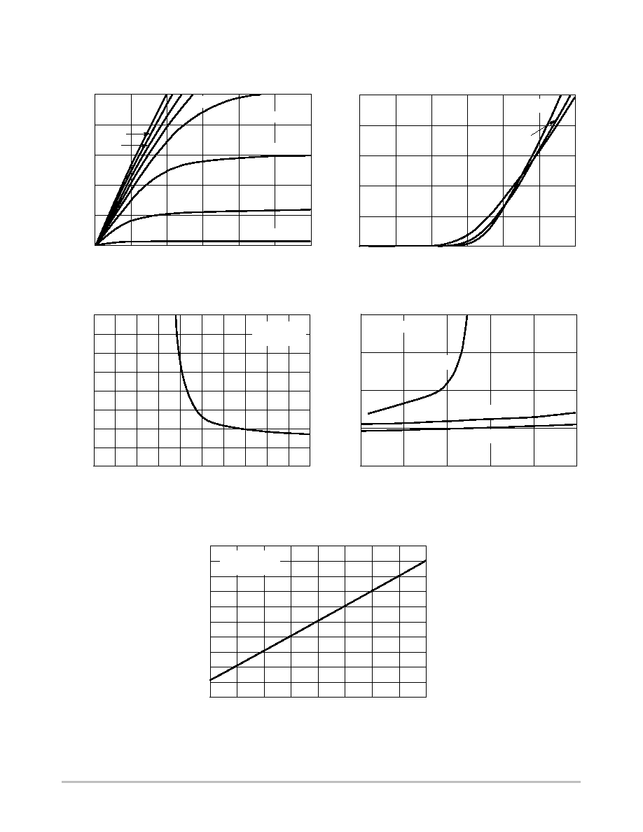
TYPICAL ELECTRICAL CHARACTERISTICS
125
∞
C
-2.5 V
0
20
2.5
16
12
3
1.5
1
-V
DS
, DRAIN-TO-SOURCE VOLTAGE (VOLTS)
-I
D,
DRAIN CURRENT (AMPS)
8
4
0
0.5
Figure 1. On-Region Characteristics
0
20
16
1.5
1
2
12
8
4
0.5
0
2.5
3
Figure 2. Transfer Characteristics
-V
GS
, GATE-TO-SOURCE VOLTAGE (VOLTS)
0
0.05
2
4
0.15
0.1
0
5
Figure 3. On-Resistance versus
Gate-to-Source Voltage
-V
GS
, GATE-TO-SOURCE VOLTAGE (VOLTS)
R
DS(on),
DRAIN-T
O-SOURCE
RESIST
ANCE (
W
)
-I
D,
DRAIN CURRENT (AMPS)
2
18
20
14
10
0.15
0.1
6
0.05
Figure 4. On-Resistance versus Drain Current
and Gate Voltage
-I
D,
DRAIN CURRENT (AMPS)
-50
0
-25
25
1.4
1.2
1
0.8
0.6
50
125
100
Figure 5. On-Resistance Variation with
Temperature
T
J
, JUNCTION TEMPERATURE (
∞
C)
T
J
= 25
∞
C
V
GS
= -1.5 V
0.2
1
3
T
J
= -55
∞
C
I
D
= -3.9 A
T
J
= 25
∞
C
0.2
0
75
150
T
J
= 25
∞
C
V
GS
= 2.5 V
I
D
= -3.9 A
V
GS
= -4.5 V
R
DS(on),
DRAIN-T
O-SOURCE
RESIST
ANCE (NORMALIZED)
2
-2 V
-3 V
-3.5 V
-5 V
-4.5 V
-4 V
25
∞
C
R
DS(on),
DRAIN-T
O-SOURCE
RESIST
ANCE (
W
)
1.6
V
GS
= 3.6 V
V
GS
= 4.5 V
NTHS5441
http://onsemi.com
4
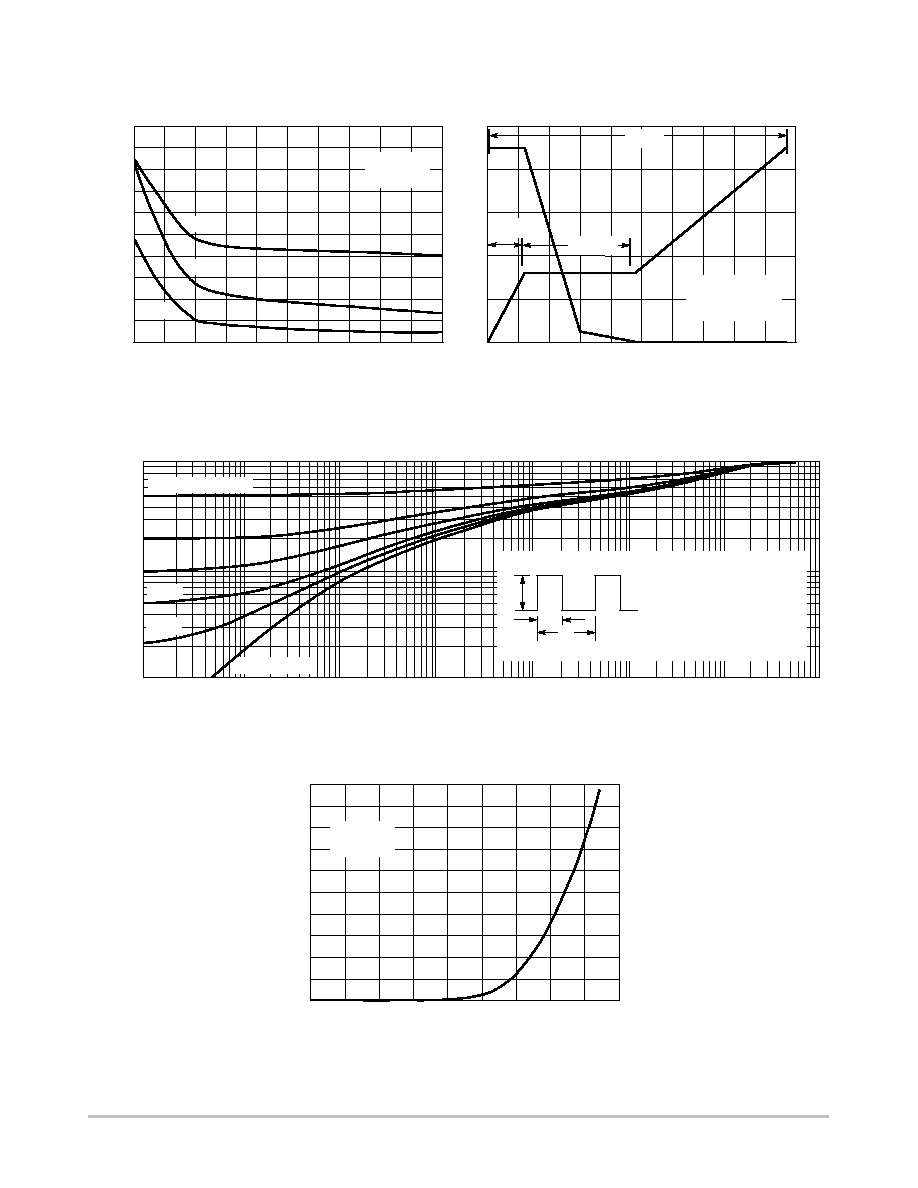
TYPICAL ELECTRICAL CHARACTERISTICS
8
12
4
0
16
1200
900
600
300
0
20
-V
DS
, DRAIN-TO-SOURCE VOLTAGE ()
Figure 6. Capacitance Variation
C, CAP
ACIT
ANCE (pF)
Figure 7. Gate-to-Source and
Drain-to-Source Voltage versus Total Charge
Q
G
, TOTAL GATE CHARGE (nC)
-V
GS
,
GA
TE-T
O-SOURCE
VOL
T
AGE (VOL
TS)
T
J
= 25
∞
C
V
GS
= 0
C
oss
C
iss
C
rss
1500
-V
DS,
DRAIN-T
O-SOURCE
VOL
T
AGE (VOL
TS)
0
1
2
3
4
5
0
1
2
3
4
5
6
7
8
9
10
0
1
2
3
4
5
6
7
8
9
10
11
Q
G
Q
GD
Q
GS
I
D
= -3.9 A
T
J
= 25
∞
C
Q
GD
/Q
GS
= 3.0
0.0001
1
0.01
10
0.1
0.01
SQUARE WAVE PULSE DURATION (sec)
0.1
1
0.001
Figure 8. Normalized Thermal Transient Impedance, Junction-to-Ambient
Duty Cycle = 0.5
100
1000
NORMALIZED EFFECTIVE TRANSIENT
THERMAL IMPEDANCE
0.2
Single Pulse
0.1
0.05
0.02
PER UNIT BASE = R
qJA
= 80∞C/W
T
JM
- T
A
= P
DM
Z
qJA
(t)
SURFACE MOUNTED
P
DM
t
1
t
2
DUTY CYCLE, D = t
1
/t
2
Figure 9. Diode Forward Voltage versus
Current
0.3
0.1
0.5
0.7
0.9
5
3
2
1
0
-I
S
, SOURCE CURRENT (AMPS)
-V
SD
, SOURCE-TO-DRAIN VOLTAGE (VOLTS)
V
GS
= 0 V
T
J
= 25
∞
C
4

NTHS5441
http://onsemi.com
5
PACKAGE DIMENSIONS
ChipFET
]
CASE 1206A-03
ISSUE G
E
A
b
e
e1
D
1
2
3
4
8
7
6
5
c
L
1
2
3
4
8
7
6
5
NOTES:
1. DIMENSIONING AND TOLERANCING PER ANSI Y14.5M, 1982.
2. CONTROLLING DIMENSION: MILLIMETER.
3. MOLD GATE BURRS SHALL NOT EXCEED 0.13 MM PER SIDE.
4. LEADFRAME TO MOLDED BODY OFFSET IN HORIZONTAL
AND VERTICAL SHALL NOT EXCEED 0.08 MM.
5. DIMENSIONS A AND B EXCLUSIVE OF MOLD GATE BURRS.
6. NO MOLD FLASH ALLOWED ON THE TOP AND BOTTOM LEAD
SURFACE.
0.05 (0.002)
DIM
A
MIN
NOM
MAX
MIN
MILLIMETERS
1.00
1.05
1.10
0.039
INCHES
b
0.25
0.30
0.35
0.010
c
0.10
0.15
0.20
0.004
D
2.95
3.05
3.10
0.116
E
1.55
1.65
1.70
0.061
e
0.65 BSC
e1
0.55 BSC
L
0.28
0.35
0.42
0.011
0.041
0.043
0.012
0.014
0.006
0.008
0.120
0.122
0.065
0.067
0.025 BSC
0.022 BSC
0.014
0.017
NOM
MAX
1.80
1.90
2.00
0.071
0.075
0.079
H
E
5
∞ NOM
q
5
∞ NOM
H
E
q
0.457
0.018
2.032
0.08
0.635
0.025
0.66
0.026
0.711
0.028
mm
inches
SCALE 20:1
0.178
0.007
2.032
0.08
1.727
0.068
0.66
0.026
0.711
0.028
mm
inches
SCALE 20:1
Styles 1 and 4
Basic
0.457
0.018
*For additional information on our Pb-Free strategy and soldering
details, please download the ON Semiconductor Soldering and
Mounting Techniques Reference Manual, SOLDERRM/D.
SOLDERING FOOTPRINT*
NTHS5441
http://onsemi.com
6
ON Semiconductor and are registered trademarks of Semiconductor Components Industries, LLC (SCILLC). SCILLC reserves the right to make changes without further notice
to any products herein. SCILLC makes no warranty, representation or guarantee regarding the suitability of its products for any particular purpose, nor does SCILLC assume any liability
arising out of the application or use of any product or circuit, and specifically disclaims any and all liability, including without limitation special, consequential or incidental damages.
"Typical" parameters which may be provided in SCILLC data sheets and/or specifications can and do vary in different applications and actual performance may vary over time. All
operating parameters, including "Typicals" must be validated for each customer application by customer's technical experts. SCILLC does not convey any license under its patent rights
nor the rights of others. SCILLC products are not designed, intended, or authorized for use as components in systems intended for surgical implant into the body, or other applications
intended to support or sustain life, or for any other application in which the failure of the SCILLC product could create a situation where personal injury or death may occur. Should
Buyer purchase or use SCILLC products for any such unintended or unauthorized application, Buyer shall indemnify and hold SCILLC and its officers, employees, subsidiaries, affiliates,
and distributors harmless against all claims, costs, damages, and expenses, and reasonable attorney fees arising out of, directly or indirectly, any claim of personal injury or death
associated with such unintended or unauthorized use, even if such claim alleges that SCILLC was negligent regarding the design or manufacture of the part. SCILLC is an Equal
Opportunity/Affirmative Action Employer. This literature is subject to all applicable copyright laws and is not for resale in any manner.
PUBLICATION ORDERING INFORMATION
N. American Technical Support: 800-282-9855 Toll Free
USA/Canada
Japan: ON Semiconductor, Japan Customer Focus Center
2-9-1 Kamimeguro, Meguro-ku, Tokyo, Japan 153-0051
Phone: 81-3-5773-3850
NTHS5441T1/D
ChipFET is a trademark of Vishay Siliconix.
LITERATURE FULFILLMENT:
Literature Distribution Center for ON Semiconductor
P.O. Box 61312, Phoenix, Arizona 85082-1312 USA
Phone: 480-829-7710 or 800-344-3860 Toll Free USA/Canada
Fax: 480-829-7709 or 800-344-3867 Toll Free USA/Canada
Email: orderlit@onsemi.com
ON Semiconductor Website: http://onsemi.com
Order Literature: http://www.onsemi.com/litorder
For additional information, please contact your
local Sales Representative.