
©
Semiconductor Components Industries, LLC, 2003
November, 2003 - Rev. 1
1
Publication Order Number:
NTMS4404N/D
NTMS4404N
Power MOSFET
30 V, 12 A, Single N-Channel, SO-8
Features
∑
High Density Power MOSFET with Ultra Low R
DS(on)
for Higher
Efficiency
∑
Miniature SO-8 Surface Mount Package Saving Board Space
∑
I
DSS
Specified at Elevated Temperature
∑
Diode Exhibits High Speed, Soft Recovery
Applications
∑
Power Management for Battery Power Products
∑
Portable Products
∑
Computers, Printers, PCMCIA Cards
∑
Cell Phones, Cordless Telephones
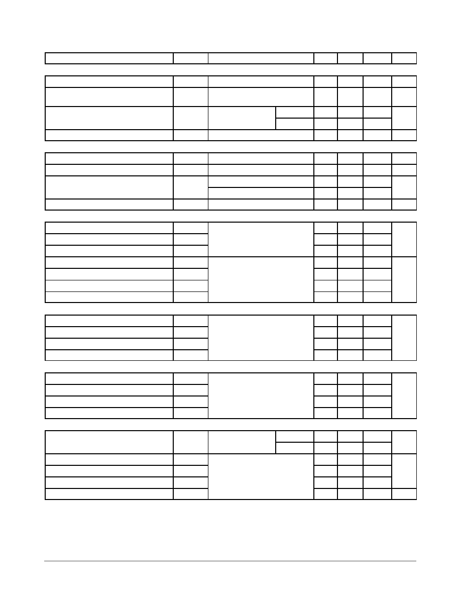
MAXIMUM RATINGS
(T
J
= 25
∞
C unless otherwise stated)
Parameter
Symbol
Value
Unit
Drain-to-Source Voltage
V
DSS
30
V
Gate-to-Source Voltage
V
GS
$
20
V
Continuous Drain
Current (Note 1)
Steady
State
T
A
= 25
∞
C
I
D
9.6
A
Current (Note 1)
State
T
A
= 70
∞
C
7.6
tp
v
10 s
T
A
= 25
∞
C
12
Power Dissipation
(Note 1)
Steady State
P
D
1.56
W
(Note 1)
tp
v
10 s
2.5
Continuous Drain
Current (Note 2)
Steady
State
T
A
= 25
∞
C
I
D
7.0
A
Current (Note 2)
State
T
A
= 70
∞
C
5.6
Power Dissipation
(Note 2)
T
A
= 25
∞
C
P
D
0.83
W
Pulsed Drain Current
tp = 10
m
s, DC = 2 %
I
DM
50
A
Operating Junction and Storage Temperature
T
J
,
T
STG
-55 to
150
∞
C
Source Current (Body Diode)
I
S
6.0
A
Single Pulse Drain-to-Source Avalanche
Energy (V
DD
= 20 V, V
GS
= 5 V, I
PK
= 7.25 A,
L = 19 mH, R
G
= 25
W
)
E
AS
500
mJ
Lead Temperature for Soldering Purposes
(1/8" from case for 10 s)
T
L
260
∞
C
THERMAL RESISTANCE RATINGS
Parameter
Symbol
Max
Unit
Junction-to-Ambient ≠ Steady State (Note 1)
R
q
JA
80
∞
C/W
Junction-to-Ambient ≠ t = 1 0 s (Note 1)
R
q
JA
50
Junction-to-Ambient ≠ Steady State (Note 2)
R
q
JA
150
1. Surface-mounted on FR4 board using 1 in sq. pad size
(Cu area = 1.127 in sq. [1 oz] including traces)
2. Surface-mounted on FR4 board using the minimum recommended pad
size (Cu area = 0.412 in sq.)
G
D
S
Device
Package
Shipping
ORDERING INFORMATION
NTMS4404NR2
SO-8
2500/Tape & Reel
http://onsemi.com
30 V
15.5 m
W
@ 4.5 V
9.7 m
W
@ 10 V
R
DS(on)
TYP
12 A
I
D
MAX
V
(BR)DSS
SO-8
CASE 751
STYLE 12
MARKING DIAGRAM/
PIN ASSIGNMENT
1
E4404N
L
YWW
E4404N = Device Code
L
= Assembly Location
Y
= Year
WW
= Work Week
1
8
Drain
Drain
Drain
Drain
Source
Source
Source
Gate
Top View
N-Channel
For information on tape and reel specifications,
including part orientation and tape sizes, please
refer to our Tape and Reel Packaging Specification
Brochure, BRD8011/D.
NTMS4404N
http://onsemi.com
2
ELECTRICAL CHARACTERISTICS
(T
J
= 25
∞
C unless otherwise specified)
Parameter
Symbol
Test Condition
Min
Typ
Max
Units
OFF CHARACTERISTICS
Drain-to-Source Breakdown Voltage
V
(BR)DSS
V
GS
= 0 V, I
D
= 250
m
A
30
V
Drain-to-Source Breakdown Voltage
Temperature Coefficient
V
(BR)DSS
/
T
J
25
mV/
∞
C
Zero Gate Voltage Drain Current
I
DSS
V
0 V V
30 V
T
J
= 25
∞
C
1.0
m
A
V
GS
= 0 V, V
DS
= 30 V
T
J
= 100
∞
C
5.0
Gate-to-Source Leakage Current
I
GSS
V
DS
= 0 V, V
GS
=
$
20 V
$
100
nA
ON CHARACTERISTICS (Note 3)
Gate Threshold Voltage
V
GS(TH)
V
GS
= V
DS
, I
D
= 250
m
A
1.0
2.2
3.0
V
Gate Threshold Temperature Coefficient
V
GS(TH)
/T
J
-5.0
mV/
∞
C
Drain-to-Source On Resistance
R
DS(on)
V
GS
= 10 V, I
D
= 12 A
9.7
11.5
m
W
(
)
V
GS
= 4.5 V, I
D
= 6.0 A
15.5
17.5
Forward Transconductance
g
FS
V
DS
= 15 V, I
D
= 12 A
17.5
S
CHARGES AND CAPACITANCES
Input Capacitance
C
ISS
1975
2500
pF
Output Capacitance
C
OSS
V
GS
= 0 V, f = 1 MHz, V
DS
= 24 V
575
750
Reverse Transfer Capacitance
C
RSS
GS
,
,
DS
180
300
Total Gate Charge
Q
G(TOT)
50
70
nC
Threshold Gate Charge
Q
G(TH)
V
= 10 V V
= 24 V I = 12 A
2.4
Gate-to-Source Charge
Q
GS
V
GS
= 10 V, V
DS
= 24 V, I
D
= 12 A
7.5
Gate-to-Drain Charge
Q
GD
16
SWITCHING CHARACTERISTICS, V
GS
= 10 V (Note 4)
Turn-On Delay Time
t
d(ON)
15
25
ns
Rise Time
tr
V
GS
= 10 V, V
DS
= 24 V, I
D
= 12 A,
25
50
Turn-Off Delay Time
t
d(OFF)
V
GS
= 10 V, V
DS
= 24 V, I
D
= 12 A,
R
G
= 2.5
W
35
55
Fall Time
t
f
15
30
SWITCHING CHARACTERISTICS, V
GS
= 4.5 V (Note 4)
Turn-On Delay Time
t
d(ON)
20
ns
Rise Time
tr
V
GS
= 4.5 V, V
DS
= 24 V, I
D
= 6.0 A,
80
Turn-Off Delay Time
t
d(OFF)
V
GS
= 4.5 V, V
DS
= 24 V, I
D
= 6.0 A,
R
G
= 2.5
W
25
Fall Time
t
f
15
DRAIN-SOURCE DIODE CHARACTERISTICS (Note 4)
Forward Diode Voltage
V
SD
V
= 0 V I = 6 0 A
T
J
= 25
∞
C
0.80
1.1
V
V
GS
= 0 V, I
S
= 6.0 A
T
J
= 125
∞
C
0.65
Reverse Recovery Time
t
RR
40
55
ns
Charge Time
t
a
V
GS
= 0 V, d
ISD
/d
t
= 100 A/
m
s,
23
Discharge Time
tb
V
GS
0 V, d
ISD
/d
t
100 A/
m
s,
I
S
= 6.0
A
17
Reverse Recovery Charge
Q
RR
0.05
m
C
NOTES:
3. Pulse Test: pulse width
v
300
m
s, duty cycle
v
2%.
4. Switching characteristics are independent of operating junction temperatures.
NTMS4404N
http://onsemi.com
3
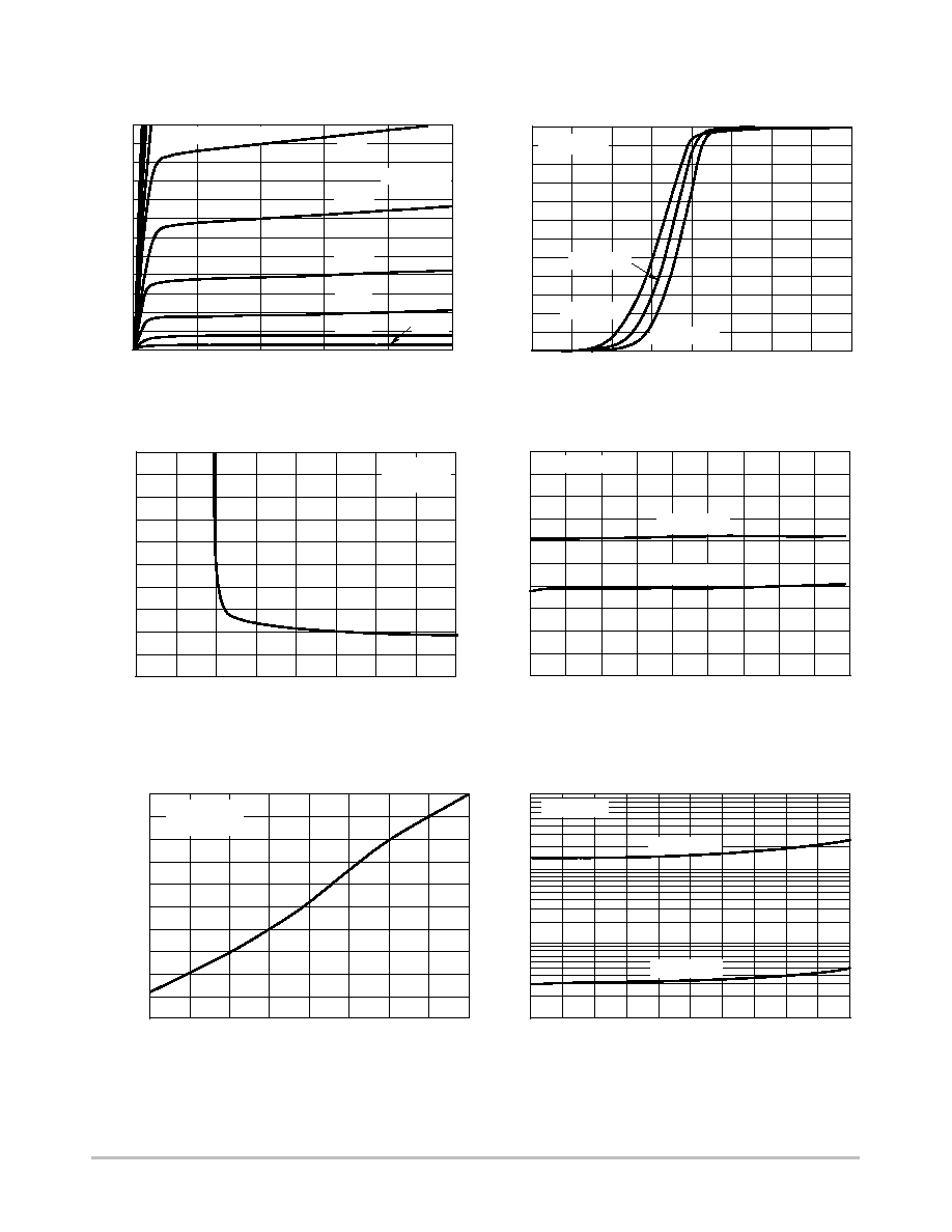
TYPICAL PERFORMANCE CURVES
T
J
= 100
∞
C
0
16
6
2
V
DS
, DRAIN-TO-SOURCE VOLTAGE (VOLTS)
I
D,
DRAIN CURRENT (AMPS)
12
4
0
Figure 1. On-Region Characteristics
2
3
16
12
4
6
0
Figure 2. Transfer Characteristics
V
GS
, GATE-TO-SOURCE VOLTAGE (VOLTS)
0.01
4
6
0.02
0
Figure 3. On-Resistance vs. Gate-to-Source
Voltage
V
GS
, GATE-TO-SOURCE VOLTAGE (VOLTS)
R
DS(on),
DRAIN-T
O-SOURCE
RESIST
ANCE (
W
)
I
D,
DRAIN CURRENT (AMPS)
14
24
0.01
Figure 4. On-Resistance vs. Drain Current and
Gate Voltage
I
D,
DRAIN CURRENT (AMPS)
-50
0
-25
25
1.4
1.2
1
0.8
0.6
50
150
Figure 5. On-Resistance Variation with
Temperature
T
J
, JUNCTION TEMPERATURE (
∞
C)
T
J
= 25
∞
C
0.05
3
5
T
J
= -55
∞
C
I
D
= 12 A
T
J
= 25
∞
C
0.025
0
75
T
J
= 25
∞
C
I
D
= 12 A
V
GS
= 10 V
R
DS(on),
DRAIN-T
O-SOURCE
RESIST
ANCE (NORMALIZED)
4
T
J
= 25
∞
C
R
DS(on),
DRAIN-T
O-SOURCE
RESIST
ANCE (
W
)
1.6
V
GS
= 10 V
2
10
10
25
Figure 6. Drain-to-Source Leakage Current
vs. Voltage
V
DS
, DRAIN-TO-SOURCE VOLTAGE (VOLTS)
15
V
GS
= 0 V
I
DSS
, LEAKAGE (A)
T
J
= 150
∞
C
T
J
= 100
∞
C
3.0 V
3.2 V
0.02
V
GS
= 4.5 V
100
1000
10000
10
4 V
V
DS
10 V
0.04
16
18
20
0.015
10
20
3.8 V
8
3.4 V
8
4
7
9
8
6
8
10
12
30
24
20
3.6 V
V
GS
= 10 V to 4.2 V
20
24
0.03
22
0.005
125
100
5
8
5
NTMS4404N
http://onsemi.com
4
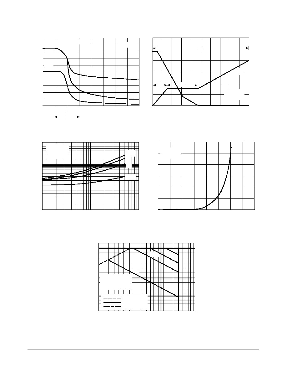
TYPICAL PERFORMANCE CURVES
Figure 7. Capacitance Variation
Figure 8. Gate-To-Source and
Drain-To-Source Voltage vs. Total Charge
0.9
2
0
V
SD
, SOURCE-TO-DRAIN VOLTAGE (VOLTS)
Figure 9. Resistive Switching Time
Variation vs. Gate Resistance
I
S
, SOURCE CURRENT (AMPS)
V
GS
= 0 V
T
J
= 25
∞
C
12
0.7
0.5
10
Figure 10. Diode Forward Voltage vs. Current
0.8
0.6
8
6
Figure 11. Maximum Rated Forward Biased
Safe Operating Area
0.1
V
DS
, DRAIN-TO-SOURCE VOLTAGE (VOLTS)
0.1
1
I D
, DRAIN CURRENT
(AMPS)
R
DS(on)
LIMIT
THERMAL LIMIT
PACKAGE LIMIT
V
GS
= 10 V
SINGLE PULSE
T
C
= 25
∞
C
10
0.01
dc
1
100
100
10
10 ms
1 ms
100 ms
GATE-TO-SOURCE OR DRAIN-TO-SOURCE VOLTAGE (VOLTS)
C, CAP
ACIT
ANCE (pF)
1000
5000
30
10
0
5
10
5
T
J
= 25
∞
C
C
iss
C
oss
C
rss
15
20
25
0
2000
3000
C
iss
C
rss
V
DS
= 0 V
V
GS
= 0 V
V
DS
V
GS
30
V
GS
, GA
TE-T
O-SOURCE VOL
T
AGE (VOL
TS)
10
20
0
0
5
0
Q
G
, TOTAL GATE CHARGE (nC)
VDS
, DRAIN-T
O-SOURCE VOL
T
AGE (VOL
TS)
15
10
10
20
40
I
D
= 12 A
T
J
= 25
∞
C
30
V
DS
V
GS
Q
GS
50
R
G
, GATE RESISTANCE (OHMS)
1
10
100
100
10
t, TIME
(ns)
V
DD
= 24 V
I
D
= 12 A
V
GS
= 10 V
t
r
t
d(on)
1000
t
f
t
d(off)
Q
GD
QT
1
4
4000
NTMS4404N
http://onsemi.com
5
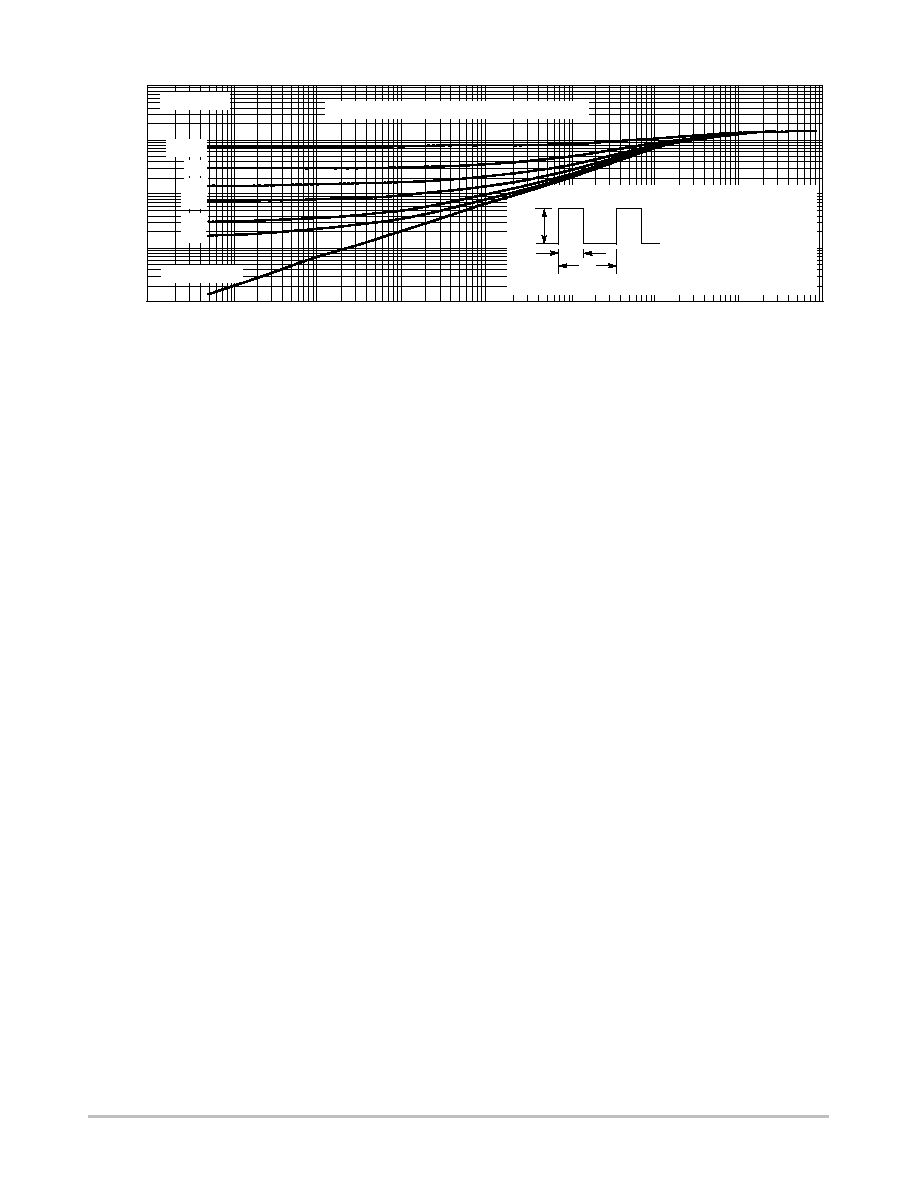
Figure 12. Thermal Response - Various Duty Cycles
t, TIME (seconds)
Rthja(t)
, EFFECTIVE
TRANSIENT
THERMAL
RESIST
ANCE
1000
10
1
D = 0.5
SINGLE PULSE
1E-05
1E-04
1E-03
1E-02
1E-01
0.2
0.01
1E+03
0.1
R
JA
(t) = r(t) R
JA
D CURVES APPLY FOR POWER
PULSE TRAIN SHOWN
READ TIME AT t
1
T
J(pk)
- T
A
= P
(pk)
R
JA
(t)
P
(pk)
t
1
t
2
DUTY CYCLE, D = t
1
/t
2
100
0.02
0.05
0.1
1E+00
1E+01
1E+02
DUTY CYCLE
MOUNTED TO MINIMUM RECOMMENDED FOOTPRINT
NTMS4404N
http://onsemi.com
6
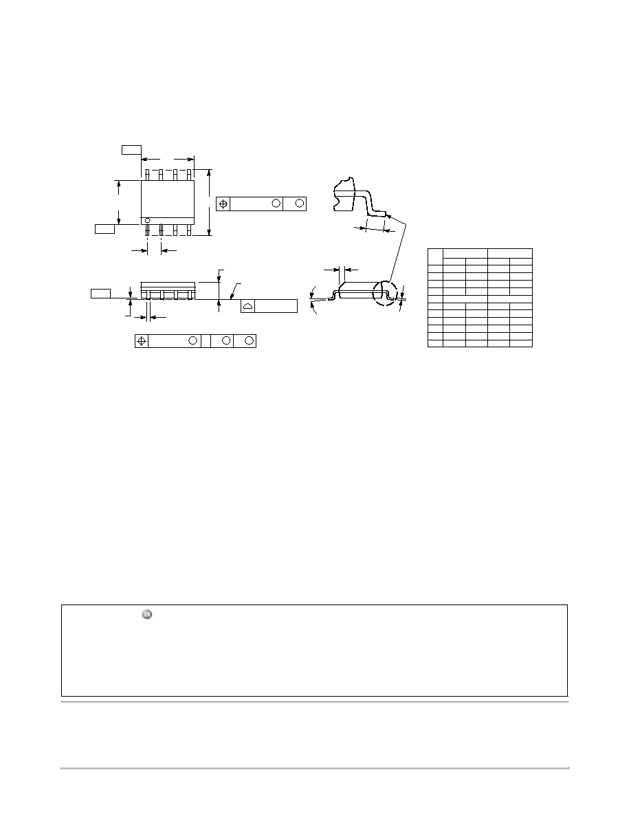
PACKAGE DIMENSIONS
SOIC-8 NB
CASE 751-07
ISSUE AA
SEATING
PLANE
1
4
5
8
N
J
X 45
_
K
NOTES:
1. DIMENSIONING AND TOLERANCING PER ANSI
Y14.5M, 1982.
2. CONTROLLING DIMENSION: MILLIMETER.
3. DIMENSION A AND B DO NOT INCLUDE MOLD
PROTRUSION.
4. MAXIMUM MOLD PROTRUSION 0.15 (0.006) PER
SIDE.
5. DIMENSION D DOES NOT INCLUDE DAMBAR
PROTRUSION. ALLOWABLE DAMBAR
PROTRUSION SHALL BE 0.127 (0.005) TOTAL IN
EXCESS OF THE D DIMENSION AT MAXIMUM
MATERIAL CONDITION.
6. 751-01 THRU 751-06 ARE OBSOLETE. NEW
STANDARD IS 751-07.
A
B
S
D
H
C
0.10 (0.004)
DIM
A
MIN
MAX
MIN
MAX
INCHES
4.80
5.00
0.189
0.197
MILLIMETERS
B
3.80
4.00
0.150
0.157
C
1.35
1.75
0.053
0.069
D
0.33
0.51
0.013
0.020
G
1.27 BSC
0.050 BSC
H
0.10
0.25
0.004
0.010
J
0.19
0.25
0.007
0.010
K
0.40
1.27
0.016
0.050
M
0
8
0
8
N
0.25
0.50
0.010
0.020
S
5.80
6.20
0.228
0.244
-X-
-Y-
G
M
Y
M
0.25 (0.010)
-Z-
Y
M
0.25 (0.010)
Z
S
X
S
M
_
_
_
_
STYLE 12:
PIN 1. SOURCE
2. SOURCE
3. SOURCE
4. GATE
5. DRAIN
6. DRAIN
7. DRAIN
8. DRAIN
ON Semiconductor and are registered trademarks of Semiconductor Components Industries, LLC (SCILLC). SCILLC reserves the right to make changes without further notice
to any products herein. SCILLC makes no warranty, representation or guarantee regarding the suitability of its products for any particular purpose, nor does SCILLC assume any liability
arising out of the application or use of any product or circuit, and specifically disclaims any and all liability, including without limitation special, consequential or incidental damages.
"Typical" parameters which may be provided in SCILLC data sheets and/or specifications can and do vary in different applications and actual performance may vary over time. All
operating parameters, including "Typicals" must be validated for each customer application by customer's technical experts. SCILLC does not convey any license under its patent rights
nor the rights of others. SCILLC products are not designed, intended, or authorized for use as components in systems intended for surgical implant into the body, or other applications
intended to support or sustain life, or for any other application in which the failure of the SCILLC product could create a situation where personal injury or death may occur. Should
Buyer purchase or use SCILLC products for any such unintended or unauthorized application, Buyer shall indemnify and hold SCILLC and its officers, employees, subsidiaries, affiliates,
and distributors harmless against all claims, costs, damages, and expenses, and reasonable attorney fees arising out of, directly or indirectly, any claim of personal injury or death
associated with such unintended or unauthorized use, even if such claim alleges that SCILLC was negligent regarding the design or manufacture of the part. SCILLC is an Equal
Opportunity/Affirmative Action Employer. This literature is subject to all applicable copyright laws and is not for resale in any manner.
PUBLICATION ORDERING INFORMATION
N. American Technical Support: 800-282-9855 Toll Free
USA/Canada
Japan: ON Semiconductor, Japan Customer Focus Center
2-9-1 Kamimeguro, Meguro-ku, Tokyo, Japan 153-0051
Phone: 81-3-5773-3850
NTMS4404N/D
LITERATURE FULFILLMENT:
Literature Distribution Center for ON Semiconductor
P.O. Box 5163, Denver, Colorado 80217 USA
Phone: 303-675-2175 or 800-344-3860 Toll Free USA/Canada
Fax: 303-675-2176 or 800-344-3867 Toll Free USA/Canada
Email: orderlit@onsemi.com
ON Semiconductor Website: http://onsemi.com
Order Literature: http://www.onsemi.com/litorder
For additional information, please contact your
local Sales Representative.