Äîêóìåíòàöèÿ è îïèñàíèÿ www.docs.chipfind.ru
©
Semiconductor Components Industries, LLC, 2004
December, 2004 - Rev. 7
1
Publication Order Number:
NUD3105/D
NUD3105
Integrated Relay,
Inductive Load Driver
This device is used to switch inductive loads such as relays,
solenoids incandescent lamps , and small DC motors without the need
of a free-wheeling diode. The device integrates all necessary items
such as the MOSFET switch, ESD protection, and Zener clamps. It
accepts logic level inputs thus allowing it to be driven by a large
variety of devices including logic gates, inverters, and
microcontrollers.
Features
·
Provides a Robust Driver Interface Between DC Relay Coil and
Sensitive Logic Circuits
·
Optimized to Switch Relays from 3.0 V to 5.0 V Rail
·
Capable of Driving Relay Coils Rated up to 2.5 W at 5.0 V
·
Internal Zener Eliminates the Need of Free-Wheeling Diode
·
Internal Zener Clamp Routes Induced Current to Ground for Quieter
Systems Operation
·
Low V
DS(ON)
Reduces System Current Drain
·
Pb-Free Package is Available
Typical Applications
·
Telecom: Line Cards, Modems, Answering Machines, FAX
·
Computers and Office: Photocopiers, Printers, Desktop Computers
·
Consumer: TVs and VCRs, Stereo Receivers, CD Players,
Cassette Recorders
·
Industrial:Small Appliances, Security Systems, Automated
Test Equipment, Garage Door Openers
·
Automotive: 5.0 V Driven Relays, Motor Controls, Power
Latches, Lamp Drivers
Device
Package
Shipping
ORDERING INFORMATION
NUD3105LT1
SOT-23
3000 Units/Reel
MARKING
DIAGRAM
1
2
3
SOT-23
TO-236
CASE 318
INTERNAL CIRCUIT DIAGRAM
Drain (3)
1.0 k
300 k
Gate (1)
Source (2)
JW4D
JW4
= Specific Device Code
D
= Date Code
For information on tape and reel specifications,
including part orientation and tape sizes, please
refer to our Tape and Reel Packaging Specification
Brochure, BRD8011/D.
RELAY/INDUCTIVE
LOAD DRIVER
SILICON SMALLBLOCK
t
0.5 Ampere, 8.0 V Clamp
NUD3105LT1G
SOT-23
(Pb-Free)
3000 Units/Reel
http://onsemi.com
NUD3105
http://onsemi.com
2
MAXIMUM RATINGS (T
J
= 25
°
C unless otherwise specified)
Symbol
Rating
Value
Unit
V
DSS
Drain to Source Voltage - Continuous
6.0
V
dc
V
GS
Gate to Source Voltage Continuous
6.0
V
dc
I
D
Drain Current Continuous
500
mA
E
z
Single Pulse Drain-to-Source Avalanche Energy (
T
Jinitial =
25
°
C) (Note 2)
50
mJ
E
zpk
Repetitive Pulse Zener Energy Limit (DC
v
0.01%) (f = 100 Hz, DC = 0.5)
4.5
mJ
T
J
Junction Temperature
150
°
C
T
A
Operating Ambient Temperature
-40 to 85
°
C
T
stg
Storage Temperature Range
-65 to +150
°
C
P
D
Total Power Dissipation (Note 1)
Derating Above 25
°
C
225
1.8
mW
mW/
°
C
R
q
JA
Thermal Resistance Junction-to-Ambient
556
°
C/W
Maximum ratings are those values beyond which device damage can occur. Maximum ratings applied to the device are individual stress limit
values (not normal operating conditions) and are not valid simultaneously. If these limits are exceeded, device functional operation is not implied,
damage may occur and reliability may be affected.
1. This device contains ESD protection and exceeds the following tests:
Human Body Model 2000 V per MIL_STD-883, Method 3015.
Machine Model Method 200 V.
2. Refer to the section covering Avalanche and Energy.
TYPICAL ELECTRICAL CHARACTERISTICS (T
J
= 25
°
C unless otherwise noted)
Symbol
Characteristic
Min
Typ
Max
Unit
OFF CHARACTERISTICS
V
BRDSS
Drain to Source Sustaining Voltage (Internally Clamped)
(ID = 10 mA)
6.0
8.0
9.0
V
B
VGSO
I
g
= 1.0 mA
-
-
8.0
V
I
DSS
Drain to Source Leakage Current
(V
DS
= 5.5 V , V
GS
= 0 V, T
J
= 25
°
C)
(V
DS
= 5.5 V, V
GS
= 0 V, T
J
= 85
°
C )
-
-
-
-
15
15
m
A
I
GSS
Gate Body Leakage Current
(V
GS
= 3.0 V, V
DS
= 0 V)
(V
GS
= 5.0 V, V
DS
= 0 V)
5.0
-
-
-
19
50
m
A
ON CHARACTERISTICS
V
GS(th)
Gate Threshold Voltage
(V
GS
= V
DS
, I
D
= 1.0 mA)
(V
GS
= V
DS
, I
D
= 1.0 mA, T
J
= 85
°
C)
0.8
0.8
1.2
-
1.4
1.4
V
R
DS(on)
Drain to Source On-Resistance
(I
D
= 250 mA, V
GS
= 3.0 V)
(I
D
= 500 mA, V
GS
= 3.0 V)
(I
D
= 500 mA, V
GS
= 5.0 V)
(I
D
= 500 mA, V
GS
= 3.0 V, T
J
=85
°
C)
(I
D
= 500 mA, V
GS
= 5.0 V, T
J
=85
°
C)
-
-
-
-
-
-
-
-
-
-
1.2
1.3
0.9
1.3
0.9
W
I
DS(on)
Output Continuous Current
(V
DS
= 0.25 V, V
GS
= 3.0 V)
(V
DS
= 0.25 V, V
GS
= 3.0 V, T
J
= 85
°
C)
300
200
400
-
-
-
mA
g
FS
Forward Transconductance
(V
OUT
= 5.0 V, I
OUT
= 0.25 A)
350
570
-
mmhos
DYNAMIC CHARACTERISTICS
C
iss
Input Capacitance
(V
DS
= 5.0 V,V
GS
= 0 V, f = 10 kHz)
-
25
-
pF
NUD3105
http://onsemi.com
3
TYPICAL ELECTRICAL CHARACTERISTICS (T
J
= 25
°
C unless otherwise noted)
Symbol
Unit
Max
Typ
Min
Characteristic
DYNAMIC CHARACTERISTICS
C
oss
Output Capacitance
(V
DS
= 5.0 V, V
GS
= 0 V, f = 10 kHz)
-
37
-
pF
C
rss
Transfer Capacitance
(V
DS
= 5.0 V, V
GS
= 0 V, f = 10 kHz)
-
8.0
-
pF
SWITCHING CHARACTERISTICS
Symbol
Characteristic
Min
Typ
Max
Units
t
PHL
t
PLH
t
PHL
t
PLH
Propagation Delay Times:
High to Low Propagation Delay; Figure 1 (5.0 V)
Low to High Propagation Delay; Figure 1 (5.0 V)
High to Low Propagation Delay; Figure 1 (3.0 V)
Low to High Propagation Delay; Figure 1 (3.0 V)
-
-
-
-
25
80
44
44
-
-
-
-
nS
t
f
t
r
t
f
t
r
Transition Times:
Fall Time; Figure 1 (5.0 V)
Rise Time; Figure 1 (5.0 V)
Fall Time; Figure 1 (3.0 V)
Rise Time; Figure 1 (3.0 V)
-
-
-
-
23
32
53
30
-
-
-
-
nS
-
Figure 1. Switching Waveforms
V
out
V
in
0 V
V
OH
V
IH
t
r
t
f
t
PLH
t
PHL
50%
90%
50%
10%
V
OL
NUD3105
http://onsemi.com
4
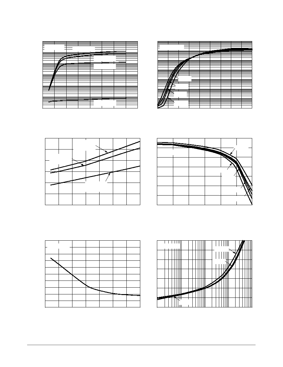
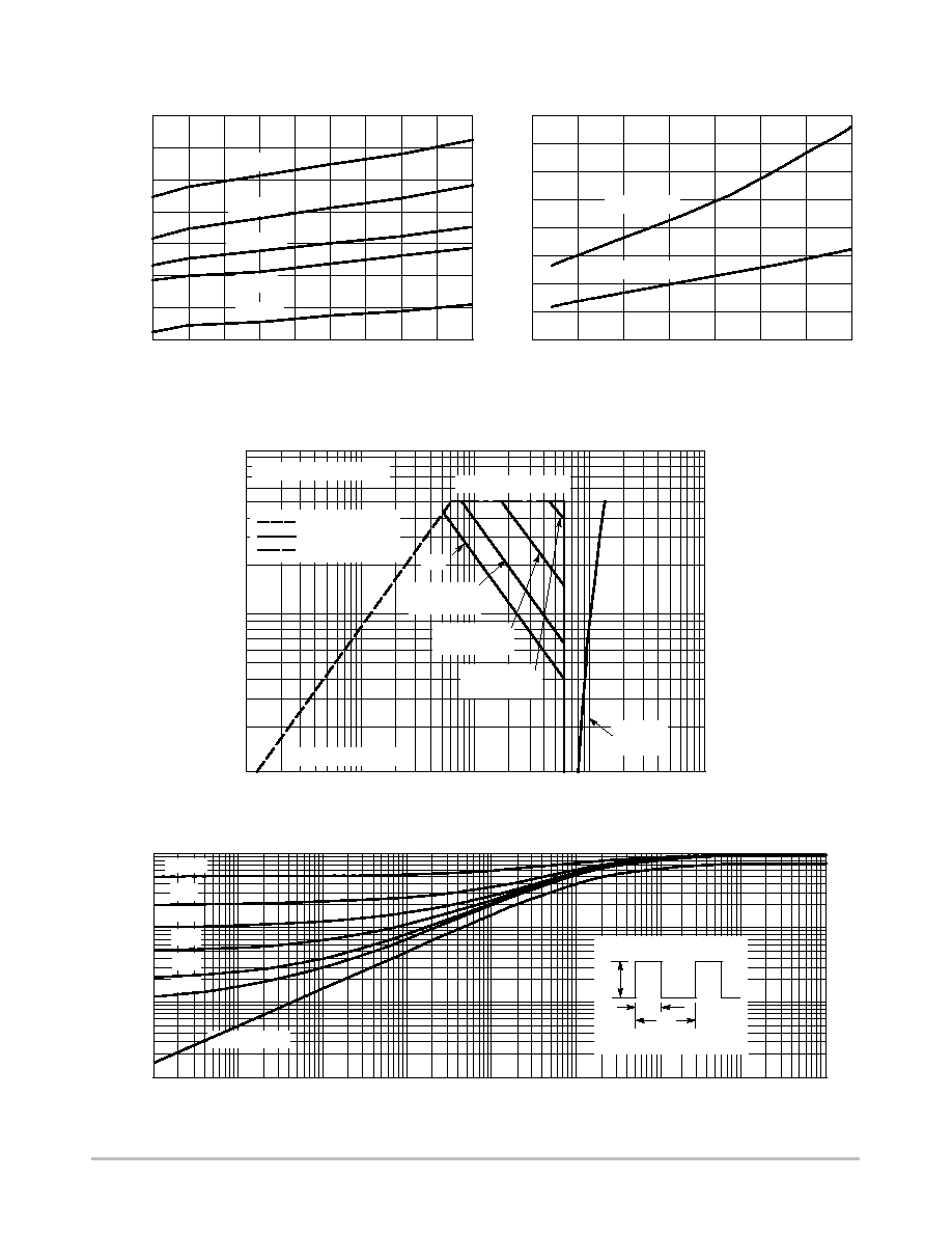
TYPICAL CHARACTERISTICS
V
Z
, ZENER CLAMP VOL
T
AGE (V)
V
GS
= 0 V
11.0
12.0
10.0
9.0
8.0
7.0
13.0
0.1
0.2
0.3
0.4
0.5
0.6
0.7
0.8
0
V
DS
, DRAIN TO SOURCE VOLTAGE (V)
Figure 2. Output Characteristics
V
GS
, GATE-TO-SOURCE VOLTAGE (V)
Figure 3. Transfer Function
TEMPERATURE (
°
C)
Figure 4. On Resistance Variation vs. Temperature
Figure 5. R
DS(ON)
Variation with
Gate-To-Source Voltage
Figure 6. Zener Voltage vs. Temperature
I
Z
, ZENER CURRENT (mA)
Figure 7. Zener Clamp Voltage vs. Zener Current
I
D
, DRAIN CURRENT (A)
-50
-25
0
25
50
75
100
1200
1000
800
600
400
200
0
125
R
DS
(ON)
, DRAIN-T
O-SOURCE
RESIST
ANCE (m
W
)
V
Z
, ZENER VOL
T
AGE (V)
-50
-25
0
25
50
75
100
125
I
Z
= 10 mA
I
D
= 0.25 A
V
GS
= 3.0 V
50
°
C
1.0
1.2
1.4
1.6
0.8
50
45
40
35
30
25
20
2.0
15
1.8
R
DS
(ON)
, DRAIN-T
O-SOURCE
RESIST
ANCE (
W
)
I
D
= 250
m
A
1.0
10
0.1
100
V
GS
= 0 V
V
GS
= 1.0 V
I
D
, DRAIN CURRENT (A)
V
GS
= 5.0 V
V
GS
= 3.0 V
V
GS
= 2.0 V
T
J
= 25
°
C
10
1.0
0.1
0.01
0.001
0.0001
0.00001
0.000001
0.5
1.0
1.5
2.0
2.5
3.0
3.5
4.0
4.5
5.0
85
°
C
-40
°
C
V
DS
= 0.8 V
I
D
= 0.5 A
V
GS
= 3.0 V
I
D
= 0.5 A
V
GS
= 5.0 V
V
GS
, GATE-TO-SOURCE VOLTAGE (V)
50
°
C
85
°
C
-40
°
C
125
°
C
8.20
8.18
8.16
8.14
8.12
8.10
8.08
8.06
8.04
8.02
8.00
TEMPERATURE (
°
C)
10
1.0
0.1
0.01
0.001
0.0001
0.00001
85
°
C
-40
°
C
25
°
C
25
°
C
25
°
C
1000
6.0
NUD3105
http://onsemi.com
5
TYPICAL CHARACTERISTICS
V
DS
, DRAIN-TO-SOURCE VOLTAGE (V)
0.01
100
10
0.1
0.1
1.0
0.01
I
D
, DRAIN CURRENT (A)
1.0
R
DS(on)
LIMIT
THERMAL LIMIT
PACKAGE LIMIT
I
D
, DRAIN CURRENT (A)
Figure 8. On-Resistance vs. Drain Current and
Temperature
TEMPERATURE (
°
C)
Figure 9. Gate Leakage vs. Temperature
R
DS
(ON)
, DRAIN-T
O-SOURCE
RESIST
ANCE (
W
)
1.0
0.9
0.8
0.5
0.6
0.7
1.1
1.2
0.05
0.1
0.15
0.2
0.25
0.3
0.35
0.4
0.45
0.5
I
GS
S
, GA
TE LEAKAGE (
m
A)
30
25
0
5
10
35
40
-50
-25
0
25
50
75
100
125
20
15
125
°
C
85
°
C
50
°
C
25
°
C
-40
°
C
V
GS
= 3.0 V
V
GS
= 5.0 V
Figure 10. Safe Operating Area
Figure 11. Transient Thermal Response
0.01
0.1
1.0
10
100
1000
10,000
100,000
1,000,000
D = 0.5
0.2
0.1
0.05
0.02
SINGLE PULSE
0.01
P
d(pk)
t
1
t
2
DUTY CYCLE = t
1
/t
2
PERIOD
PW
r(t), TRANSIENT
THERMAL
RESIST
ANCE (NORMALIZED)
1.0
0.1
0.01
0.001
t1, PULSE WIDTH (ms)
DC
PW = 0.1 s
DC = 50%
PW = 7.0 ms
DC = 5%
PW = 10 ms
DC = 20%
Typical
I
Z
vs. V
Z
V
(BR)DSS
min = 6.0 V
I
D-Continuous
= 0.5 A
V
GS
= 3.0 V, T
C
= 25
°
C
NUD3105
http://onsemi.com
6
Designing with this Data Sheet
1. Determine the maximum inductive load current (at
max V
CC
, min coil resistance & usually minimum
temperature) that the NUD3105 will have to drive
and make sure it is less than the max rated current.
2. For pulsed operation, use the Transient Thermal
Response of Figure 11 and the instructions with it
to determine the maximum limit on transistor
power dissipation for the desired duty cycle and
temperature range.
3. Use Figures 10 and 11 with the SOA notes to
insure that instantaneous operation does not push
the device beyond the limits of the SOA plot.
4. Verify that the circuit driving the gate will meet
the V
GS(th)
from the Electrical Characteristics
table.
5. Using the max output current calculated in step 1,
check Figure 7 to insure that the range of Zener
clamp voltage over temperature will satisfy all
system & EMI requirements.
6. Use I
GSS
and I
DSS
from the Electrical
Characteristics table to insure that "OFF" state
leakage over temperature and voltage extremes
does not violate any system requirements.
7. Review circuit operation and insure none of the
device max ratings are being exceeded.
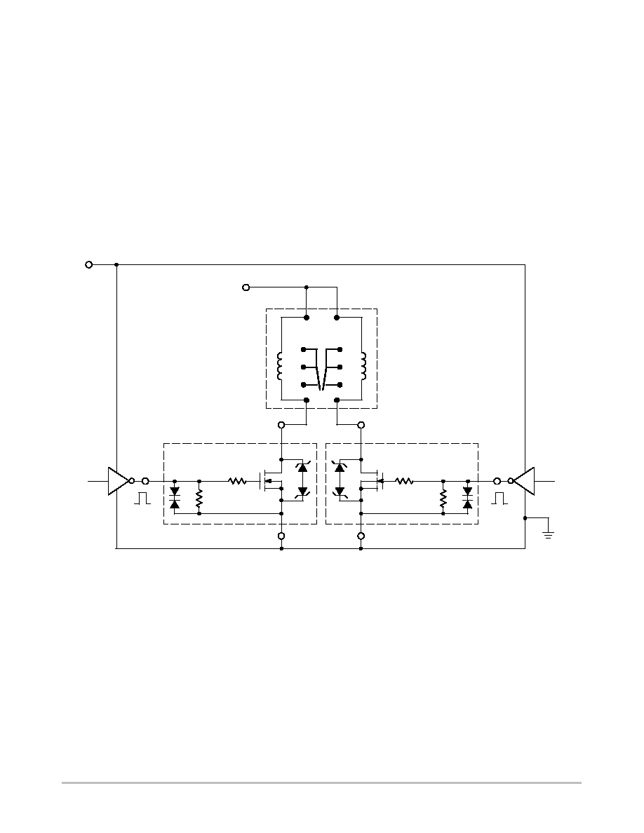
Figure 12. A 200 mW, 5.0 V Dual Coil Latching Relay Application
with 3.0 V Level Translating Interface
+4.5
V
CC
+5.5 Vdc
+
V
out
(3)
+
V
in
(1)
GND (2)
NUD3105LT1
+3.0
V
DD
+3.75 Vdc
APPLICATIONS DIAGRAMS
V
out
(3)
V
in
(1)
GND (2)
NUD3105LT1
NUD3105
http://onsemi.com
7
Figure 13. A 140 mW, 5.0 V Relay with TTL Interface
+4.5 TO +5.5 Vdc
+
V
out
(3)
-
AROMAT
TX2-5V
Max Continuous Current Calculation
for TX2-5V Relay, R1 = 178
W
Nominal @ R
A
= 25
°
C
Assuming
±
10% Make Tolerance,
R1 = 178
W
* 0.9 = 160
W
Min @ T
A
= 25
°
C
T
C
for Annealed Copper Wire is 0.4%/
°
C
R1 = 160
W
* [1+(0.004) * (-40
°
-25
°
)] = 118
W
Min @ -40
°
C
I
O
Max = (5.5 V Max - 0.25V) /118
W
= 45 mA
+
V
out
(3)
-
AROMAT
JS1E-5V
Figure 14. A Quad 5.0 V, 360 mW Coil Relay Bank
-
+
AROMAT
JS1E-5V
+
-
AROMAT
JS1E-5V
-
+
AROMAT
JS1E-5V
+4.5 TO +5.5 Vdc
V
in
(1)
GND (2)
NUD3105LT1
V
in
(1)
GND (2)
NUD3105LT1
NUD3105
http://onsemi.com
8
PACKAGE DIMENSIONS
STYLE 21:
PIN 1. GATE
2. SOURCE
3. DRAIN
D
J
K
L
A
C
B S
H
G
V
3
1
2
SOT-23 (TO-236)
CASE 318-08
ISSUE AK
DIM
A
MIN
MAX
MIN
MAX
MILLIMETERS
0.1102
0.1197
2.80
3.04
INCHES
B
0.0472
0.0551
1.20
1.40
C
0.0350
0.0440
0.89
1.11
D
0.0150
0.0200
0.37
0.50
G
0.0701
0.0807
1.78
2.04
H
0.0005
0.0040
0.013
0.100
J
0.0034
0.0070
0.085
0.177
K
0.0140
0.0285
0.35
0.69
L
0.0350
0.0401
0.89
1.02
S
0.0830
0.1039
2.10
2.64
V
0.0177
0.0236
0.45
0.60
NOTES:
1. DIMENSIONING AND TOLERANCING PER ANSI
Y14.5M, 1982.
2. CONTROLLING DIMENSION: INCH.
3. MAXIMUM LEAD THICKNESS INCLUDES LEAD
FINISH THICKNESS. MINIMUM LEAD
THICKNESS IS THE MINIMUM THICKNESS OF
BASE MATERIAL.
4. 318-03 AND -07 OBSOLETE, NEW STANDARD
318-08.
mm
inches
SCALE 10:1
0.8
0.031
0.9
0.035
0.95
0.037
0.95
0.037
2.0
0.079
*For additional information on our Pb-Free strategy and soldering
details, please download the ON Semiconductor Soldering and
Mounting Techniques Reference Manual, SOLDERRM/D.
SOLDERING FOOTPRINT*
ON Semiconductor and are registered trademarks of Semiconductor Components Industries, LLC (SCILLC). SCILLC reserves the right to make changes without further notice
to any products herein. SCILLC makes no warranty, representation or guarantee regarding the suitability of its products for any particular purpose, nor does SCILLC assume any liability
arising out of the application or use of any product or circuit, and specifically disclaims any and all liability, including without limitation special, consequential or incidental damages.
"Typical" parameters which may be provided in SCILLC data sheets and/or specifications can and do vary in different applications and actual performance may vary over time. All
operating parameters, including "Typicals" must be validated for each customer application by customer's technical experts. SCILLC does not convey any license under its patent rights
nor the rights of others. SCILLC products are not designed, intended, or authorized for use as components in systems intended for surgical implant into the body, or other applications
intended to support or sustain life, or for any other application in which the failure of the SCILLC product could create a situation where personal injury or death may occur. Should
Buyer purchase or use SCILLC products for any such unintended or unauthorized application, Buyer shall indemnify and hold SCILLC and its officers, employees, subsidiaries, affiliates,
and distributors harmless against all claims, costs, damages, and expenses, and reasonable attorney fees arising out of, directly or indirectly, any claim of personal injury or death
associated with such unintended or unauthorized use, even if such claim alleges that SCILLC was negligent regarding the design or manufacture of the part. SCILLC is an Equal
Opportunity/Affirmative Action Employer. This literature is subject to all applicable copyright laws and is not for resale in any manner.
PUBLICATION ORDERING INFORMATION
N. American Technical Support: 800-282-9855 Toll Free
USA/Canada
Japan: ON Semiconductor, Japan Customer Focus Center
2-9-1 Kamimeguro, Meguro-ku, Tokyo, Japan 153-0051
Phone: 81-3-5773-3850
NUD3105/D
SMALLBLOCK is a trademark of Semiconductor Components Industries, LLC (SCILLC).
LITERATURE FULFILLMENT:
Literature Distribution Center for ON Semiconductor
P.O. Box 61312, Phoenix, Arizona 85082-1312 USA
Phone: 480-829-7710 or 800-344-3860 Toll Free USA/Canada
Fax: 480-829-7709 or 800-344-3867 Toll Free USA/Canada
Email: orderlit@onsemi.com
ON Semiconductor Website: http://onsemi.com
Order Literature: http://www.onsemi.com/litorder
For additional information, please contact your
local Sales Representative.