 | –≠–ª–µ–∫—Ç—Ä–æ–Ω–Ω—ã–π –∫–æ–º–ø–æ–Ω–µ–Ω—Ç: AOP604 | –°–∫–∞—á–∞—Ç—å:  PDF PDF  ZIP ZIP |

Symbol
Max p-channel
Units
V
DS
V
V
GS
V
I
DM
T
J
, T
STG
∞C
Symbol
V
DS
I
DM
T
J
, T
STG
-30
±20
Gate-Source Voltage
A
Continuous Drain
Current
A
T
A
=25∞C
I
D
T
A
=70∞C
Pulsed Drain Current
B
W
7.5
6
30
2.5
1.6
-5.3
-6.6
2.5
1.6
Absolute Maximum Ratings T
A
=25∞C unless otherwise noted
Parameter
Max n-channel
30
-30
±20
Drain-Source Voltage
T
A
=70∞C
Power Dissipation
T
A
=25∞C
P
D
Units
V
Junction and Storage Temperature Range
-55 to 150
-55 to 150
Parameter
Maximum Schottky
Reverse Voltage
30
A
T
A
=70∞C
2.7
Pulsed Forward Current
B
20
Continuous Forward
Current
A
T
A
=25∞C
I
D
4
W
T
A
=70∞C
1.6
Junction and Storage Temperature Range
-55 to 150
∞C
Power Dissipation
A
T
A
=25∞C
P
D
2.5
AOP604
Complementary Enhancement Mode Field Effect Transistor
March 2003
Features
n-channel p-channel
V
DS
(V) = 30V -30V
I
D
= 7.5A -6.6A
R
DS(ON)
< 28m
< 35m (V
GS
= 10V)
< 43m
< 58m (V
GS
= 4.5V)
Schottky
V
DS
=30V, I
F
=3A, V
F
<0.5V@1A
General Description
The AOP604 uses advanced trench technology to
provide excellent R
DS(ON)
and low gate charge. The
complementary MOSFETs form a high-speed power
inverter, suitable for a multitude of applications. A
Schottky diode in parallel with the n-channel FET
reduces body diode related losses.
D2
G2
S2
G1
D1
S1
K
A
G1
S1/A
G2
S2
D1/K
D1/K
D2
D2
1
2
3
4
8
7
6
5
N-ch
P-ch
PDIP-8
Alpha & Omega Semiconductor, Ltd.

AOP60
4
Symbol
Typ
Max
40
50
67
80
R
JL
33
40
Symbol
Typ
Max
38
50
66
80
R
JL
30
40
Symbol
Typ
Max
42
50
70
80
R
JL
34
40
Maximum Junction-to-Lead
C
Steady-State
∞C/W
Parameter
Units
Maximum Junction-to-Ambient
A
t 10s
R
JA
∞C/W
Maximum Junction-to-Ambient
A
Steady-State
∞C/W
Maximum Junction-to-Lead
C
Steady-State
∞C/W
Thermal Characteristics: Schottky
Parameter
Units
Maximum Junction-to-Ambient
A
t 10s
R
JA
∞C/W
Maximum Junction-to-Ambient
A
Steady-State
∞C/W
Thermal Characteristics: n-channel
Thermal Characteristics: p-channel
Maximum Junction-to-Lead
C
Steady-State
∞C/W
Parameter
Units
Maximum Junction-to-Ambient
A
t 10s
R
JA
∞C/W
Maximum Junction-to-Ambient
A
Steady-State
∞C/W
A: The value of R
JA
is measured with the device mounted on 1in
2
FR-4 board with 2oz. Copper, in a still air environment with T
A
=25∞C. The
value in any a given application depends on the user's specific board design. The current rating is based on the t 10s thermal resistance
rating.
B: Repetitive rating, pulse width limited by junction temperature.
C. The R
JA
is the sum of the thermal impedence from junction to lead R
JL
and lead to ambient.
D. The static characteristics in Figures 1 to 6 are obtained using 80
µs pulses, duty cycle 0.5% max.
E. These tests are performed with the device mounted on 1 in
2
FR-4 board with 2oz. Copper, in a still air environment with T
A
=25∞C. The
SOA curve provides a single pulse rating.
Alpha Omega Semiconductor, Ltd.

AOP604
Symbol
Min
Typ
Max
Units
BV
DSS
30
V
1
T
J
=55∞C
5
I
GSS
100
nA
V
GS(th)
1
1.8
3
V
I
D(ON)
30
A
22.6
28
T
J
=125∞C
33
43
m
g
FS
12
16
S
V
I
S
4
A
C
iss
680
pF
C
oss
102
pF
C
rss
77
pF
R
g
3
Q
g
(10V)
13.84
nC
Q
g
6.74
nC
Q
gs
1.82
nC
Q
gd
3.2
nC
t
D(on)
4.6
ns
t
r
4.1
ns
t
D(off)
20.6
ns
t
f
5.2
ns
t
rr
16.5
ns
Q
rr
7.8
nC
SCHOTTKY PARAMETERS
V
F
0.45
0.5
V
0.007
0.05
3.2
10
12
20
C
T
37
pF
mA
Junction Capacitance
V
R
=15V
Turn-Off Fall Time
Body Diode Reverse Recovery time
Body Diode Reverse Recovery charge
I
F
=7.5A, dI/dt=100A/
µs
V
R
=30V, T
J
=150∞C
I
F
=1.0A
Forward Voltage Drop
I
rm
Maximum reverse leakage current
V
R
=30V
V
R
=30V, T
J
=125∞C
0.45
0.5
V
GS
=0V, V
DS
=15V, f=1MHz
I
F
=7.5A, dI/dt=100A/
µs
V
GS
=4.5V, V
DS
=15V, I
D
=7.5A
V
GS
=10V, V
DS
=15V, R
L
=2.0
,
R
GEN
=6
Schottky+ Body Diode Forward Voltage I
S
=1A
Reverse Transfer Capacitance
Turn-On DelayTime
Turn-On Rise Time
Gate resistance
V
GS
=0V, V
DS
=0V, f=1MHz
Input Capacitance
Turn-Off DelayTime
SWITCHING PARAMETERS
Total Gate Charge
Total Gate Charge
Gate Source Charge
Gate Drain Charge
Output Capacitance. (Schottky+FET)
R
DS(ON)
Static Drain-Source On-Resistance
V
GS
=10V, I
D
=7.5A
Forward Transconductance
V
DS
=5V, I
D
=7.5A
Maximum Body-Diode+Schottky Continuous Current
DYNAMIC PARAMETERS
V
SD
m
V
GS
=4.5V, I
D
=6.0A
Gate Threshold Voltage
V
DS
=V
GS
I
D
=250
µA
On state drain current
V
GS
=10V, V
DS
=5V
µA
Gate-Body leakage current
V
DS
=0V, V
GS
=±20V
n-channel MOSFET Electrical Characteristics (T
J
=25∞C unless otherwise noted)
Parameter
Conditions
STATIC PARAMETERS
Drain-Source Breakdown Voltage
I
D
=250
µA, V
GS
=0V
I
DSS
Zero Gate Voltage Drain Current
V
DS
=24V, V
GS
=0V
A: The value of R
JA
is measured with the device mounted on 1in
2
FR-4 board with 2oz. Copper, in a still air environment with T
A
=25∞C. The value
in any a given application depends on the user's specific board design. The current rating is based on the t 10s thermal resistance rating.
B: Repetitive rating, pulse width limited by junction temperature.
C. The R
JA
is the sum of the thermal impedence from junction to lead R
JL
and lead to ambient.
D. The static characteristics in Figures 1 to 6 are obtained using 80
µs pulses, duty cycle 0.5% max.
E. These tests are performed with the device mounted on 1 in
2
FR-4 board with 2oz. Copper, in a still air environment with T
A
=25∞C. The SOA
curve provides a single pulse rating.
Alpha Omega Semiconductor, Ltd.

AOP60
4
Symbol
Min
Typ
Max
Units
BV
DSS
-30
V
-1
T
J
=55∞C
-5
I
GSS
±100
nA
V
GS(th)
-1.2
-2
-2.4
V
I
D(ON)
30
A
28
35
T
J
=125∞C
37
45
44
58
m
g
FS
13
S
V
SD
-0.76
-1
V
I
S
-4.2
A
C
iss
920
pF
C
oss
190
pF
C
rss
122
pF
R
g
3.6
Q
g
(10V)
18.5
nC
Q
g
(4.5V)
9.6
nC
Q
gs
2.7
nC
Q
gd
4.5
nC
t
D(on)
7.7
ns
t
r
5.7
ns
t
D(off)
20.2
ns
t
f
9.5
ns
t
rr
20
ns
Q
rr
8.8
nC
p-channel MOSFET Electrical Characteristics (T
J
=25∞C unless otherwise noted)
Parameter
Conditions
STATIC PARAMETERS
Drain-Source Breakdown Voltage
I
D
=-250
µA, V
GS
=0V
I
DSS
Zero Gate Voltage Drain Current
V
DS
=-24V, V
GS
=0V
µA
Gate-Body leakage current
V
DS
=0V, V
GS
=±20V
m
V
GS
=-4.5V, I
D
=-5A
Gate Threshold Voltage
V
DS
=V
GS
I
D
=-250
µA
On state drain current
V
GS
=-10V, V
DS
=-5V
V
DS
=-5V, I
D
=-6.6A
R
DS(ON)
Static Drain-Source On-Resistance
Forward Transconductance
V
GS
=-10V, I
D
=-6.6A
Diode Forward Voltage
I
S
=-1A,V
GS
=0V
Maximum Body-Diode Continuous Current
Output Capacitance
Reverse Transfer Capacitance
Gate resistance
DYNAMIC PARAMETERS
Input Capacitance
V
GS
=0V, V
DS
=-15V, f=1MHz
V
GS
=0V, V
DS
=0V, f=1MHz
Total Gate Charge (4.5V)
Gate Source Charge
Gate Drain Charge
SWITCHING PARAMETERS
Total Gate Charge (10V)
V
GS
=-10V, V
DS
=-15V, I
D
=-6.6A
Turn-On DelayTime
V
GS
=-10V, V
DS
=-15V, R
L
=2.3
,
R
GEN
=3
Turn-On Rise Time
Turn-Off DelayTime
Turn-Off Fall Time
Body Diode Reverse Recovery Time
I
F
=-6.6A, dI/dt=100A/
µs
Body Diode Reverse Recovery Charge I
F
=-6.6A, dI/dt=100A/
µs
A: The value of R
JA
is measured with the device mounted on 1in
2
FR-4 board with 2oz. Copper, in a still air environment with T
A
=25∞C. The
value in any a given application depends on the user's specific board design. The current rating is based on the t
10s thermal resistance
rating.
B: Repetitive rating, pulse width limited by junction temperature.
C. The R
JA
is the sum of the thermal impedence from junction to lead R
JL
and lead to ambient.
D. The static characteristics in Figures 1 to 6,12,14 are obtained using 80
µs pulses, duty cycle 0.5% max.
E. These tests are performed with the device mounted on 1 in
2
FR-4 board with 2oz. Copper, in a still air environment with T
A
=25∞C. The
SOA curve provides a single pulse rating.
Alpha & Omega Semiconductor, Ltd.
AOP60
4
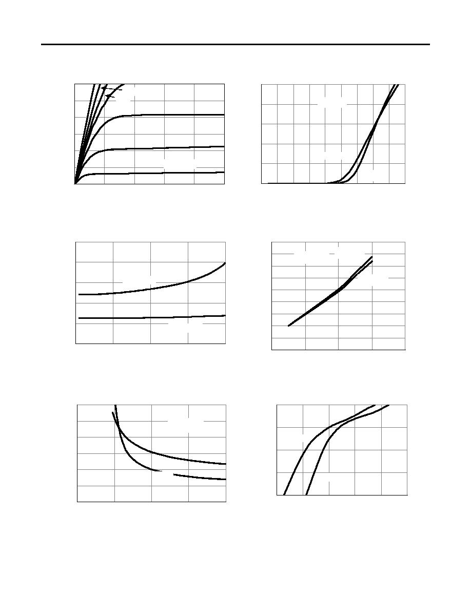
TYPICAL ELECTRICAL AND THERMAL CHARACTERISTICS: N-CHANNEL
0
5
10
15
20
25
30
0
1
2
3
4
5
V
DS
(Volts)
Fig 1: On-Region Characteristics
I
D
(A)
V
GS
=3V
3.5V
4V
4.5V
10V
0
4
8
12
16
20
0
0.5
1
1.5
2
2.5
3
3.5
4
4.5
V
GS
(Volts)
Figure 2: Transfer Characteristics
I
D
(A)
10
20
30
40
50
60
0
5
10
15
20
I
D
(Amps)
Figure 3: On-Resistance vs. Drain Current and Gate
Voltage
R
DS
(
O
N)
(m
)
1.0E-03
1.0E-02
1.0E-01
1.0E+00
1.0E+01
0.0
0.2
0.4
0.6
0.8
1.0
V
SD
(Volts)
Figure 6: Body diode characteristics
MOSFET+Schottky
I
S
Am
p
s
125∞C
0.8
0.9
1
1.1
1.2
1.3
1.4
1.5
1.6
1.7
0
50
100
150
200
Temperature ( ∞C)
Figure 4: On-Resistance vs. Junction Temperature
N
o
r
mal
i
z
ed
O
n
-
R
esi
st
an
ce
V
GS
=10V
V
GS
=4.5V
10
20
30
40
50
60
70
2
4
6
8
10
V
GS
(Volts)
Figure 5: On-Resistance vs. Gate-Source Voltage
R
DS
(
O
N)
(m
)
25∞C
125∞C
V
DS
=5V
V
GS
=4.5V
V
GS
=10V
I
D
=7.5A
125∞C
25∞C
25∞C
I
D
=7.5A
5V
6V
Alpha & Omega Semiconductor, Ltd.