
Fea tures
Ј
Narrow receiving angle
Ј
Variety of sensitivity ranges
Ј
T-1 package style
Ј
Small package size for space limited
applications
Ј
Base-emitter resistor provides ambient
light protection
De scrip tion
The OP705 series devices consist of
NPN silicon phototransistors molded in
blue tinted epoxy packages. The narrow
receiving angle provides excellent on-
axis coupling. These devices are 100%
production tested using infrared light for
close correlation with Optek
'
s GaAs and
GaAlAs emitters.
The phototransistor has an internal base-
emitter resistor which provides protection
from low level ambient lighting
conditions. This feature is also useful
when the media being detected is semi-
transparent to infrared light in interruptive
applications.
Ab so lute Maxi mum Rat ings (T
A
= 25
o
C un less oth er wise noted)
Collector- Emitter Volt age. . . . . . . . . . . . . . . . . . . . . . . . . . . . . . . . . . . . . . . . . . . . 30 V
Emit ter Re verse Current. . . . . . . . . . . . . . . . . . . . . . . . . . . . . . . . . . . . . . . . . . . 10 mA
Col lec tor DC Cur rent . . . . . . . . . . . . . . . . . . . . . . . . . . . . . . . . . . . . . . . . . . . . . 30 mA
Stor age and Op er at ing Tem pera ture Range. . . . . . . . . . . . . . . . . . -40
o
C to +100
o
C
Lead Sol der ing Tem pera ture [1/16 inch (1.6 mm) from case for 5 sec. with sol der ing
iron] . . . . . . . . . . . . . . . . . . . . . . . . . . . . . . . . . . . . . . . . . . . . . . . . . . . . . . . . 260
o
C
(1)
Power Dis si pa tion . . . . . . . . . . . . . . . . . . . . . . . . . . . . . . . . . . . . . . . . . . . . 100 mW
(2)
“±ђї-ж
(1) RMA flux is recommended. Duration can be extended to 10 sec. max. when flow soldering.
Max. 20 grams force may be applied to leads when soldering.
(2) Derate linearly 1.33 mW /
o
C above 25
o
C.
(3) Light source is an unfiltered GaAs LED with a peak emission wavelength of 935 nm and a
radiometric intensity level which varies less than 10% over the entire lens surface of the
phototransistor being tested.
(4) The knee point irradiance is defined as the irradiance required to increase I
C(ON)
to 50
ЈЈ
A.
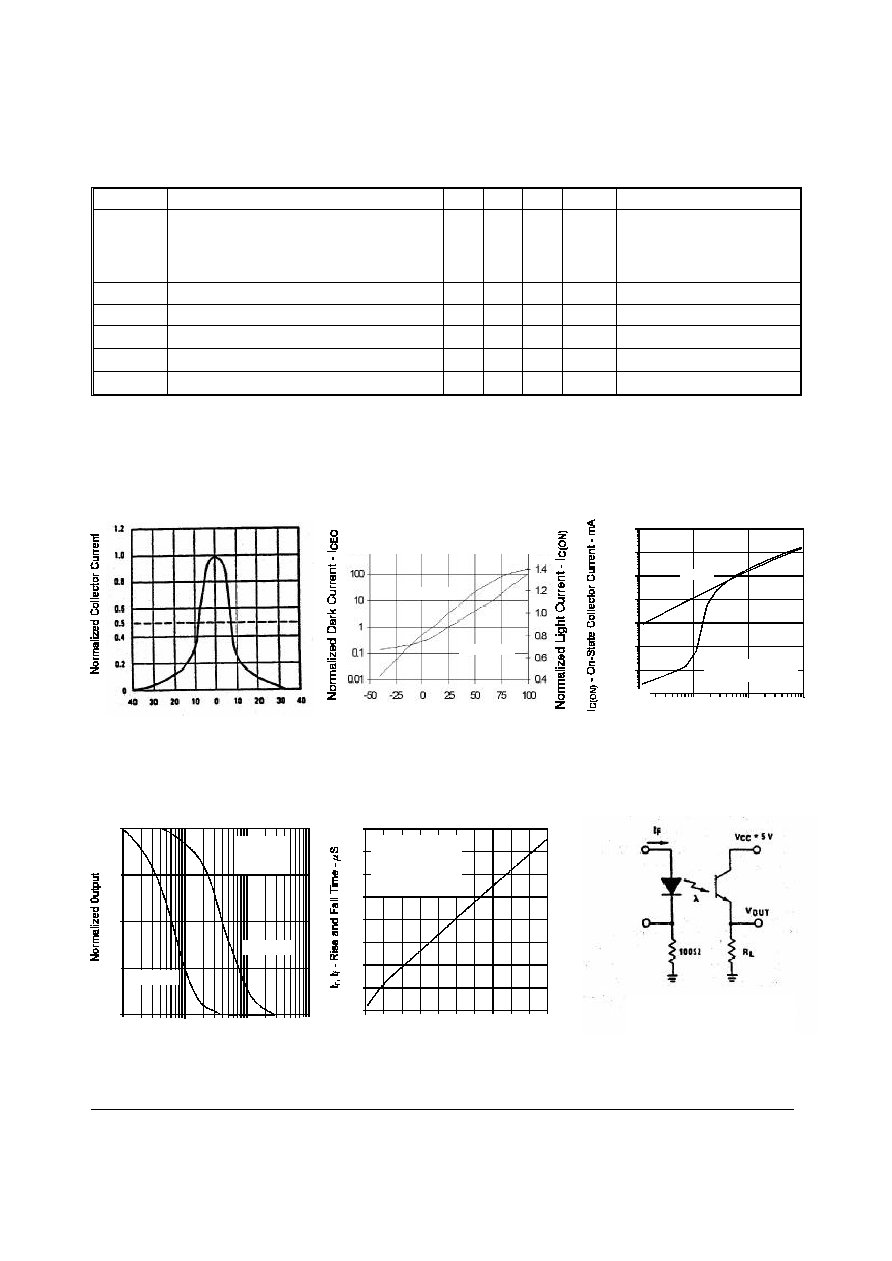
Typi cal Per form ance Curves
Prod uct Bul le tin OP705
March 1999
NPN Pho to tran sis
tor with Base-Emit ter Resistor
Types OP705A, OP705B, OP705C, OP705D
Op tek Tech nol ogy, Inc. 1215 W. Crosby Road Car roll ton, Texas 75006 (972) 323- 2200 Fax (972) 323- 2396
ћІ∞Ј љњі Ќ∞їљ ђЃњі ќї -∞±≤-ї
…њ™ї ії≤єђЄ у ≤≥
5
Sche matic
Types OP705A, OP705B, OP705C, OP705D
Optek reserves the right to make changes at any time in order to improve design and to supply the best product possible.
Op tek Tech nol ogy, Inc. 1215 W. Crosby Road Car roll ton, Texas 75006 (972) 323- 2200 Fax (972) 323- 2396
Elec tri cal Char ac ter is tics (T
A
= 25
o
C un less oth er wise noted)
SYM BOL
PA RAME TER
MIN TYP MAX UNITS
TEST CON DI TIONS
I
C(ON)
On-State Collector Current
OP705A
OP705B
OP705C
OP705D
3.95
2.65
1.50
1.50
12.0
7.25
4.85
12.0
mA
V
CE
= 5 V, E
e
= .50 mW/cm
2(3)
E
KP
Knee Point Irradiance
.02
mW/cm
2
V
CE
= 5 V
(4)
I
CEO
Collector-Emitter Dark Current
100
nA
V
CE
= 10 V, E
e
= 0
I
ECO
Emitter-Reverse Current
100
µ
A
V
EC
= 0.4 V
V
(BR)CEO
Collector-Emitter Breakdown Voltage
30
V
I
C
= 100
µ
A
V
CE(SAT)
Collector-Emitter Saturation Voltage
0.4
V
I
C
= 250
µ
A, E
e
= .50 mW/cm
2(3)
Typi cal Per form ance Curves
6
On-State Collector Current
vs. Irradiance
Normalized Collector Current
vs. Angular Displacement
Ј
- Angular Displacement - Deg.
—–лрл
Normalized Light and Dark
Current vs. Ambient Temperature
ћ
я
у я≥ЊЈї≤ђ ћї≥∞їЃњђЂЃї у ЈЈЁ
№њЃµ ЁЂЃЃї≤ђ
—–йрл
Normalized Output
vs. Frequency
Frequency - KHz
Typical Rise and Fall Time
vs. Load Resistance
ќ
‘
у ‘±њЉ ќї-Ј-ђњ≤љї у ’Ј
Switching Time
Test Circuit
ћї-ђ Ё±≤ЉЈђЈ±≤-ж
‘ЈєЄђ -±ЂЃљї Ј- ∞Ђі-їЉ ‘џ№ ©ЈђЄф ђЃ њ≤Љ
ђЇ Ј лрр ≤-т
„Џ Ј- њЉґЂ-ђїЉ Ї±Ѓ —Ћћ г п ±іђт
‘ЈєЄђ ЁЂЃЃї≤ђ
Ёџ г л
‘џ№ж Ј г знл ≤≥
птр
ртл
ртр
п
пр
прр
пррр
о
м
к
и
пр
нр
пл
р
мл
пор
прл
зр
йл
кр
прр
пр
п
тп
трп
тррп
трррп
тп
трп
п
E
e
- Irradiance - mW/cm2
тррррп
тррп
ќ‘ г п’Ј
ќ‘ г пр’Ј
V
CC
= 5 V
V
RL
= 1 V
f = 100 Hz
PW = 1 mS
LED = GaAIAS,
Ј
= 890 nm
V
RL
is voltage across R
L
р
V
RL
= 1 V
V
CE
= 5 V
50% Duty Cycle
LED:
Ј
= 935 nm