Fea tures
∑
0.125" (3.18 mm) wide gap
∑
Choice of mounting configuration
De scrip tion
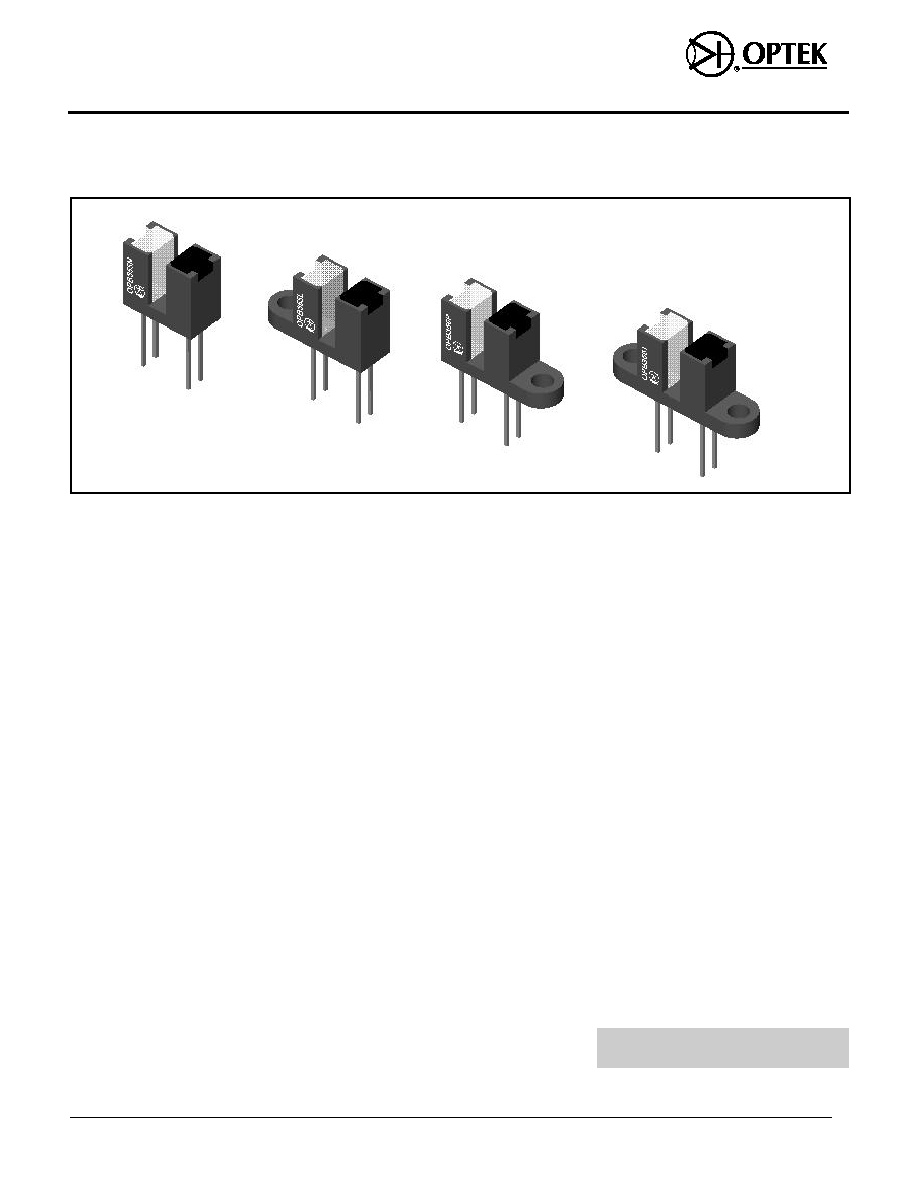
The OPB355 series of slotted switches
provides the design engineer with the
flexibility of a custom device from a
standard product line. Building from a
standard housing with a .125" (3.18 mm)
wide slot, the user can specify the
mounting tab configuration.
The photodiode output provides a lower
but more linear output vs. light input
when compared to slotted switches with
a standard phototransistor output.
All housings are an opaque grade of
injection molded plastic to minimize the
assembly's sensitivity to ambient
radiation, both visible and near-infrared.
Discrete shells (exposed on the parallel
faces inside the device throat) are IR
transmissive plastic for applications
where aperture contamination is a
concern.
Custom electrical, wire and cabling is
available. Contact your local
representative or Optek for more
information.
Ab so lute Maxi mum Rat ings (T
A
= 25
o
C un less oth er wise noted)
Stor age and Op er ating Tem per a ture Range . . . . . . . . . . . . . . . . . . . . -40
∞
C to +85
∞
C
Lead Sol dering Tem per a ture Range [1/16 inch (1.6 mm) from case for 5 sec. with sol -
der ing iron] . . . . . . . . . . . . . . . . . . . . . . . . . . . . . . . . . . . . . . . . . . . . . . . . . . . 240
∞
C
(2)
Input Di ode
For ward DC Cur rent . . . . . . . . . . . . . . . . . . . . . . . . . . . . . . . . . . . . . . . . . . . . . . 50 mA
Peak For ward Cur rent (1
µ
s pulse width, 300 pps) . . . . . . . . . . . . . . . . . . . . . . . . 3.0 A
Re verse DC Volt age . . . . . . . . . . . . . . . . . . . . . . . . . . . . . . . . . . . . . . . . . . . . . . . 2.0 V
Power Dis si pa tion . . . . . . . . . . . . . . . . . . . . . . . . . . . . . . . . . . . . . . . . . . . . . 100 mW
(1)
Out put Di ode
Re verse Break down Volt age . . . . . . . . . . . . . . . . . . . . . . . . . . . . . . . . . . . . . . . . . 60 V
Power Dis si pa tion . . . . . . . . . . . . . . . . . . . . . . . . . . . . . . . . . . . . . . . . . . . . . 100 mW
(1)
NOTES:
(1) De rate lin early 1.67 mW/
∞
C above 25
∞
C.
(2) RMA flux is rec om mended. Du ra tion can be ex tended to 10 sec. max. when flow sol der ing.
(3) All pa ram e ters tested us ing pulse tech nique.
(4) Po lar ity is de noted by color of hous ing top:
LED - Clear
Sen sor - Black
PRECAUTIONS: Ex po sure of the plas tic body to chlo ri nated hy dro car bons and ke tones such as
thread lock and in stant ad he sive prod ucts will de grade the plas tic body. Cleaning agents
meth a nol and isopropanol are rec om mended. Spray or wipe do not sub merge.
Prod uct Bul le tin OPB355
No vem ber 2000
Slotted Op ti cal Switches
Type OPB355 Se ries (Photodiode Out put)
Op tek Tech nol ogy, Inc. 1215 W. Crosby Road Car roll ton, Texas 75006 (972) 323- 2200 Fax (972) 323- 2396
Visit our website at www.optekinc.com
or email us at sensors@optekinc.com

Types OPB355 Series
Op tek re serves the right to make changes at any time in or der to im prove de sign and to sup ply the best prod uct pos si ble
Op tek Tech nol ogy, Inc. 1215 W. Crosby Road Car roll ton, Texas 75006 (972)323- 2200 Fax (972)323- 2396
Elec tri cal Char ac ter is tics (T
A
= 25
o
C un less oth er wise noted)
SYM BOL
PA RAM E TER
MIN TYP MAX UNITS
TEST CON DI TIONS
In put Di ode
V
F
Forward Voltage
1.30
1.8
V
I
F
= 20 mA
I
R
Reverse Current
100
µ
A
V
R
= 2 V
Out put Diode
V
BR
Reverse Diode Breakdown Voltage
60
V
I
R
= 100
µ
A, I
F
= 0, E
e
= 0
V
FD
Forward Voltage Photodiode
1.2
V
I
F
= 1 mA, I
F
= 0, E
e
= 0
I
D
Reverse Dark Current
60
nA
V
R
= 30 V, IF = 0, E
e
= 0
Cou pled
I
L
On-State Collector Current
OPB355T, N, L, P
10
200
µ
A
V
R
= 5 V, I
F
= 40 mA
PART NUMBER GUIDE
OPB 3 5 5 X
Optek
Assembly
Photodiode
Output Family
Mounting Configurations
T - Both Mounting Tabs
N - No Mounting Tabs
L - Single Mounting Tabs
Emitter Side
P - Single Mounting Tab
Photodiode Side
