
Fea tures
∑
Focused for maximum sensitivity
∑
Phototransistor (OPB702) or
Photodarlington (OPB702D) or
Phototransistor with
base-emitter
resistor (OPB702R)
∑
Low cost plastic housing
De scrip tion
The OPB702 family consists of an
infrared emitting diode and a choice of
NPN silicon phototransistor (OPB702),
photodarlington (OPB702D), or
base-emitter resistor for low light
suppresion (OPB702R). The IR LED
and phototransistor are mounted
side-by-side on converging optical axes,
in a black plastic housing.
Both parts are constructed using either
OP165 or OP265 series LEDs. The
OPB702 uses and OP505 type. The
OPB702D uses an OP535 type. The
OPB702R uses an OP705.
Custom electrical, wire or cabling is
available. Contact your local
representative or Optek for more
information.
Ab so lute Maxi mum Rat ings (T
A
= 25
o
C un less oth er wise noted)
Stor age and Op er ating Tem per a ture Range . . . . . . . . . . . . . . . . . . . . -40
∞
C to +85
∞
C
Lead sol der ing tem per a ture (1/16 inch [1.6 mm] from case for 5 sec. with sol der ing
iron) . . . . . . . . . . . . . . . . . . . . . . . . . . . . . . . . . . . . . . . . . . . . . . . . . . . . . . . . . 240
∞
C
(2)
In put Di ode
Re verse Volt age . . . . . . . . . . . . . . . . . . . . . . . . . . . . . . . . . . . . . . . . . . . . . . . . . . 2.0 V
Peak For ward Cur rent . . . . . . . . . . . . . . . . . . . . . . . . . . . . . . . . . . . . . . . . . . . . . 50 mA
Power Dis si pa tion . . . . . . . . . . . . . . . . . . . . . . . . . . . . . . . . . . . . . . . . . . . . . 100 mW
(1)
Out put Photosensor
Col lec tor-Emitter Volt age - OPB702 & OPB702R . . . . . . . . . . . . . . . . . . . . . . . . . 30 V
OPB702D . . . . . . . . . . . . . . . . . . . . . . . . . . . . . . . . . . 15 V
Emit ter-Collector Volt age - OPB702 & OPB702D . . . . . . . . . . . . . . . . . . . . . . . . . 5.0 V
Power Dis si pa tion - OPB702 & OPB702D & OPB702R . . . . . . . . . . . . . . . . 100 mW
(1)
NOTES:
(1) Derate linearly 1.67 mW/
∞
C above 25
∞
C.
(2) RMA flux is recommended. Duration can be extended to 10 sec. max. when flow soldering.
(3) d is the distance from the assembly face to the reflective surface.
(4) Measured using Eastman Kodak gray card. The white side of the card is used as a 90%
diffuse reflectance surface. Reference Eastman Kodak, Catalog #E152 7795.
(5) All parameters tested using pulse techniques.
(6) Lead spacing controlled at body egress.
PRECAUTIONS: Exposure of the plastic body to chlorinated hydrocarbons and ketones such
as thread lock and instant adhesive products will degrade the plastic body. Cleaning agents
methanol and isopropanol are recommended. Spray or wipe do not submerge.
Prod uct Bul le tin OPB702
Oc to ber 2000
Re flec tive Ob ject Sensors
Type OPB702, OPB702D, OPB702R
Op tek Tech nol ogy, Inc. 1215 W. Crosby Road Car roll ton, Texas 75006 (972) 323- 2200 Fax (972) 323- 2396
Visit our website at www.optekinc.com
or email us at sensors@optekinc.com
Type OPB702
Op tek re serves the right to make changes at any time in or der to im prove de sign and to sup ply the best prod uct pos si ble
Op tek Tech nol ogy, Inc. 1215 W. Crosby Road Car roll ton, Texas 75006 (972)323- 2200 Fax (972)323- 2396
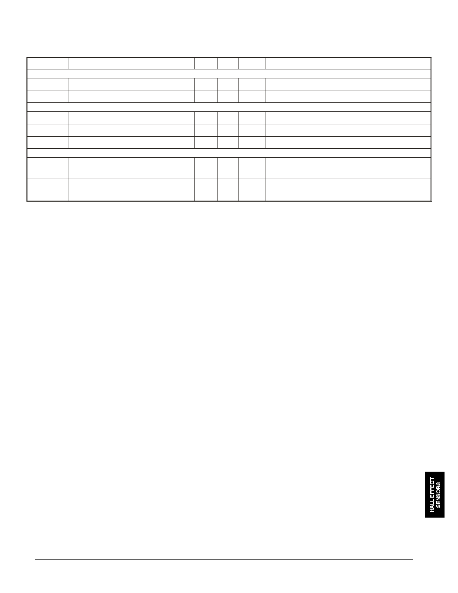
Electrical Characteristics (T
A
= 25
∞
C unless otherwise noted)
SYM BOL
PA RAME TER
MIN MAX UNITS
TEST CON DI TIONS
In put Di ode
V
F
Forward Voltage
1.8
V
I
F
= 20 mA
I
R
Reverse Current
100
µ
A
V
R
= 2.0 V
Out put Phototransistor
V
(BR)CEO
Collector-Emitter Breakdown Voltage
30
V
I
C
= 100
µ
A, I
F
= 0, E
e
= 0
V
(BR)ECO
Emitter-Collector Breakdown Voltage
5.0
V
I
E
= 100
µ
A, I
F
= 0, E
e
= 0
I
CEO
Collector-Emitter Leakage Current
100
nA
V
CE
= 10 V, I
F
= 0, E
e
= 0
Cou pled
I
C(ON)
On-State Collector Current
50
µ
A
V
CE
= 5.0 V, I
F
= 40 mA,
d = 0.150" (3.81 mm)
(3)(4)
V
CE(SAT)
Collector-Emitter Saturation Voltage
0.40
V
I
C
= 250
µ
A, I
F
= 40 mA,
d = 0.150" (3.81 mm)
(3)(4)
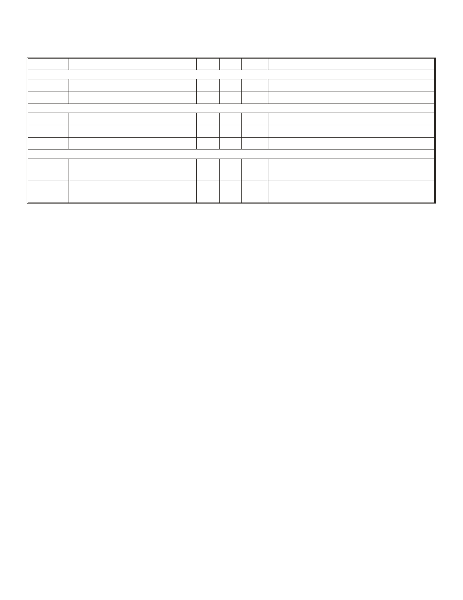
Type OPB702D
Electrical Characteristics (T
A
= 25
∞
C unless otherwise noted)
SYM BOL
PA RAME TER
MIN MAX UNITS
TEST CON DI TIONS
In put Di ode
V
F
Forward Voltage
1.8
V
I
F
= 20 mA
I
R
Reverse Current
100
µ
A
V
R
= 2.0 V
Out put Phototransistor
V
(BR)CEO
Collector-Emitter Breakdown Voltage
15.0
V
I
C
= 1 mA, I
F
= 0 , E
e
= 0
V
(BR)ECO
Emitter-Collector Breakdown Voltage
5.0
V
I
E
= 100
µ
A, I
F
= 0, E
e
= 0
I
CEO
Collector-Emitter Leakage Current
250
nA
V
CE
= 10.0 V, I
F
= 0, E
e
= 0
Cou pled
I
C(ON)
On-State Collector Current
2.0
mA
V
CE
= 5.0 V, I
F
= 40 mA,
d = 0.150" (3.81 mm)
(3)(4)
V
CE(SAT)
Collector-Emitter Saturation Voltage
1.10
V
I
C
= 400
µ
A, I
F
= 40 mA,
d = 0.150" (3.81 mm)
(3)(4)

Type OPB702R
Elec tri cal Char ac ter is tics (T
A
= 25
o
C un less oth er wise noted)
SYM BOL
PA RAME TER
MIN MAX UNITS
TEST CON DI TIONS
In put Di ode
V
F
Forward Voltage
1.8
V
I
F
= 20 mA
I
R
Reverse Current
100
µ
A
V
R
= 2.0 V
Out put Phototransistor
V
(BR)CEO
Collector-Emitter Breakdown Voltage
30
V
I
C
= 100
µ
A, I
F
= 0, E
e
= 0
I
ECO
Emitter-Reverse Current
100
µ
A
V
EC
= 0.4 V, I
F
= 0, E
e
= 0
I
CEO
Collector-Emitter Leakage Current
100
nA
V
CE
= 10.0 V, I
F
= 0, E
e
= 0
Cou pled
I
C(ON)
On-State Collector Current
50
µ
A
V
CE
= 5.0 V, I
F
= 40 mA,
d = 0.150" (3.81 mm)
(3)(4)
V
CE(SAT)
Collector-Emitter Saturation Voltage
0.40
V
I
C
= 250
µ
A, I
F
= 40 mA,
d = 0.150" (3.81 mm)
(3)(4)