 | –≠–ª–µ–∫—Ç—Ä–æ–Ω–Ω—ã–π –∫–æ–º–ø–æ–Ω–µ–Ω—Ç: OPF5112 | –°–∫–∞—á–∞—Ç—å:  PDF PDF  ZIP ZIP |

Optek Technology, Inc.
1215 West Crosby Road
Carrollton, Texas 75006
(972) 323-2200
www.optekinc.com
Technical Data
OPF5112
Features
∑
1310nm LED
∑
Data Rate: 155Mbps, NRZ
∑
Single +3.3V Power Supply
∑
PECL Differential Electrical Interface
∑
Industry Standard 1X 9 Form Factor
∑
Duplex ST Connector
∑
Compliance with:
∑
100Base -FX of IEEE802.3u Standard
∑
FDDI PMD Standard
∑
Eye Safety:
∑
Designed to meet Laser Class 1
Compliance with EN60825-1
Transmitter
The transmitter section is a 1300nm LED and a driver
circuit which converts the differential, PECL digital input
signals into an proportional LED drive current. Because
the 1300nm wavelength takes advantage of the lower
dispersion and attenuation region of glass optical fiber,
this transceiver is capable of link distances of 2km at the
maximum data rate.
Receiver
The receiver optical sub-assembly consists of a InGaAs
PIN photodiode and transimpedance amplifier in an inte-
grated package to optimize performance. The resulting
analog output is coupled to a post-amplifier for signal con-
ditioning and conversion to differential, PECL high-speed
outputs.
Description
The OPF5112 from Optek is a high performance,
cost effective module for serial optical data commu-
nications applications specified for 100 Mb/s opera-
tion. This transceiver operates with +3.3V power
supply and is housed in a plastic package with an
industry standard 1 x 9 form factor.
The OPF5112 is a duplex ST transceiver designed
for use in Fast Ethernet 100 Base-FX interface. The
characterization is performed in accordance FDDI
PMD Standard. Likewise, the Fast Ethernet Alliance
defines the Physical Layer for 100 Base-FX for Fast
Ethernet to be the FDDI PMD Standard.
OPF5112 consists of a transmitter optical subas-
sembly, a receiver optical subassembly and an
electrical sub-assembly. All are housed in a plastic
package and the combination produces a compo-
nent of high performance and reliability.
Applications
∑
Fast Ethernet
∑
FDDI
∑
ATM
∑
SONET
∑
Multimode fiber links
∑
Optical-Electrical Interface Conversion
1300nm Fast Ethernet
Transceiver in 1 x 9 ST
Duplex Package

Optek Technology, Inc.
1215 West Crosby Road
Carrollton, Texas 75006
(972) 323-2200
www.optekinc.com
OPF5112 Technical Data
Regulatory Compliance
The OPF5112, and other products from Optek, are
designed to comply with regulations governing
equipment used in information technology equip-
ment. The goal is for seamless integration of these
products into system designs with the confidence
that the requirements set forth by the certifying
body will be met. For more information, please con-
tact an Optek sales representative or applications
engineer.
Electromagnetic Interference (EMI)
EMI compliance is governed by different organiza-
tions throughout the world:
∑
The FCC in the United States
∑
CENELEC EN55022 in Europe
∑
VCCI in Japan
The OPF5112 has been design to comply with FCC
standards and meet the Class B limits specified
therein.
Immunity
Some locations that data communications equip-
ment is located have high levels of radio-frequency
electromagnetic fields. The OPF5112 exhibits ex-
cellent immunity to these fields.
Eye Safety
All Optek transceivers emit invisible radiation from
their optical connector ports. As such, precautions
should be taken when using these devices. Optek
transceiver products are designed to meet Class 1
eye safety guidelines and comply with EN60825-1.
Electrostatic Discharge
The OPF5112 is subject to damage from ESD.
Normal ESD handling practices should be observed
when handling this device. Grounded wrist straps,
work stations and floor mats are advised.
DATA IN
DATA IN
Block Diagram
DATA OUT
DATA OUT
SIGNAL DETECT
Transmitter Sub-Assembly
Receiver Sub-Assembly
LED Driver IC
Post-Amplifier/ Quantizer IC
Optek Technology, Inc.
1215 West Crosby Road
Carrollton, Texas 75006
(972) 323-2200
www.optekinc.com
OPF5112 Technical Data
N/C
N/C
1=V
EER
2=RD+
3=RD-
4=SD
5=V
CCR
6=V
CCT
7=TD-
8=TD+
9=V
EET
Pin
Symbol
Functional Description
Mounting Posts
The mounting posts are provided for transceiver mechanical attachment to the circuit board. They
should not be connected to the circuit ground but can be connected to the chassis ground.
1
V
EER
Receiver Signal Ground
2
RD+
Receiver Data Non-inverted Differential Output
3
RD-
Receiver Data Inverted Differential Output
4
SD
Signal Detect is a PECL output. A high level indicates a received optical signal
5
V
CCR
+3.3 V Receiver Power Supply
6
V
CCT
+3.3 V Transmitter Power Supply
7
TD-
Transmitter Data Inverted Differential Input
8
TD+
Transmitter Data Non-inverted Differential Input
9
V
EET
Transmitter Signal Ground
Transceiver Pin Out Diagram
Transceiver Pin Out Table

Optek Technology, Inc.
1215 West Crosby Road
Carrollton, Texas 75006
(972) 323-2200
www.optekinc.com
OPF5112 Technical Data
Parameter
Symbol
Min
Typ
Max
Units
Test Conditions
Ambient Operating Temperature
T
A
0
70
∞
C
Supply Voltage
V
CC
3.135
3.465
V
High Level Input Voltage
V
IH ≠
V
CC
-1.165
-0.880
V
Low Level Input Voltage
V
IL
-
V
CC
-1.810
-1.620
V
Absolute Maximum Ratings
Recommended Operating Conditions
Parameter
Symbol
Min
Typ
Max
Units
Test Conditions
Storage Temperature
T
S
-40
85
∞
C
Soldering Temperature
T
SOLD
260
V
10 Seconds
Supply Voltage
V
CC
-0.5
3.6
V
Input Voltage
V
I
-0.5
V
CC
V
Parameter
Symbol
Min
Typ
Max
Units
Test Conditions
Supply Current
I
CC
165
mA
Power Dissipation
P
D
870
mW
Data Input Current--High
I
IH
-350
µA
Note 1
Data Input Current--Low
I
IL
350
µA
Note 1
Transmitter Electrical Characteristics
(T
A
= 0 to 70 ∞C, V
CC
= 3.135 to 3.465V)
Receiver Electrical Characteristics
(T
A
= 0 to 70 ∞C, V
CC
= 3.135 to 3.465V)
Parameter
Symbol
Min
Typ
Max
Units
Test Conditions
Supply Current
I
CC
95
mA
Power Dissipation
P
D
500
mW
Receiver Data Output Voltage ≠ Low
V
OL
-V
CC
-1.810
-1.620
V
Note 2
Receiver Data Output Voltage ≠ High
V
OH
-V
CC
-1.025
-0.880
V
Note 2
Signal Detect Output Voltage - Low
V
OL
-V
CC
-1.810
-1.620
V
Note 2
Signal Detect Output Voltage - High
V
OH
-V
CC
-1.025
-0.880
V
Note 2

Optek Technology, Inc.
1215 West Crosby Road
Carrollton, Texas 75006
(972) 323-2200
www.optekinc.com
OPF5112 Technical Data
Parameter
Symbol
Min
Typ
Max
Units
Test Conditions
Coupled Optical Power
P
O
-19
-14
dBm
Note 3
Optical Extinction Ratio
ER
10
dB
Note 4,5
Center Wavelength
?
C
1270
1360
nm
Spectral Width (FWHM)
??
170
nm
Optical Rise Time
t
r
0.6
3.0
ns
Note 4
Optical Fall Time
t
f
0.6
3.0
ns
Note 4
Total Jitter
t
RJ
0.69
ns
Note 6
Duty Cycle Distortion≠ Transmitter
Transmitter Electrical Characteristics
(T
A
= 0 to 70 ∞C, V
CC
= 3.135 to 3.465V)
Parameter
Symbol
Min
Typ
Max
Units
Test Conditions
Maximum Input Optical Power
P
MAX
-14
-11
dBm
Note 6
Receiver Sensitivity
P
MIN
-34
-32
dBm
Note 6
Operating Wavelength
?
1100
1600
nm
Signal Detect--Asserted
P
A
-33
dBm
Signal Detect--Deasserted
P
D
-45
dBm
Note 7
Signal Detect--Hysteresis
P
A
-P
D
1.5
dB
Note 8
Random Jitter--Receiver Contribution
RJ
2.14
ns
Receiver Electrical Characteristics
(T
A
= 0 to 70 ∞C, V
CC
= 3.135 to 3.465V)
Notes:
1. Compatible with 10K , 10KH , 100K ECL and PECL output signals.
2. These outputs are compatible with 10K , 10KH , 100K ECL and PECL inputs.
3. Measured average power coupled into 62.5/125µm, 0.275 NA graded index multimode fiber
4. The input data pattern is a 12.5MHz square wave pattern.
5. Extinction Ratio = 10*LOG
10
(PH / PL)
6. Measured with 2
23
-1 PRBS at BER<1x10
-10
7. Measured on transition ≠ low to high
8. Measured on transition ≠ high to low

Optek Technology, Inc.
1215 West Crosby Road
Carrollton, Texas 75006
(972) 323-2200
www.optekinc.com
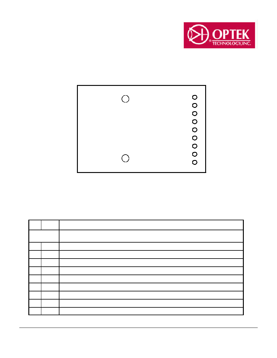
Mechanical Dimensions
OPF5112 Technical Data
Optek reserves the right to make changes at any time in order to improve design and to supply the best product possible.
November 2002
OPF5112, Rev. B