Fea tures
∑
Four out put op tions
∑
High noise im mu nity
∑
Di rect TTL/LSTTL CMOS in ter face
∑
Low cost plas tic side- looking pack age
∑
Me chani cally and spec trally matched
to the OP140 and OP240 se ries LED's
∑
Data rates to 250 kBaud
∑
Low power con sump tion
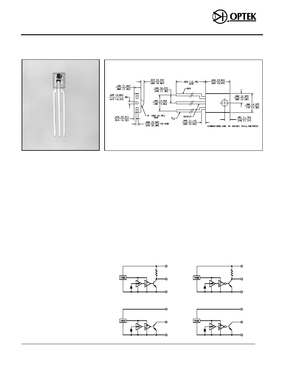
De scrip tion
The OPL530, OPL530-OC, OPL531,
OPL531-OC contain a monolithic
integrated circuit which incorporates a
photodiode, amplifier, voltage regulator,
Schmitt trigger and an NPN output
transistor on a single silicon chip.
The OPL530 and OPL531 includes a 10
K
pull-up resistor (R
L
) from output to
V
CC
. The OPL530-OC and OPL531-OC
have an open-collector output.
These devices exhibit very stable
performance over supply voltages
ranging from 4.5 V to 16 V and a wide
range of irradiance levels.
The Photologic
Æ
chip is encapsulated in
a molded plastic package which has an
integral lens for enhanced optical
coupling and minimal optical spacing.
Ab so lute Maxi mum Rat ings (T
A
= 25
o
C un less oth er wise noted)
Sup ply Volt age, V
CC
. . . . . . . . . . . . . . . . . . . . . . . . . . . . . . . . . . . . . . . . . . . . . . . 18 V
Stor age Tem pera ture Range . . . . . . . . . . . . . . . . . . . . . . . . . . . . . . -40
o
C to +100
o
C
Op er at ing Tem pera ture Range . . . . . . . . . . . . . . . . . . . . . . . . . . . . . -40
o
C to +85
o
C
Lead Sol der ing Tem pera ture Range [1/16 inch (1.6 mm) from case for 5 sec. with
sol der ing iron] . . . . . . . . . . . . . . . . . . . . . . . . . . . . . . . . . . . . . . . . . . . . . . . . . . 240
o
C
Power Dis si pa tion . . . . . . . . . . . . . . . . . . . . . . . . . . . . . . . . . . . . . . . . . . . . . . . 90 mW
Volt age at Out put Lead
(4)
. . . . . . . . . . . . . . . . . . . . . . . . . . . . . . . . . . . . . . . . . . . 35 V
Sink ing Cur rent . . . . . . . . . . . . . . . . . . . . . . . . . . . . . . . . . . . . . . . . . . . . . . . . . . 50 mA
Notes:
(1) Derate linearly 2.67 mW/
o
C above 70
o
C.
(2) RMA flux is recommended. Duration can be extended to 10 sec. maximum when flow
soldering. Max 20 grams force may be applied to the leads when soldering.
(3) Irradiance measurements are made with
i = 935 nm.
(4) OC versions only. For I
CC
on pull-up versions add V
CC
/10 k
.
Sche mat ics
Prod uct Bul le tin OPL530
December 1997
Pho tologic
Æ
Sen sors
Types OPL530, OPL530- OC, OPL531, OPL531- OC
Op tek Tech nol ogy, Inc. 1215 W. Crosby Road Car roll ton, Texas 75006 (972) 323- 2200 Fax (972) 323- 2396
OPL530 Buffer/Pull- up Re sis tor
OPL531 Inverter/Pull- up Re sis tor
OPL530- OC Buffer/OC
OPL531- OC Inverter/OC
Light On - Out put High
Light On - Out put Low
Light On - Out put High
Light On - Out put Low
V
CC
OUT
GND
V
CC
OUT
GND
V
CC
OUT
GND
V
CC
OUT
GND
4-4
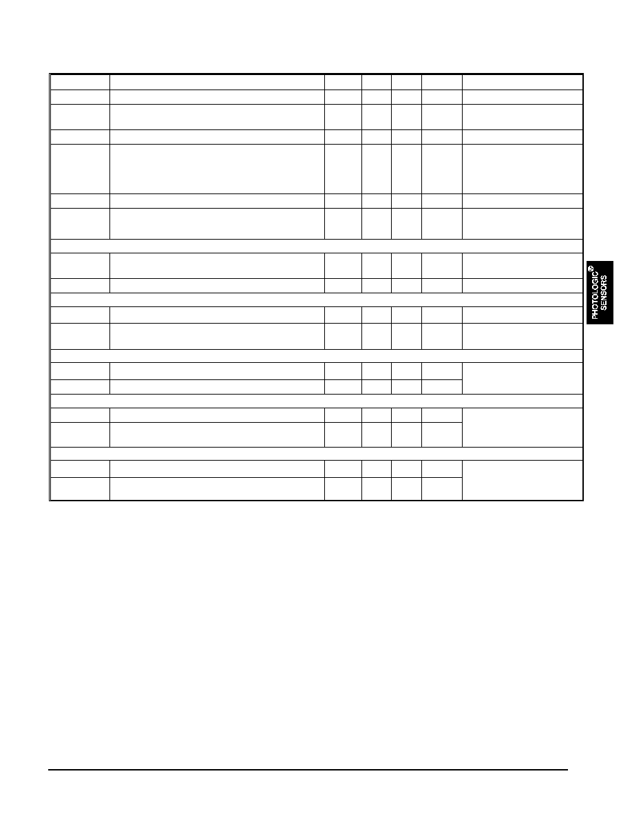
Types OPL530, OPL530-OC, OPL531, OPL531-OC
Elec tri cal Char ac ter is tics (-40
o
C to +85
o
C un less oth er wise noted) V
CC
= 4.5 V to 16 V
SYM BOL
PA RAME TER
MIN
TYP MAX UNITS
TEST CON DI TIONS
V
CC
Operating Supply Voltage
4.5
16.0
V
Peak-to-Peak V
CC
Ripple Necessary to Cause
False Triggering of Output
2
V
f = DC to 50 MHz
I
CC
Supply Current
(4)
2.7
5.0
mA
E
e
= 0 or 1 mW/cm
2
E
eT
(+)
Positive-Going Threshold Irradiance
(3)
OPL530, OPL530-OC, OPL531, OPL531-OC
OPL530A, OPL530-OCA, OPL531A, OPL531-OCA
OPL530B, OPL530-OCB,OPL531B, OPL531-OCB
0.12
0.12
0.23
0.38
0.28
0.38
mW/cm
2
mW/cm
2
mW/cm
2
T
A
= 25
o
C
T
A
= 25
o
C
T
A
= 25
o
C
E
eT
(+)/E
eT
(-) Hysteresis Ratio
1.20
1.80
E
eT
(+)(
T)
Temperature Coefficient
>
0
o
C
<
0
o
C
-0.6
-1.6
%/
o
C
%/
o
C
OPL530, OPL530- OC (Buff ers)
I
OH
High Level Output Current
(4)
0.1
10
µ
A
V
OH
= 30 V,
E
e
= 1 mW/cm
2
V
OL
Low Level Output Voltage
0.2
0.40
V
I
OL
= 16 mA, E
e
= 0
OPL531, OPL531- OC (Invert ers)
I
OH
High Level Output Current
(4)
0.1
10
µ
A
V
OH
= 30 V, E
e
= 0
V
OL
Low Level Output Voltage
0.2
0.40
V
I
OL
= 16 mA,
E
e
= 1 mW/cm
2
OPL530, OPL531
t
r
Output Rise Time
1.5
µ
s
E
e
= 0 or 1 mW/cm
2
,
C
L
= 50 pF
t
f
Output Fall Time
20
ns
OPL530- OC, OPL531- OC
t
r
Output Rise Time
50
ns
E
e
= 0 or 1 mW/cm
2
,
R
L
= 300
to 5 V,
C
L
= 50 pF
t
f
Output Fall Time
20
ns
OPL530, OPL530- OC, OPL531, OPL531- OC
tpE
eT
(+)
Propagation Delay
1.0
µ
s
E
e
= 0 or 1 mW/cm
2,
R
L
= 300
to 5 V,
C
L
= 50 pF
tpE
eT
(-)
Propagation Delay
3.0
µ
s
Optek Reserves the right to make changes at any time in order to improve design and to supply the best product possible.
Optek Technology, Inc. 1215 W. Crosby Road Carrollton, Texas 75006 (972)323-2200 Fax (972)323-2396
4-5