Fea tures
∑
Surface mountable
∑
Multiple channels available
∑
TTL compatible output
∑
Wide supply voltage range
De scrip tion
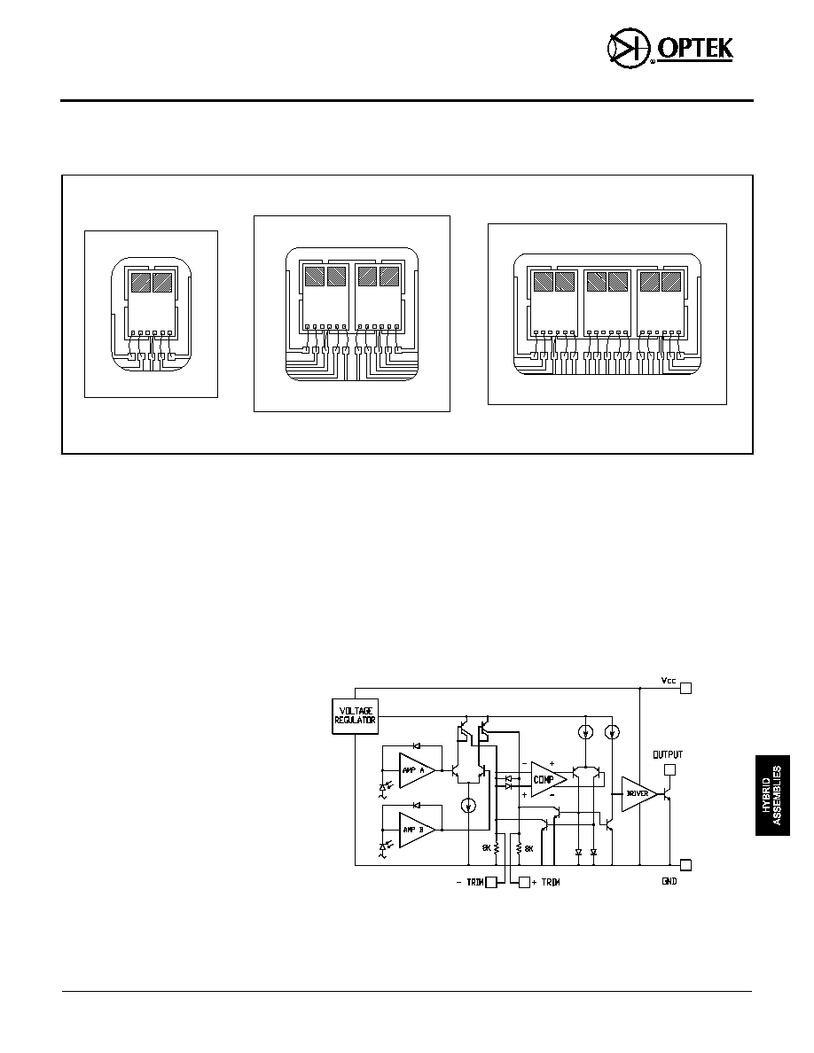
The OPR5001B, OPR5002B and
OPR5003B are hybrid sensor arrays
consisting of one, two or three channels
of the Optek OPC8032 Differential
Optical Comparator, ("DOC") IC.
Specifically designed for encoder
applications, the open collector output
switches based on the comparison of
input photodiode's light current levels.
Logarithmic amplification of the input
signals makes possible operation over a
wide range of light levels.
The packages are surface mountable
and made from a custom opaque
polyimide which shields the active
devices from stray light. The high
temperature laminate can withstand
multiple exposures to the most
demanding soldering conditions. Wrap
around contacts are gold plated for
exceptional storage and wetting
characteristics.
Replaces OPR5001A Series.
Ab so lute Maxi mum Rat ings (T
A
= 25
o
C un less oth er wise noted)
Stor age Tem pera ture . . . . . . . . . . . . . . . . . . . . . . . . . . . . . . . . . . . . -55
o
C to +125
o
C
Op er at ing tem pera ture . . . . . . . . . . . . . . . . . . . . . . . . . . . . . . . . . . . . -20
o
C to +80
o
C
Sup ply Volt age . . . . . . . . . . . . . . . . . . . . . . . . . . . . . . . . . . . . . . . . . . . . . . . . . . . 24 V
Out put Volt age. . . . . . . . . . . . . . . . . . . . . . . . . . . . . . . . . . . . . . . . . . . . . . . . . . . . 24 V
Out put Cur rent . . . . . . . . . . . . . . . . . . . . . . . . . . . . . . . . . . . . . . . . . . . . . . . . . . 14 mA
Power Dis si pa tion . . . . . . . . . . . . . . . . . . . . . . . . . . . . . . . . . . . . . . . . . . . . . . 500 mW
Sol der ing Tem pera ture (Va por Phase Re flow for 30 sec.) . . . . . . . . . . . . . . . . 235
o
C
Prod uct Bul le tin OPR5001B
Janu ary 1998
Optical Comparator Arrays
Type OPR5001B, OPR5002B, OPR5003B
Op tek Tech nol ogy, Inc. 1215 W. Crosby Road Car roll ton, Texas 75006 (972) 323- 2200 Fax (972) 323- 2396
OPC8032 Block Dia gram
9-19
Type OPR5001B, OPR5002B, OPR5003B
Elec tri cal Char ac ter is tics (T
A
= 25
o
C un less oth er wise noted)
SYM BOL
PA RAME TER
MIN TYP MAX UNITS
TEST CON DI TIONS
NOTES
I
CC
Supply Current
5001
3
7
mA
V
CC
= 24 V
1
5002
6
14
mA
5003
9
20
mA
V
OL
Low Level Output Voltage
0.3
0.4
V
I
OL
= 14 mA, V
CC
= 4.5 V
2
I
OH
High Level Output Current
0.1
1.0
µ
A
V
CC
= V
O
= 20.0 V
3
OPT-HYS Optical Hysteresis
2.0
15.0
40
%
V
CC
= 5.0 V, I
OL
= 1.0 mA
4, 7
OPT-OFF Optical Offset
-40
10
+40
%
V
CC
= 5.0 V, I
OL
= 1.0 mA
4, 7
fmax
Frequency Response
300
kHz
V
CC
= 5.0 V
5
tlh
Output Rise Time
2.0
µ
s
6
thl
Output Fall Time
500
ns
Notes:
1. Pin (+) = 1.2
µ
W and Pin (-) = 0.8
µ
W.
2. Pin (+) = 100.0 nW and Pin (-) = 1.0
µ
W.
3. Pin (+) = 1.0
µ
W and Pin (-) 100.0 nW.
4. Pin (-) held at 1.0
µ
W while Pin (+) is ramped from 0.5
µ
W to 1.5
µ
W and back to 0.5
µ
W.
5. Pin (+) modulated from 1.0
µ
W to 2.0
µ
W. Pin (-) modulated from 1.0
µ
W to 2.0
µ
W with phase shifted 180
o
with respect to Pin (+). Use 100
k
trimpot to set the output signal to 50% duty cycle for maximum operating frequency.
6. Measured between 10% and 90% points.
7. Optical Hysteresis and Optical Offset are found by placing 1.0
µ
W of light on the inverting photodiode and ramping the light intensity of the
noninverting input from .5
µ
W up to 1.5
µ
W and back down. This will produce two trigger points, an upper trigger point and lower trigger point.
These points are used to calculate the optical hysteresis and offset.
These are de fined as:
% Optical Hysteresis = 100 x (P rise - P fall)
P in (-)
% Optical Offset
= 100 x (P average - P (-) )
P in (-)
Where:
P in (-) = Light level incident upon the "-" photodiode on the I.C. chip (Pin (-) = 1.0
µ
W).
P rise = Value of light power level incident upon the "+" photodiode that is required to switch the digital output when the light level is an
increasing level (rising edge).
P fall = Value of light power level incident upon the "+" photodiode that is required to switch the digital output when the light level is a
decreasing level (falling edge).
P average = (P rise + P fall)
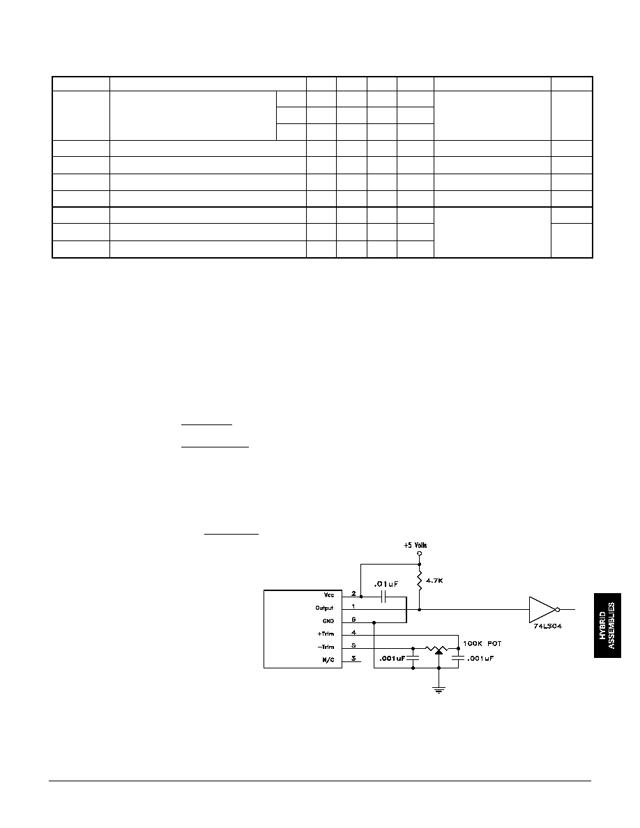
Notes:
1. A capacitor of a value between .001 to .01
µ
F connected as close as possible to the trim terminals is recommended if the device
appears to be susceptable to noise transients. These capacitors will reduce f
max
. It is left to the user to determine the best
value for the application.
2. The 74LS04 is recommended as a means of isolating the "DOC" comparator circuitry from transients induced by inductive and
capacitive loads.
3. It is recommeded that a decoupling capacitor be placed as close as possible to the device.
Ap pli ca tion Cir cuit
Op tek re serves the right to make changes at any time in or der to im prove de sign and to sup ply the best prod uct pos si ble.
Op tek Tech nol ogy, Inc. 1215 W. Crosby Road Car roll ton, Texas 75006 (972)323- 2200 Fax (972)323- 2396
OPR5001B
9-21