Fea tures
∑
Precise active area location
∑
Surface mountable
∑
TTL compatible output
∑
Wide supply voltage range
∑
Wide operating temperature range
De scrip tion
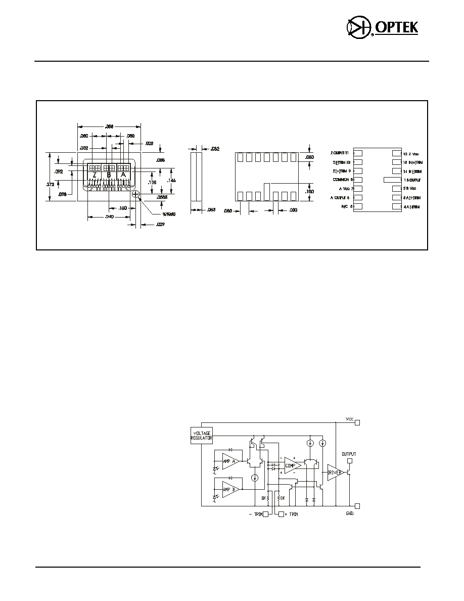
The OPR5011 is a hybrid sensor array
consisting of three channels of the Optek
OPC8332 Differential Optical
Comparator, ("TRI-DOC") IC. The single
chip construction ensures very tight
dimensional tolerances between active
areas. Specifically designed for
high-speed/high resolution encoder
applications, the open collector output
switches based on the comparison of
input photodiode's light current levels.
Logarithmic amplification of the input
signals makes possible operation over a
wide range of light levels.
The packages are surface mountable
and made from a custom opaque
polyimide which shields the active
devices from stray light. The high
temperature laminate can withstand
multiple exposures to the most
demanding soldering conditions. Wrap
around contacts are gold plated for
exceptional storage and wetting
characteristics.
Ab so lute Maxi mum Rat ings (T
A
= 25
o
C un less oth er wise noted)
Stor age Tem per a ture . . . . . . . . . . . . . . . . . . . . . . . . . . . . . . . . . . . . -40
∞
C to +100
∞
C
Op er ating Tem per a ture . . . . . . . . . . . . . . . . . . . . . . . . . . . . . . . . . . . -40
∞
C to +100
∞
C
Sup ply Volt age . . . . . . . . . . . . . . . . . . . . . . . . . . . . . . . . . . . . . . . . . . . . . . . . . . . . 24 V
Out put Volt age . . . . . . . . . . . . . . . . . . . . . . . . . . . . . . . . . . . . . . . . . . . . . . . . . . . . 24 V
Out put Cur rent . . . . . . . . . . . . . . . . . . . . . . . . . . . . . . . . . . . . . . . . . . . . . . . . . . `14 mA
Power Dis si pa tion. . . . . . . . . . . . . . . . . . . . . . . . . . . . . . . . . . . . . . . . . . . . . . . 500 mW
Sol dering Tem per a ture (Va por Phase Reflow for 30 sec onds) . . . . . . . . . . . . . 235
∞
C
Re places
OPR5003B
OPR5010
Prod uct Bul le tin OPR5011
Sep tem ber 2001
Op ti cal Com para tor Array
Type OPR5011
Optek Tech nol ogy, Inc. 1215 W. Crosby Road Carrollton, Texas 75006 (972) 323-2200 Fax (972) 323-2396
TBD
OPC8332 Block Di a gram
Type OPR5011
Op tek re serves the right to make changes at any time in or der to im prove de sign and to sup ply the best prod uct pos si ble.
Op tek Tech nol ogy, Inc. 1215 W. Crosby Road Car roll ton, Texas 75006 (972)323- 2200 Fax (972)323- 2396
Elec tri cal Char ac ter is tics (T
A
= 25
o
C un less oth er wise noted)
SYM BOL
PA RAME TER
MIN
TYP
MAX UNITS
TEST CON DI TIONS
NOTES
I
CC
Supply Current
9
20
mA
VCC = 24 V
V
OL
Low Level Output Voltage
0.3
0.4
V
I
OL
= 14 mA, VCC = 4.5 V
2
I
OH
High Level Output Current
0.1
1.0
µ
A
V
CC
= V
O
= 20.0 V
3
OPT-HYS Optical Hysteresis
40.0
%
V
CC
= 5.0 V, I
OL
= 1.0 mA
4, 7
OPT-OFF Optical Offset
-40
10
+40
%
V
CC
= 5.0 V, I
OL
= 1.0 mA
4, 7
f
max
Frequency Response
1.0
MHz
V
CC
= 5.0 V
5
t
lh
Output Rise Time
1.0
µ
s
6
t
hl
Output Fall Time
300
ns
NOTES:
1. Pin (+) = 1.2
µ
W and Pin (-) = 0.8
µ
W.
2. Pin (+) = 100.0 nW and Pin (-) = 1.0
µ
W.
3. Pin (+) = 1.0
µ
W and Pin (-) 100.0 nW.
4. Pin (-) held at 1.0
µ
W while Pin (+) is ramped from 0.5
µ
W to 1.5
µ
W and back to 0.5
µ
W.
5. Pin (+) mod u lated from 1.0
µ
W to 2.0
µ
W. Pin (-) mod u lated from 1.0
µ
W to 2.0
µ
W with phase shifted 180
∞
with re spect to Pin (+). Use 100 k
trimpot to set the out put sig nal to 50% duty cy cle for max i mum op er at ing fre quency.
6. Mea sured be tween 10% and 90% ponts.
7. Op ti cal Hys ter esis and Op ti cal Off set are found by plac i ng 1.0
µ
W of light on the in vert ing photodiode and ramping the light in ten sity of the
noninverting in put from .5
µ
W up to 1.5
µ
W and back down. This will pro duce two trig ger points, an up per trig ger point and lower trig ger point.
These points are used to cal cu late the op ti cal hysteresis and off set.
These are de fined as:
% Op ti cal Hys ter esis = 100 x (P rise - P fall)
P in (-)
% Op ti cal Off set = 100 x (P av er age -P (-) )
P in (-)
Where:
P in (-) = Light level in ci dent upon the "-" photodiode on the IC chip (Pin (-) = 1.0
µ
W).
P rise = Value of light power level in ci dent upon the "+" photodiode that is re quired to switch the dig i tal out put when the light level is an in creas ing
level (ris ing edge).
P fall = Value of light power level in ci dent upon the "+" photodiode that is re quired to switch the dig i tal out put when the light level is a de creas ing
level (fall ing edge).
P av er age = (P rise + P fall )
2
NOTES:
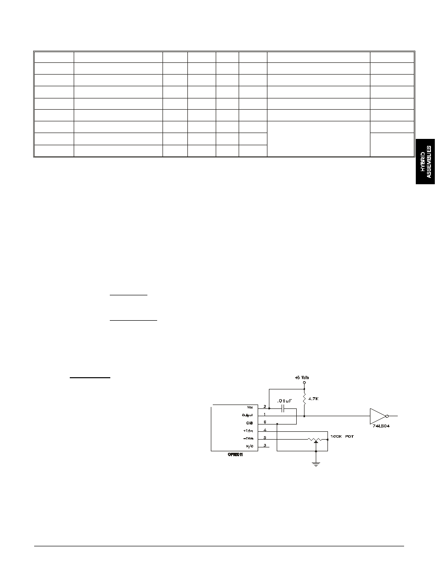
1. The 74LS04 is rec om mended as a means of iso lat ing the "DOC" com para tor cir cuitry from tran sients in duced by in duc tive and ca pac i tive loads.
2. It is rec om mended that a de coup ling ca pac i tor be placed as close as pos si ble to the de vice.
TBD
Ap pli ca tion Cir cuit