T-51382D064J-FW-P-AB (AB) No. 2002-0158
OPTREX CORPORATION
Page 1/20
LCD Module Technical Specification
T-51382D064J-FW-P-AB
NO.
ITEM
PAGE
-
Contents
1
1
Application
2
2
Features
2
3
Mechanical Specifications
2
4
Mechanical Drawing of TFT-LCD module
3
5
Input / Output Terminals
5
6
Absolute Maximum Ratings
6
7
Electrical Characteristics
6
8
Power On Sequence
12
9
Optical Characteristics
13
10
Handling Cautions
16
11
Reliability Test
17
12
Indication of Lot Number Label
17
13
Block Diagram
18
14
Packing Diagram
19
-
Revision History
20
Checked by (ACI Engineering Div.)
Checked by (Quality Assurance Div.)
Approved by (Production Div.)
Prepared by (Production Div.)
Type No.
Aug 12, 2002
O P T R E X
First Edition
Final Revision
******

T-51382D064J-FW-P-AB (AB) No. 2002-0158
OPTREX CORPORATION
Page 2/20
1. Application
This product applies computer peripheral, industrial meter, image communication,
web-pad, e-boobs and multi-media.
2. Features
. Pixel in stripe configuration
. Slim and compact
. Display Colors : 262,144 colors
. Viewing Direction : 6 o'clock
. Slim module design for mobile electronics device application
3. Mechanical Specifications
Parameter
Specifications
Unit
Screen Size
6.4 (diagonal)
inch
Display Format
640
�
R, G, B
�
480
dot
Active Area
129.6(H)
�
97.44 (V)
mm
Dot Pitch
0.0675 (H)
�
0.203 (V)
mm
Pixel Pitch
0.203 (H)
�
0.203 (V)
mm
Pixel Configuration
Stripe
Outline Dimension
See Mechanical Drawing
mm
Weight
165�10
g

T-51382D064J-FW-P-AB (AB) No. 2002-0158
OPTREX CORPORATION
Page 3/20
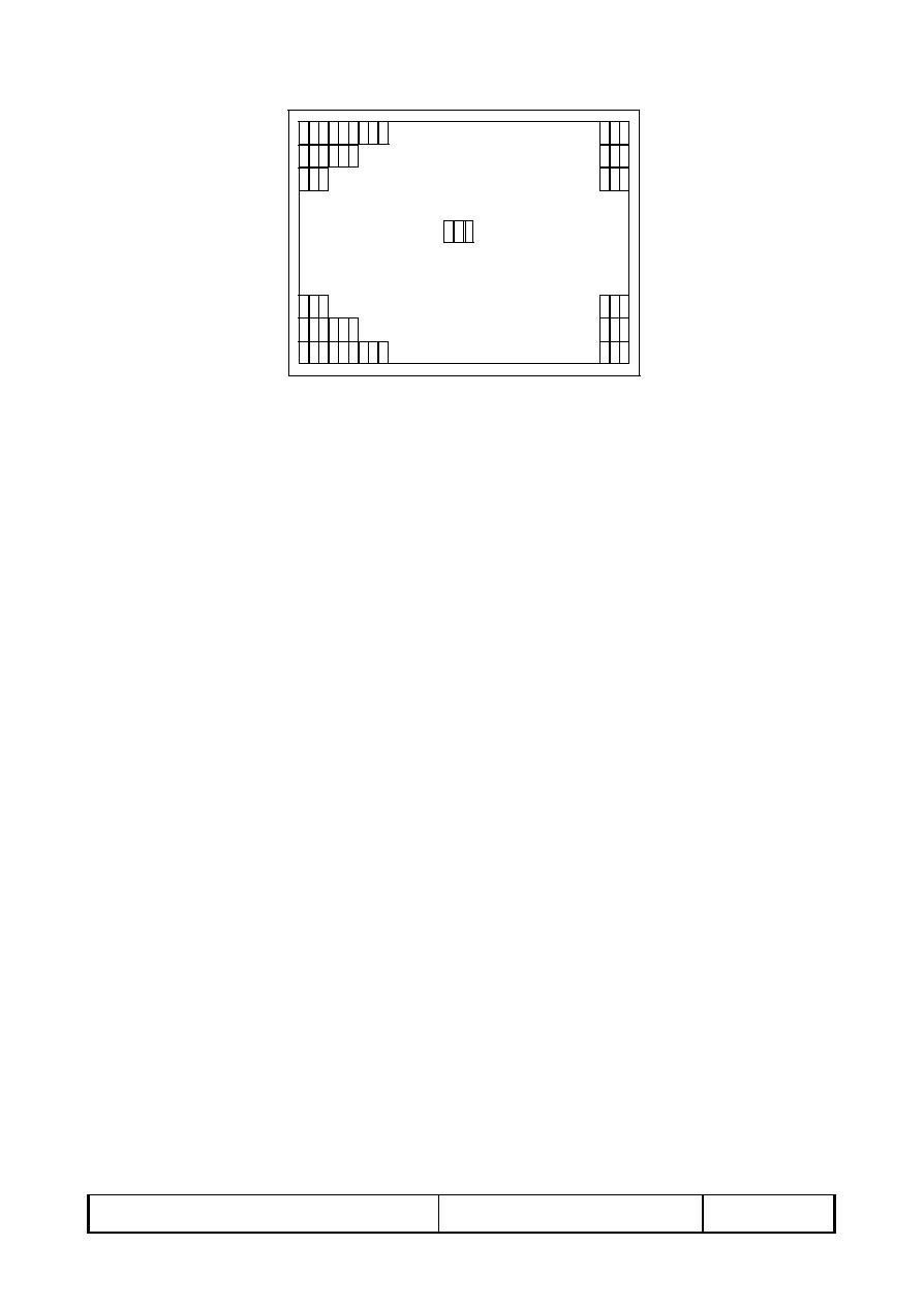
4.Mechanical Drawing of TFT-LCD Module
?
?
20
02.

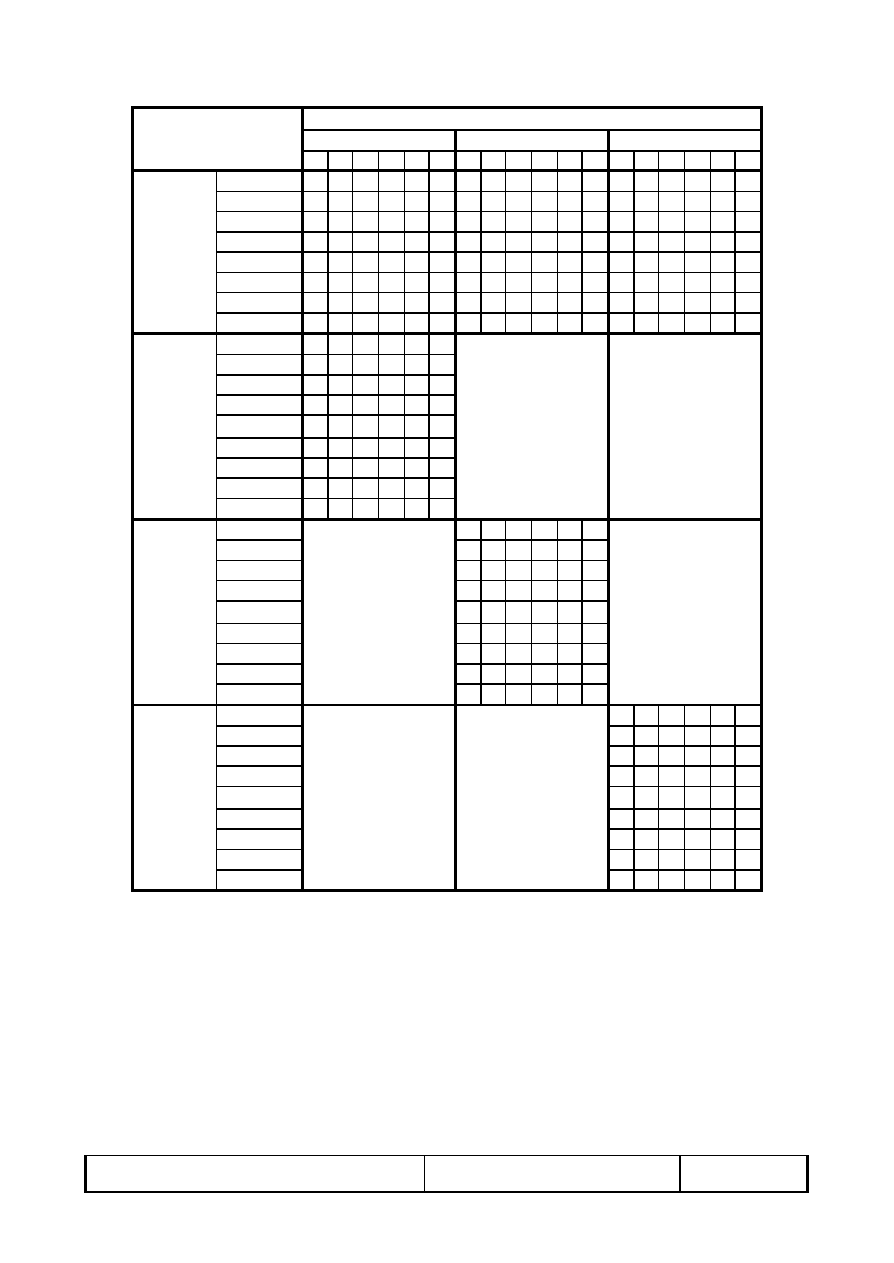
T-51382D064J-FW-P-AB (AB) No. 2002-0158
OPTREX CORPORATION
Page 4/20
?
?
20
02.
T-51382D064J-FW-P-AB (AB) No. 2002-0158
OPTREX CORPORATION
Page 5/20
5.Input / Output Terminals
5-1) TFT-LCD Panel Driving
Connector (1) type : ELCO , 6210-30PIN
Pin No.
Symbol
Function
Remark
1
CLK
Clock Signal for Sampling Image Digital Data
2
Hsync
Horizontal Synchronous Signal
3
Vsync
Vertical Synchronous Signal
4
GND
Ground (0V)
5
R0
Red Image Data Signal (LSB)
6
R1
Red Image Data Signal
7
R2
Red Image Data Signal
8
R3
Red Image Data Signal
9
R4
Red Image Data Signal
10
R5
Red Image Data Signal (MSB)
11
GND
Ground (0V)
12
G0
Green Image Data Signal (LSB)
13
G1
Green Image Data Signal
14
G2
Green Image Data Signal
15
G3
Green Image Data Signal
16
G4
Green Image Data Signal
17
G5
Green Image Data Signal (MSB)
18
GND
Ground (0V)
19
B0
Blue Image Data Signal (LSB)
20
B1
Blue Image Data Signal
21
B2
Blue Image Data Signal
22
B3
Blue Image Data Signal
23
B4
Blue Image Data Signal
24
B5
Blue Image Data Signal (MSB)
25
GND
Ground (0V)
26
NC
No connection
27
VCC
DC +3.3V Power Supply
28
VCC
DC +3.3V Power Supply
29
NC
No connection
30
NC
No connection
5-2) Backlight driving
Pin No
Symbol
Description
Remark
1
VL1
Input terminal (Hi voltage side)
Wire color : Pink
2
NC
No Connection
3
VL2
Input terminal (Low voltage side)
Wire Color : White
Note 5-1
Note 5-1 : Low voltage side of backlight inverter connects with ground of inverter circuits.

T-51382D064J-FW-P-AB (AB) No. 2002-0158
OPTREX CORPORATION
Page 6/20
5-3) Input / Output Connector
A) LCD module connector
ELCO , 6210-30PIN
Down Connector
Pin No. : 30
Pitch : 0.5 mm
B) Backlight Connector
JST BHR-03VS-1
Pin No. : 3
Pitch : 4 mm
Red: High Voltage
White: Low Voltage
6.Absolute Maximum Ratings:
GND=0V, Ta=25
�
C
Parameters
Symbol
MIN.
MAX.
Unit
Remark
+3.3V Supply Voltage
V
CC
-0.3
+4.0
V
Input Signals Voltage
V
sig
-0.3
V
CC
+0.3
V
Note 6-1
Storage Temperature
T
stg
-20
+70
�
C
Note 6-2
Operating Temperature
T
opa
-0
+60
�
C
Note 6-1: Input signals include CLK, Hsync, Vsync, R[0:5], G[0:5] and B[0:5].
Note 6-2: Humidity: 95% RH Max. at Ta
40
�
C.
Maximum wet-bulb temperature is at 39
�
C or less at Ta > 40
�
C.
No condensation.
7. Electrical Characteristics
7-1) Recommended Operating Conditions:
A) Driving for TFT-LCD panel
GND = 0V, Ta = 25
�
C
Parameters
Symbol
Min.
Typ.
Max.
Unit
Remark
+3.3V
Supply Voltage
V
CC
+3.15
+3.3
+3.6
V
Supply Input Ripple Voltage
V
CCRP
0.1
Vp-p
V
CC
=+3.3V
Input Signals Voltage (High)
V
IH
+3.0
+3.3
+3.6
V
Input Signals Voltage (Low)
V
IL
-
0
+0.3
V
B) Driving for backlight
Ta = 25
�
C
Item
Symbol
Min.
Typ.
Max.
Unit
Remark
Lamp Current
I
L
3
5
7
mA
Lamp Voltage
V
L
200
230
260
Vrms
Oscillation
P
L
45
64
80
KHz
Lamp Life Time
-
20,000
-
Hr
Kick-off voltage(25
�
C
)
Vs
-
845
1,050
Vrms
Kick-off voltage(0
�
C
)
Vs
-
1,045
1,250
Vrms
T-51382D064J-FW-P-AB (AB) No. 2002-0158
OPTREX CORPORATION
Page 7/20
7-2) Power Consumption
Parameters
Symbol
Typ.
Max.
Unit
Remark
+3.3V Current Dissipation
I
CC
170
200
mA
Input Signals Current (High)
I
IH
100
�
A
V
IH
=+3.3V
Input Signals Current (Low)
I
IL
100
�
A
V
IL
=0V
LCD Panel Power Consumption
0.56
0.66
W
Note 7-1
Backlight Power Consumption
1.95
2.10
W
Note 7-2
Note 7-1 : The power consumption of backlight is not included.
Note 7-2 : Backlight lamp power consumption is calculated by I
L
�
V
L
.
7-3) Input / Output signal timing chart
Parameters
Symbol
Min.
Typ.
Max.
Unit
Note
Frequency
Fc=1/Tc
25.175
MHz Note 7-3
Clock
High Time
Tckh
10
ns
Low Time
Tckl
10
ns
Periodic = Line
Thp
31.778
�
s
Note 7-3
Hsync
800
1024
clock Note 7-3
Pulse Width
Thpw
2
96
200
clock
Back Porch
Thbp
2
49
64
clock
515
525
1024
line
Note 7-3
Vsync
Pulse Width
Tvpw
1
2
line
Back Porch
Tvbp
1
33
64
line
Data
Setup Time
Tds
10
ns
Hold Time
Tdh
10
ns
Periodic = Line
Tep
800
1024
clock
Pulse Width (H)
Tepw
2
640
800
clock
Horizontal Display Periodic
Thd
640
640
640
clock
Hsync-CLK Phase Difference
Thc
10
Tc-10
ns
Vsync-Hsync Phase Difference
Tvh
1
Thp-1 clock
Note 7-3 : Tc is the period of sampling clock. In case of low-frequency, the image-flicker
may occur.

T-51382D064J-FW-P-AB (AB) No. 2002-0158
OPTREX CORPORATION
Page 8/20
7-4) Display Time Range
(1)
Vertical Timing :
(2)
Horizontal Timing :
Tvbp
Vsync
Hsync
Tvp
Tvpw
Vsync
(Negative)
(Positive)
Tvh
Hsync
Tds
Thp
Tc
Tckl
Tckh
Hsync
CLK
CLK
Thpw
Tep
Hsync
(Negative)
(Positive)
Thc
CLK
Tdh
R0~R5
G0~G5
B0~B5
Thbp
T-51382D064J-FW-P-AB (AB) No. 2002-0158
OPTREX CORPORATION
Page 9/20
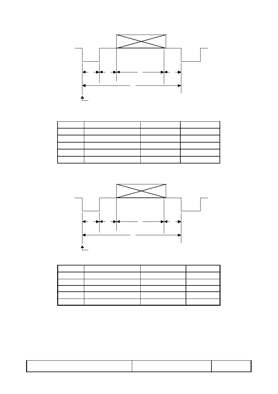
(3) Detail of Horizontal Timing :
Item
Description
Clock Cycles
Time
A
Horizontal Width
96
3.813
�
s
B
Horizontal B-Porch
49
1.907
�
s
C
Horizontal Display
640
25.422
�
s
D
Horizontal F-Porch
16
0.636
�
s
E
Horizontal Total
800
31.778
�
s
(4). Detail of Vertical Timing:
Item
Description
Horizontal Lines
Time
A
Vertical Width
2
63.5
�
s
B
Vertical B-Porch
33
1.049 ms
C
Vertical Display
480
15.253 ms
D
Vertical F-Porch
10
317.8
�
s
E
Vertical Total
525
16.683 ms
A
B
C
D
E
Reset Horizontal Counter to Zero
A
B
C
D
E
Reset Vertical Counter to Zero
T-51382D064J-FW-P-AB (AB) No. 2002-0158
OPTREX CORPORATION
Page 10/20
7-5) Pixel Arrangement
The LCD module pixel arrangement is the stripe.
R G B R G B R G B
R G B
R G B R G B
R G B
R G B R G B R G B
R G B
R G B R G B
R G B
3
rd Line
2 nd Line
1
st Line
480 th Line
479th Line
478 th Line
R G B
R G B
R G B
R G B
1 st Pixel
640 th Pixel
1 Pixel = R G B
T-51382D064J-FW-P-AB (AB) No. 2002-0158
OPTREX CORPORATION
Page 11/20
7-6) Display Color and Gray Scale Reference
Input Color Data
Color
Red
Green
Blue
R5 R4 R3 R2 R1 R0 G5 G4 G3 G2 G1 G0 B5 B4 B3 B2 B1 B0
Black
0 0 0 0 0 0 0 0 0 0 0 0 0 0 0 0 0 0
Red (63)
1 1 1 1 1 1 0 0 0 0 0 0 0 0 0 0 0 0
Green (63) 0 0 0 0 0 0 1 1 1 1 1 1 0 0 0 0 0 0
Basic
Blue (63)
0 0 0 0 0 0 0 0 0 0 0 0 1 1 1 1 1 1
Colors
Cyan
0 0 0 0 0 0 1 1 1 1 1 1 1 1 1 1 1 1
Magenta
1 1 1 1 1 1 0 0 0 0 0 0 1 1 1 1 1 1
Yellow
1 1 1 1 1 1 1 1 1 1 1 1 0 0 0 0 0 0
White
1 1 1 1 1 1 1 1 1 1 1 1 1 1 1 1 1 1
Red (00)
0 0 0 0 0 0 0 0 0 0 0 0 0 0 0 0 0 0
Red (01)
0 0 0 0 0 1 0 0 0 0 0 0 0 0 0 0 0 0
Red (02)
0 0 0 0 1 0 0 0 0 0 0 0 0 0 0 0 0 0
Darker
Red
Brighter
Red (61)
1 1 1 1 0 1 0 0 0 0 0 0 0 0 0 0 0 0
Red (62)
1 1 1 1 1 0 0 0 0 0 0 0 0 0 0 0 0 0
Red (63)
1 1 1 1 1 1 0 0 0 0 0 0 0 0 0 0 0 0
Green (00) 0 0 0 0 0 0 0 0 0 0 0 0 0 0 0 0 0 0
Green (01) 0 0 0 0 0 0 0 0 0 0 0 1 0 0 0 0 0 0
Green (02) 0 0 0 0 0 0 0 0 0 0 1 0 0 0 0 0 0 0
Darker
Green
Brighter
Green (61) 0 0 0 0 0 0 1 1 1 1 0 1 0 0 0 0 0 0
Green (62) 0 0 0 0 0 0 1 1 1 1 1 0 0 0 0 0 0 0
Green (63) 0 0 0 0 0 0 1 1 1 1 1 1 0 0 0 0 0 0
Blue (00)
0 0 0 0 0 0 0 0 0 0 0 0 0 0 0 0 0 0
Blue (01)
0 0 0 0 0 0 0 0 0 0 0 0 0 0 0 0 0 1
Blue (02)
0 0 0 0 0 0 0 0 0 0 0 0 0 0 0 0 1 0
Darker
Blue
Brighter
Blue (61)
0 0 0 0 0 0 0 0 0 0 0 0 1 1 1 1 0 1
Blue (62)
0 0 0 0 0 0 0 0 0 0 0 0 1 1 1 1 1 0
Blue (63)
0 0 0 0 0 0 0 0 0 0 0 0 1 1 1 1 1 1

T-51382D064J-FW-P-AB (AB) No. 2002-0158
OPTREX CORPORATION
Page 12/20
8. Power On Sequence
1. The supply voltage for input signals should be same as V
CC.
2. When the power is off , please keep whole signals (Hsync, Vsync, CLK, Data) low level
or high impedance
3.0 V
3.0 V
0 s< t <35 ms
0 s< t <35 ms
35ms
0<17ms
Signal
Backlight
V
CC
T-51382D064J-FW-P-AB (AB) No. 2002-0158
OPTREX CORPORATION
Page 13/20
9. Optical Characteristics
Ta=25
�
C
Parameter
Symbol Condition
MIN.
TYP. MAX. Unit
Remarks
Horizontal
�35
�45
deg
Note 9-3
(to 12
o'clock)
10
15
-
deg
Viewing
Angle
Vertical
(to 6
o'clock)
CR>10
30
35
-
deg
Contrast Ratio
CR
150
180
-
-
Note 9-1
Rise
Tr
-
15
30
ms
Response time
Fall
Tf
=0
�
-
25
50
ms
Note 9-4
Brightness
=0
�
/
=0
120
150
cd/m
2
Note 9-2
Luminance Uniformity
U
55
80
-
%
Note 9-6
Lamp Life Time
-
20,000
-
hr
x
0.230
0.280 0.330
-
White Chromaticity
y
0.270
0.320 0.370
-
Cross Talk
=0
�
-
-
3
%
Note 9-5
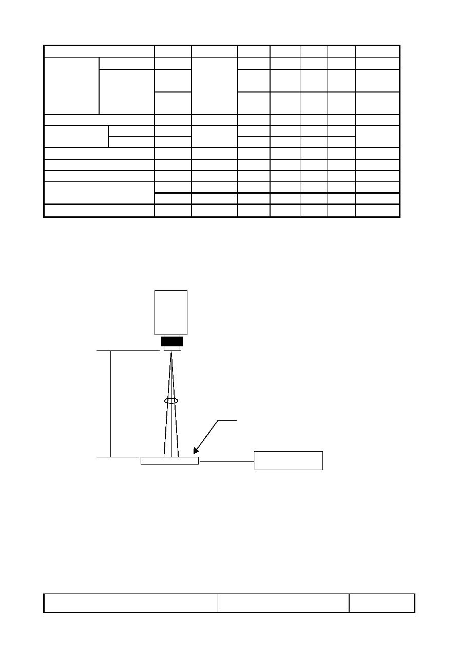
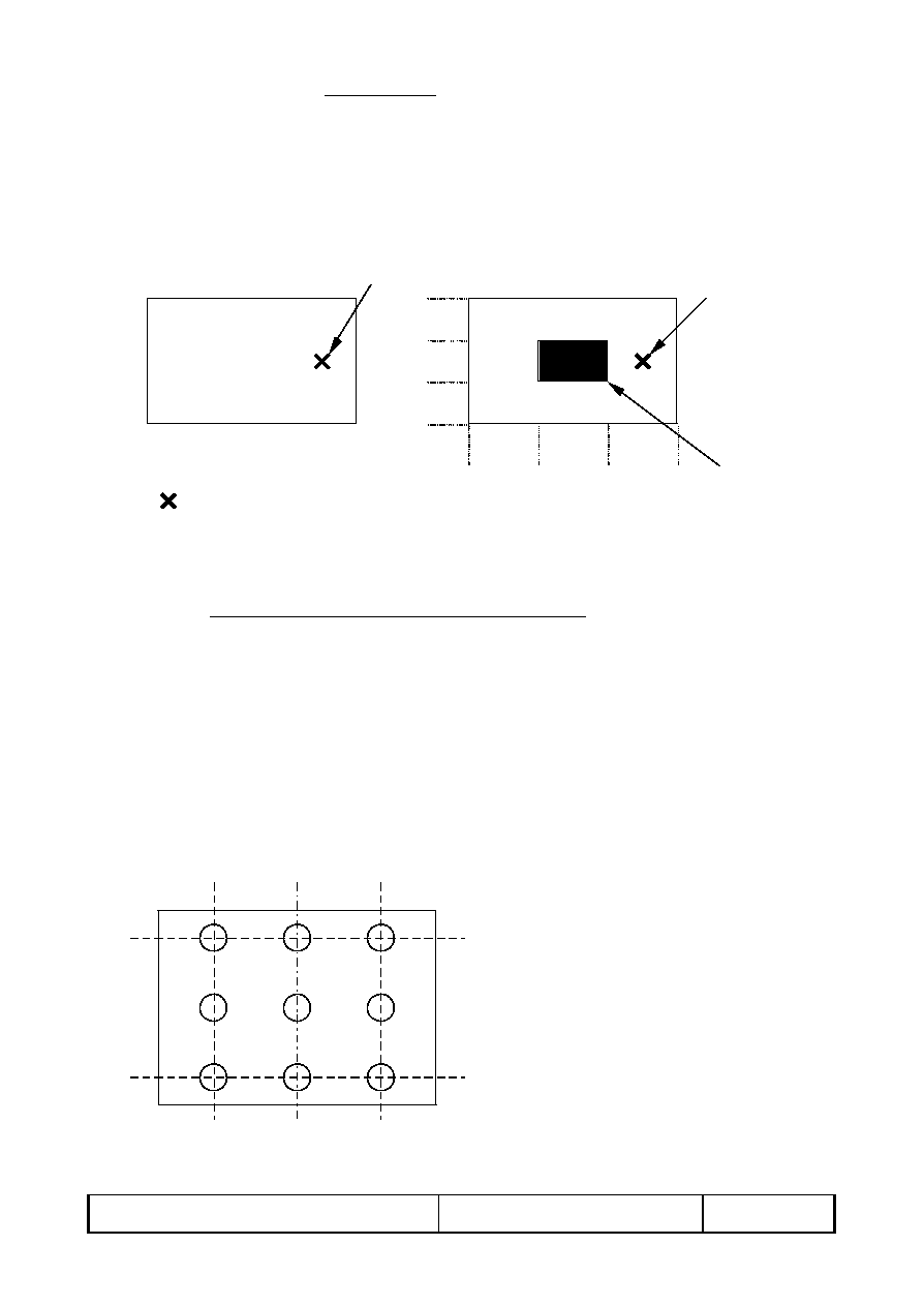
All the optical measurement shall be executed 30 minutes after backlight being turn-on. The optical
characteristics shall be measured in dark room (ambient illumination on panel surface less than 1
Lux). The measuring configuration shows as following figure.
Photometer (TOPCON
BM-5A or BM-7 fast)
500 mm +/- 50 mm
TFT-LCD module
DC/AC Inverter
Optical characteristics measuring configuration
Field = 2
�
T-51382D064J-FW-P-AB (AB) No. 2002-0158
OPTREX CORPORATION
Page 14/20
Luminance when LCD is White
Note 9-1:CR =
Luminance when LCD is Black
Contrast Ratio is measured in optimum common electrode voltage.
Note 9-2:Topcon BM-7(fast) luminance meter 2
�
field of view is used in the testing (after 20~30
minutes' operation).
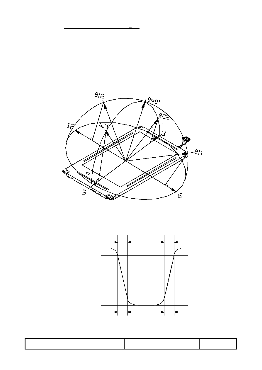
Note 9-3:The definitions of viewing angle diagrams :
Note 9-4: Definition of Response Time T
r
and T
f
:
100%
90%
10%
0%
White
White
B
r
i
g
h
t
n
e
s
s
Black
Tr
Tf
T-51382D064J-FW-P-AB (AB) No. 2002-0158
OPTREX CORPORATION
Page 15/20
YA-YB
Note 9-5 : Cross Talk (CTK) =
YA
�
100%
YA: Brightness of Pattern A
YB: Brightness of Pattern B
Pattern A
(Gray Level 31)
Pattern B
(Gray Level 31, central
black box exclusive)
: Testing Point (A and B are at the same point.)
YA
YB
1/3
1/3
1/3
1/3
1/3
1/3
Black
(Gray Level 0)
Note 9-6: The uniformity of LCD is defined as
The Minimum Brightness of the 9 testing Points
U =
The Maximum Brightness of the 9 testing Points
Luminance meter : BM-5A or BM-7 fast(TOPCON)
Measurement distance : 500 mm +/- 50 mm
Ambient illumination : < 1 Lux
Measuring direction : Perpendicular to the surface of module
The test pattern is white (Gray Level 63).
25%
50%
75%
25%
50%
75%

T-51382D064J-FW-P-AB (AB) No. 2002-0158
OPTREX CORPORATION
Page 16/20
10. Handling Cautions
10-1) Mounting of module
a) Please power off the module when you connect the input/output connector.
b) Please connect the ground pattern of the inverter circuit surely. If the connection
is not perfect, some following problems may happen possibly.
1.The noise from the backlight unit will increase.
2.The output from inverter circuit will be unstable.
3.In some cases a part of module will heat.
c) Polarizer which is made of soft material and susceptible to flaw must be
handled carefully.
d) Protective film (Laminator) is applied on surface to protect it against scratches
and dirts. It is recommended to peel off the laminator before use and taking
care of static electricity.
10-2) Precautions in mounting
a) When metal part of the TFT-LCD module (shielding lid and rear case) is soiled,
wipe it with soft dry cloth.
b) Wipe off water drops or finger grease immediately. Long contact with water may
cause discoloration or spots.
c) TFT-LCD module uses glass which breaks or cracks easily if dropped or bumped
on hard surface. Please handle with care.
d) Since CMOS LSI is used in the module. So take care of static electricity and
earth yourself when handling.
10-3) Adjusting module
a) Adjusting volumes on the rear face of the module have been set optimally before
shipment.
b) Therefore, do not change any adjusted values. If adjusted values are changed, the
specifications described may not be satisfied.
10-4) Others
a) Do not expose the module to direct sunlight or intensive ultraviolet rays for many
hours.
b) Store the module at a room temperature place.
c) The voltage of beginning electric discharge may over the normal voltage because of
leakage current from approach conductor by to draw lump read lead line around.
d) If LCD panel breaks, it is possibly that the liquid crystal escapes from the panel.
Avoid putting it into eyes or mouth. When liquid crystal sticks on hands, clothes or
feet. Wash it out immediately with soap.
e) Observe all other precautionary requirements in handling general electronic
components.
f) Please adjust the voltage of common electrode as material of attachment by 1
module.
T-51382D064J-FW-P-AB (AB) No. 2002-0158
OPTREX CORPORATION
Page 17/20
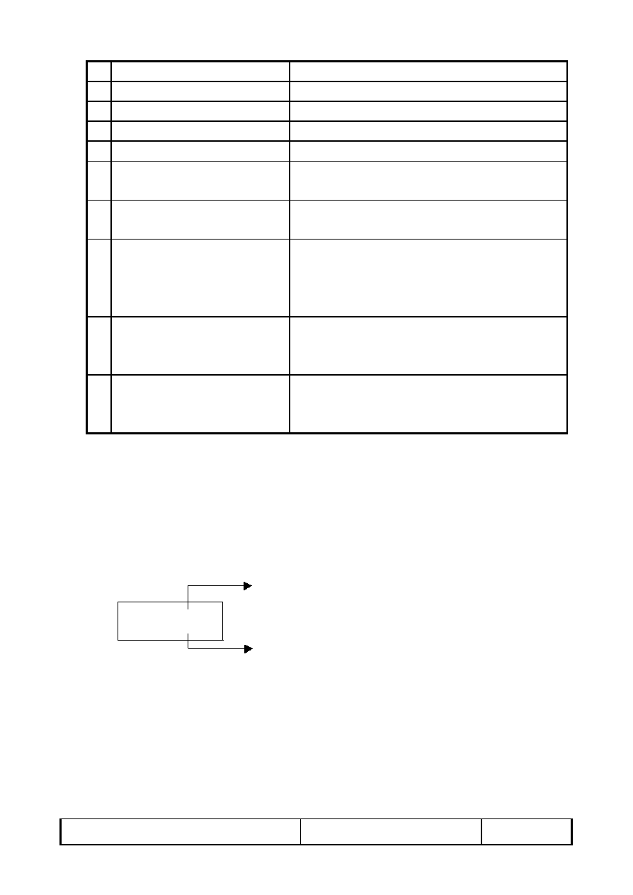
11. Reliability Test
No
Test Item
Test Condition
1
High Temperature Storage Test
Ta = +70
�
C, 240 hrs
2
Low Temperature Storage Test
Ta = -20
�
C, 240 hrs
3 High Temperature Operation Test
Ta = +60
�
C, 240 hrs
4 Low Temperature Operation Test
Ta = 0
�
C, 240 hrs
5
High Temperature & High
Humidity Operation Test
Ta = +40
�
C, 95%RH, 240 hrs
6
Thermal Cycling Test
(non-operating))
-25
�
C
+25
�
C
+70
�
C,200 Cycles
30 min 5min 30min
7
Vibration Test
(non-operating)
Frequency:10 ~ 57 H
Z
/Vibration Width :0.075mm
58-500 H
Z
/ Gravity :9.8m/s�
Sweep time: 11 minutes
Test period: 3 hrs for each direction of X, Y, Z
8
Shock Test
(non-operating)
Gravity :490m/s�
Direction:
�
X,
�
Y,
�
Z
Pulse Width :11ms,half sine wave
9
Electrostatic Discharge Test
(non-operating)
150pF,330
Air :
�
15KV:Contact :
�
8KV
10 times/point,9 point/panel face
Ta: ambient temperature
[Judgement Criteria]
Under the display quality test conditions with normal operation state , there should be no
change which may affect practical display function.
12. Indication of Lot Number Label
a) Indicated contents of the label
Lot number
Module number
Contents of lot number: 1st--Process area: class 1000
H
class 100K
M
2nd~3rd--Module screen size(in inch) : 1.8"
18, 2.5"
25......
5th--Production year: 1999
9, 2000
A, 2001
1........
6th--Production month: 1, 2, 3,....9, A, B, C
7th~10th--Serial numbers: 0001~9999
OOO-
OOOOOO
OD064VT2XX

T-51382D064J-FW-P-AB (AB) No. 2002-0158
OPTREX CORPORATION
Page 18/20
13. Block Diagram
1
2
3
4 7 9
4 7 8
4 8 0
1 2 3
1 9 2 0
Control Board
H
S Y N C
V
S Y N C
C L K
R[5:0]
G[5:0]
B[5:0]
I C V 1
IC V2
I C V 3
I C V 4
I C V 5
IC H1
IC H2
T F T - L C D
Display Area
Backlight
V
L
G N D
T-51382D064J-FW-P-AB (AB) No. 2002-0158
OPTREX CORPORATION
Page 19/20
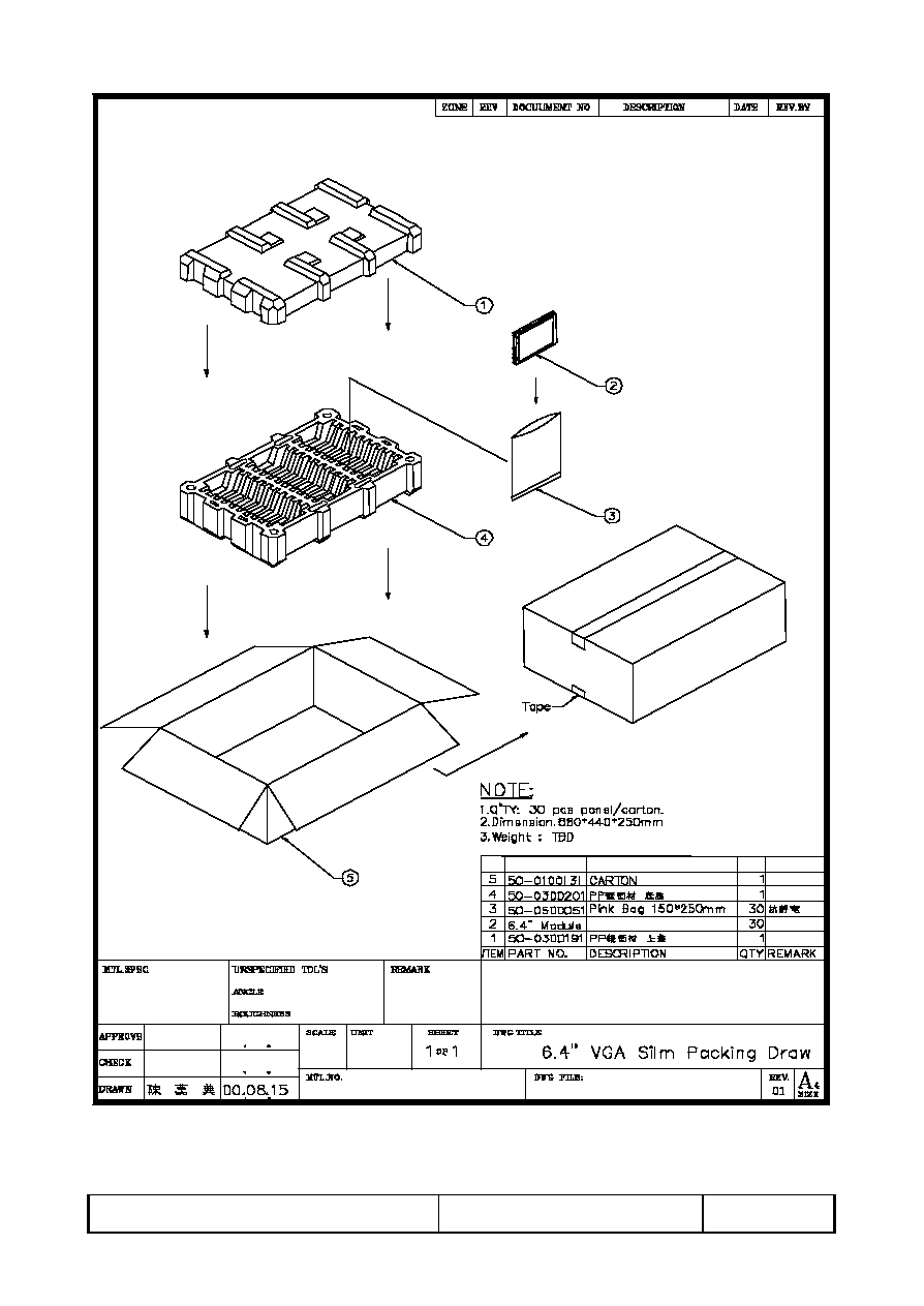
14. Packing Diagram
T-51382D064J-FW-P-AB (AB) No. 2002-0158
OPTREX CORPORATION
Page 20/20
Revision History
Rev.
Issued Date
Revised Contents
1.0
Mar. 27, 2002
NEW
1.1
Apr. 11, 2002
Modify
Page 5 : Driving for backlight
Page 7 : Power Consumption
Page 13 : Optical Characteristics (Brightness)