
OPTREX CORPORATION
T-51410D104-FW-P-AG
Page 1/18
LCD Module Technical Specification
T-51410D104-FW-P-AG
***The part number and specification are still tentative.
Table of Contents
1. Applications
.................................................................................................................................................
2
2. Features
...........................................................................................................................................................
2
3. Mechanical Specifications
................................................................................................................
2
4. Mechanical Drawing TFT LCD Module
............................................................................
3
5. Input / Output Terminals
.................................................................................................................
6
6. Absolute Maximum Ratings
............................................................................................................
7
7. Electrical Characteristics
.....................................................................................................................
7
8. Power Sequence
....................................................................................................................................
13
9. Optical Characteristics
.....................................................................................................................
14
10. Reliability TEST
....................................................................................................................................
17
11. Block Diagram
.........................................................................................................................................
18
Checked by (Design Engineering Div.)
Checked by (Quality Assurance Div.)
Prepared by (Production Div.)
Revision History
Rev.
Date
Page
Comment
First Edition
Mar. 28, 2002
Final Revision
******
O P T R E X
OPTREX CORPORATION
T-51410D104-FW-P-AG
Page 2/18
1.Application
This data sheet applies to a color TFT LCD module.
Module applies to OA product, car TV(must use Analog to Digital drive board), which
require high quality flat panel display. If you must use in high reliability environment can't over
reliability test condition
Optrex assumes no responsibility for any damage resulting from the use of the device
which dose not comply with the instructions and the precautions inthese specification sheet.
2. Features
. Amorphous silicon TFT LCD panel with back-light unit
. Pixel in stripe configuration
. Slim and compact, designed for O/A application
. Display Colors
262,144 colors
. Optimum Viewing Direction
12 o'clock
. 3.3V LVDS interface standard: DS90CF364 as receiver
. +3.3V DC supply voltage for TFT LCD panel driving
. Backlight driving DC/AC inverter not included in this module
. Wide Viewing Angle
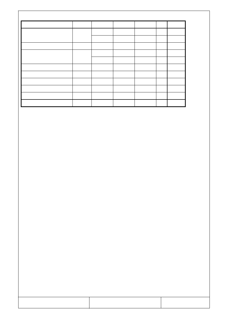
3.Mechanical Specifications
Parameter
Specifications
Unit
Screen Size
26.4(diagonal)
cm
10.4 (diagonal)
inch
Display Format
800
�
(R, G, B)
�
600
dot
Display Colors
262,144
Active Area
211.2(H)
�
158.4 (V)
mm
Pixel Pitch
0.264 (H)
�
0.264 (V)
mm
Pixel Configuration
Stripe
Outline Dimension
243 (w)
�
185.1(H)
�
11(typ.) (D)
mm
Weight
470(typ.),
g
Back-light
CCFL, 2 tubes
Surface treatment
Anti-glare and hard-coating
Display mode
Normally white

OPTREX CORPORATION
T-51410D104-FW-P-AG
Page 3/18
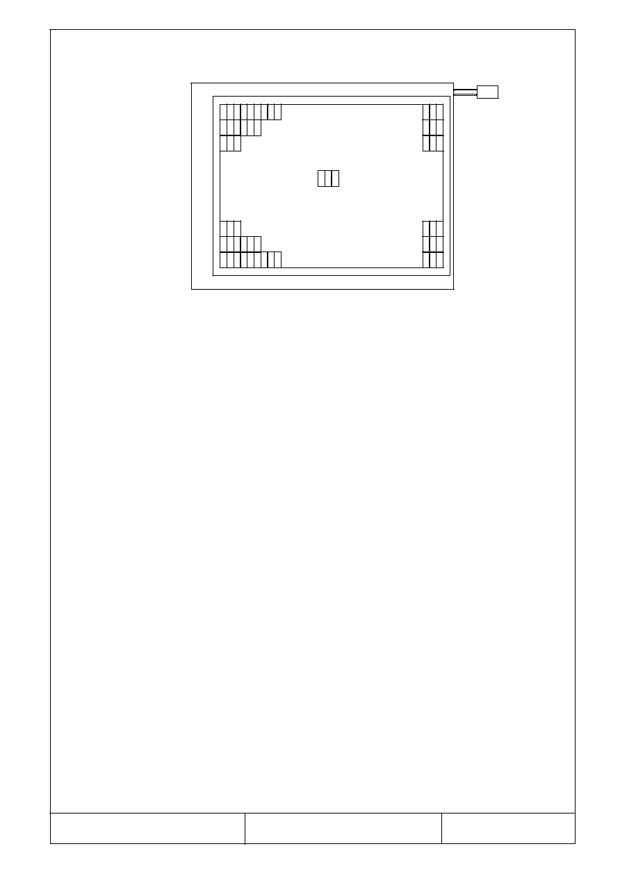
4.Mechanical Drawing of TFT-LCD Module
Unit: mm

OPTREX CORPORATION
T-51410D104-FW-P-AG
Page 4/18
OPTREX CORPORATION
T-51410D104-FW-P-AG
Page 5/18
5.Input Terminals
5-1) TFT-LCD Panel Driving
Connector type: Molex 55177-1491
Pin No.
Symbol
Function
Remark
1
VDD
Power supply : +3.3V
2
VDD
Power supply : +3.3V
3
GND
4
GND
5
IN0-
Pixel data Transmission pair 0 (negative -)
6
IN0+
Pixel data Transmission pair 0 (positive +)
7
IN1-
Pixel data Transmission pair 1 (negative -)
8
IN1+
Pixel data Transmission pair 1 (positive +)
9
IN2-
Pixel data Transmission pair 2 (negative -)
10
IN2+
Pixel data Transmission pair 2 (positive +)
11
CLK-
Sampling Clock (negative -)
12
CLK+
Sampling Clock (positive +)
13
GND
14
GND
Recommended Transmitter (DS90C*363 of National Semiconductor) to interface
Assignment:
Input
of DS
terminal
90C*363
Graphic controller output signal
Output signal
symbol
To interface
terminal(Symbol)
Symbol
No.
Symbol
Function
TIN0
44
R0
Red pixel data (LSB)
TIN1
45
R1
Red pixel data
TIN2
47
R2
Red pixel data
Tout0-
No.5 : IN0-
TIN3
48
R3
Red pixel data
TIN4
1
R4
Red pixel data
Tout0+
No.6 : IN0+
TIN5
3
R5
Red pixel data(MSB)
TIN6
4
G0
Green pixel data (LSB)
TIN7
6
G1
Green pixel data
TIN8
7
G2
Green pixel data
TIN9
9
G3
Green pixel data
Tout1-
No.7 : IN1-
TIN10
10
G4
Green pixel data
TIN11
12
G5
Green pixel data(MSB)
Tout1+
No.8 : IN1+
TIN12
13
B0
Blue pixel data(LSB)
TIN13
15
B1
Blue pixel data
TIN14
16
B2
Blue pixel data
TIN15
18
B3
Blue pixel data
TIN16
19
B4
Blue pixel data
Tout2-
No.9 : IN2-
TIN17
20
B5
Blue pixel data(MSB)
TIN18
22
NC
No connection
Tout2+
N0.10 : IN2+
TIN19
23
NC
No connection
TIN20
25
ENAB Compound Synchronization
signal
CLK in
26
NCLK Data sampling clock
TCLK out-
TCLK out+
No.11 : CLK IN-
No.12 : CLK IN+
OPTREX CORPORATION
T-51410D104-FW-P-AG
Page 6/18
Data stream of IN0-/+, IN1-/+ and IN2-/+
LVDS Interface Block Diagram
Gra
ph
i
c
C
o
n
t
ro
l
l
er
C
i
rcu
i
t
TIN0~TIN5
TIN6~TIN11
TIN12~TIN17
TIN18
TIN19
TIN20
TCLK IN
R0~R5
G0~G5
B0~B5
NC
NC
ENAB
CLK IN
TTL
pa
ral
l
el
t
o
L
VD
S
PLL
DS90C*363
L
V
DS
t
o
TTL
pa
ral
l
el
PLL
DS90CF364
IN0-
IN0+
RxOUT0~RxOUT5
RxOUT6~RxOUT11
RxOUT12~RxOUT17
RxOUT18
RxOUT19
RxOUT20
CLK OUT
L
C
D
In
t
ern
al
C
i
rcu
i
t
IN1-
IN1+
IN2-
IN2+
CLK-
CLK+
module side
Customer system side
5-2) Backlight driving
Connector type : "BHR-02VS-1" of
Japan Solderless Terminal MFG Co. LTD
PIN NO.
Symbol
Description
Remark
1
LV
Ground
White
2
HV
Lamp power input
Pink (or Gray)
3
HV
Lamp power input
Pink (or Gray)
RxOUT6 RxOUT5 RxOUT4
RxOUT3 RxOUT2 RxOUT1
RxOUT0
G0
R5
R4
R3
R2
R1
R0
IN0
RxOUT13 RxOUT12 RxOUT11 RxOUT10 RxOUT9 RxOUT8
RxOUT7
B1
B0
G5
G4
G3
G2
G1
IN1
RxOUT13 RxOUT12 RxOUT11 RxOUT10 RxOUT9 RxOUT8
RxOUT7
ENAB
NC
NC
B5
B4
B3
B2
IN2

OPTREX CORPORATION
T-51410D104-FW-P-AG
Page 7/18
6.Absolute Maximum Ratings:
GND=0V, Ta=25
Parameters
Symbol
MIN.
MAX.
Unit
Remark
Supply Voltage
V
DD
-0.3
+4.0
V
Input Signals Voltage
V
IN
-0.3
VDD+0.3
V
Note 6-1
Backlight Driving Voltage
V
L
-
2000
V
Backlight Driving Frequency
F
L
0
100
KHz
Storage Temperature
T
ST
-20
+60
Note 6-2
Operating Temperature
T
OP
0
+50
Note 6-1: LVDS signal
Note 6-2: Humidity : 80% RH Max. at Ta
�
40
.
Maximum wet-bulb temperature is at 39
or less at Ta > 40
and no
condensation.
7.Electrical Characteristics
7-1) Recommended Operating Conditions:
GND = 0V
Ta = 25
Item
Symbol
Min.
Typ.
Max.
Unit
Remark
Supply Voltage
VDD
3.0
3.3
3.6
V
Current Dissipation
I
DD
-
370
430
mA
Note 7-1
LVDS Differential input high threshold
V
TH
-
-
100
mV
Note 7-2
LVDS Differential input low threshold
V
TL
-100
-
-
Lamp Current
I
FL
6.0
14.0
16.0
mA
Note 7-3
Note 7-5
Lamp Voltage
V
L
400
430
530
Vrms
Note 7-3
Lamp Initial Voltage
V
SFL
-
-
875
Vrms
at Ta=25
�
C
Note 7-4
-
-
1300
at Ta=0
�
C
Note 7-4
Lamp Driving Frequency
F
L
30
55
60
KHz
Lamp power consumption
4
8
11
W
Note 7-5
Lamp Life Time
30000 40000
Hrs
Note 7-6
LCD Panel Life Time(MTBF)
50000
Hrs
Note 7-1 : To test the current dissipation of VDD, using the "color bars" testing pattern
shown as below
1
2
3
4
5
6
7
8
1.
White
2.
Yellow
3.
Cyan
4.
Green
5.
Magenta
6.
Red
7.
Blue
8.
Black
Idd current dissipation testing pattern

OPTREX CORPORATION
T-51410D104-FW-P-AG
Page 8/18
Note 7-2 : Please refers to DS90CF364 specification by National Semiconductor
Corporation.
This LCD module conforms to LVDS standard.
Note 7-3 : The back-light driving waveform should be as closed to sine-wave as possible.
In order to satisfy the quality of B/L , no matter use what kind of inverter , the
output lamp current must between Min. and Max. to avoid the abnormal
display image caused by B/L.
Note 7-4 : Not including the efficiency of backlight DC/AC inverter
Note 7-5 : Lamp current is measured with current meter for high frequency as shown below
Inverter
TFT-LCD
Module
~
A
* Pin 3 is V
low
** Current meter :
Yokogawa 2016-01
3
2
1
Note 7-6: The life time is determined as the time at which brightness of lamp is 50%
compare
to that of initial value at the typical lamp current.
7-2) Input / Output signal timing chart
(A) Vertical Timing
X,1
X,2
X,3 X,4
X,598 X,599 X,600
X,Y
t
1
t
2
t
3
t
3
CLK
ENAB
R5~R0
G5~G0
B5~B0
Lamp current dissipation testing configuration
OPTREX CORPORATION
T-51410D104-FW-P-AG
Page 9/18
(B) Horizontal Timing
t
3
t
4
t
c
CLK
ENAB
R5~R0
G5~G0
B5~B0
1,Y 2,Y 3,Y 4,Y 5,Y 6,Y 7,Y
X,Y
798,Y 800,Y
797,Y 799,Y
CLK
t 6
t 7
t 5
V
IH
(Min):0.8V
cc
V
IL
(Max):0.2V
cc
ENAB
R5-R0
G5-G0
B5-B0
VALID
DATA
Input Signal
CenterLevel:
0.5V
cc
V
IH
(Min):0.8V
cc
V
IL
(Max):0.2V
cc
CLK
a
b
0.5V
cc
Duty ( a ,b ) : 50 10%
t 8
t 9
OPTREX CORPORATION
T-51410D104-FW-P-AG
Page 10/18
D) Timing Specifications
Item
Symbol
Min.
Typ.
Max.
Unit Remark
Frame Cycling
t1
604 X t3
628X t3
660 X t3
-
-
16.58
17.86
ms
Vertical Display Period
t2
600 X t3
600 X t3
600 X t3
-
Horizontal Scanning Time
t3
844 X t5
1056 X t5 1064 X t5
-
26.3
26.4
-
s
Horizontal Display Period
t4
-
800 X t5
-
-
Clock Cycle
t5
24.0
25.0
-
ns
Clock High Level Time
t6
9.0
-
-
ns
Clock Low Level Time
t7
9.0
-
-
ns
Hold time
t8
4.0
-
-
ns
Set-up time
t9
5.0
-
-
ns

OPTREX CORPORATION
T-51410D104-FW-P-AG
Page 11/18
7-3) Display Color and Gray Scale Reference
Input Color Data
Color
Red
Green
Blue
R5 R4 R3 R2 R1 R0 G5 G4 G3 G2 G1 G0 B5 B4 B3 B2 B1 B0
Black
0
0
0
0
0
0
0
0
0
0
0
0
0
0
0
0
0
0
Red (63)
1
1
1
1
1
1
0
0
0
0
0
0
0
0
0
0
0
0
Green
(63)
0
0
0
0
0
0
1
1
1
1
1
1
0
0
0
0
0
0
Basic
Blue (63)
0
0
0
0
0
0
0
0
0
0
0
0
1
1
1
1
1
1
Colors
Cyan
0
0
0
0
0
0
1
1
1
1
1
1
1
1
1
1
1
1
Magenta
1
1
1
1
1
1
0
0
0
0
0
0
1
1
1
1
1
1
Yellow
1
1
1
1
1
1
1
1
1
1
1
1
0
0
0
0
0
0
White
1
1
1
1
1
1
1
1
1
1
1
1
1
1
1
1
1
1
Red (00)
0
0
0
0
0
0
0
0
0
0
0
0
0
0
0
0
0
0
Red (01)
0
0
0
0
0
1
0
0
0
0
0
0
0
0
0
0
0
0
Red (02)
0
0
0
0
1
0
0
0
0
0
0
0
0
0
0
0
0
0
Darker
Red
Brighter
Red (61)
1
1
1
1
0
1
0
0
0
0
0
0
0
0
0
0
0
0
Red (62)
1
1
1
1
1
0
0
0
0
0
0
0
0
0
0
0
0
0
Red (63)
1
1
1
1
1
1
0
0
0
0
0
0
0
0
0
0
0
0
Green
(00)
0
0
0
0
0
0
0
0
0
0
0
0
0
0
0
0
0
0
Green
(01)
0
0
0
0
0
0
0
0
0
0
0
1
0
0
0
0
0
0
Green
(02)
0
0
0
0
0
0
0
0
0
0
1
0
0
0
0
0
0
0
Darker
Green
Brighter
Green
(61)
0
0
0
0
0
0
1
1
1
1
0
1
0
0
0
0
0
0
Green
(62)
0
0
0
0
0
0
1
1
1
1
1
0
0
0
0
0
0
0
Green
(63)
0
0
0
0
0
0
1
1
1
1
1
1
0
0
0
0
0
0
Blue (00)
0
0
0
0
0
0
0
0
0
0
0
0
0
0
0
0
0
0
Blue (01)
0
0
0
0
0
0
0
0
0
0
0
0
0
0
0
0
0
1
Blue (02)
0
0
0
0
0
0
0
0
0
0
0
0
0
0
0
0
1
0
Darker
Blue
Brighter
Blue (61)
0
0
0
0
0
0
0
0
0
0
0
0
1
1
1
1
0
1
Blue (62)
0
0
0
0
0
0
0
0
0
0
0
0
1
1
1
1
1
0
Blue (63)
0
0
0
0
0
0
0
0
0
0
0
0
1
1
1
1
1
1
OPTREX CORPORATION
T-51410D104-FW-P-AG
Page 12/18
7-4) Pixel Arrangement
The LCD module pixel arrangement is the stripe.
R G B R G B R G B
R G B
R G B R G B
R G B
R G B R G B R G B
R G B
R G B R G B
R G B
3rd Line
2 nd Line
1st Line
600 th Line
599 th Line
598 th Line
R G B
R G B
R G B
R G B
1 st Pixel
800 th Pixel
1 Pixel = R G B

OPTREX CORPORATION
T-51410D104-FW-P-AG
Page 13/18
8.)Power On Sequence
1. The supply voltage for input signals should be same as V
CC.
2. When the power is off , please keep whole signals (Hsync, Vsync, CLK, Data) low level
or high impedance
3.0 V
3.0 V
0 s< t <35 ms
0 s< t <35 ms
2t
1
0<t
1
Signal
Backlight
V
CC
OPTREX CORPORATION
T-51410D104-FW-P-AG
Page 14/18
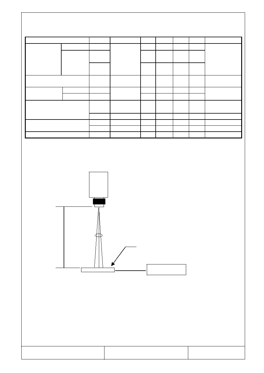
9.) Optical Characteristics
9-1) Specification:
Ta = 25
Parameter
Symbol
Condition
MIN.
TYP.
MAX.
Unit
Remarks
Horizontal
�
55
�
60
-
deg
(to 12
o'clock)
50
55
-
deg Note 9-1
Viewing Angle
Vertical
(to 6
o'clock)
CR
�
10
35
40
-
deg
Contrast Ratio
CR
Optimum
direction
100
180
-
-
Note 9-2
Rise
Tr
-
15
50
ms
Response time
Fall
Tf
=0
�
=0
�
-
25
50
ms
Note 9-4
Luminance
L
=0
�
/
=0
�
310
350
-
cd/
Note 9-3
Luminance Uniformity
U
55
80
-
%
Note 9-5
x
0.280 0.330 0.380
-
White Chromaticity
y
0.340 0.390 0.440
-
Cross Talk Ratio
CTK
-
-
3.5
%
Note 9-6
All the optical measurement shall be executed 30 minutes after backlight being turn-on. The
optical characteristics shall be measured in dark room (ambient illumination on panel surface
less than 1 Lux). The measuring configuration shows as following figure.
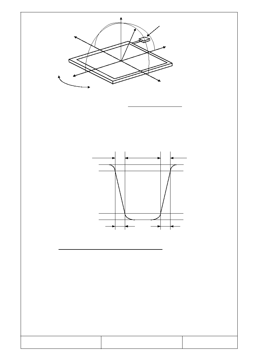
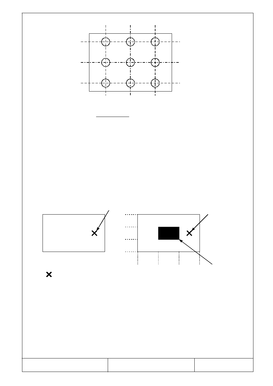
Note 9-1`
The definitions of viewing angles are as follows.
Photometer (TOPCON
BM-5A or BM-7 fast)
500
mm
+/-
50
mm
TFT-LCD module
DC/AC Inverter
Optical characteristics measuring configuration
Field = 2
�
OPTREX CORPORATION
T-51410D104-FW-P-AG
Page 15/18
12 o'clock
3 o'clock
9 o'clock
6 o'clock
q
f
Lamp connector
Note 9-2 : The definition of contrast ratio
CR
Luminance at gray level 63
Luminance at gray level 0
=
Note 9-3
Topcon BM-5A
luminance meter 2
�
field of view is used in the testing (after 30
minutes' operation). The typical luminance value is measured at lamp current 14.0
mA.
Note 9-4: Definition of Response Time T
r
and T
f
:
100%
90%
10%
0%
White
White
B
r
i
g
h
t
n
e
s
s
Black
Tr
Tf
Note 9-5: The uniformity of LCD is defined as
The Minimum Brightness of the 9 testing Points
U =
The Maximum Brightness of the 9 testing
Points
Luminance meter : BM-5A or BM-7 fast(TOPCON)
Measurement distance : 500 mm +/- 50 mm
Ambient illumination : < 1 Lux
Measuring direction : Perpendicular to the surface of module
The test pattern is white (Gray Level 63).
OPTREX CORPORATION
T-51410D104-FW-P-AG
Page 16/18
25%
50%
75%
25%
50%
75%
�
YA-YB
�
Note 8-6: Cross Talk (CTK) =
YA
�
100%
YA: Brightness of Pattern A
YB: Brightness of Pattern B
Luminance meter : BM 5A (TOPCON)
Measurement distance : 500 mm +/- 50 mm
Ambient illumination : < 1 Lux
Measuring direction : Perpendicular to the surface of module
Pattern A
(Gray Level 31)
Pattern B
(Gray Level 31, central
black box exclusive)
: Measuring Point (A and B are at the same point.)
YA
YB
1/3
1/3
1/3
1/3
1/3
1/3
Black
(Gray Level 0)
OPTREX CORPORATION
T-51410D104-FW-P-AG
Page 17/18
10. Reliability Test
No
Test
Item
Test
Condition
Remark
1
High Temperature Storage Test
Ta = +60
, 240 hrs
2
Low Temperature Storage Test
Ta = -20
, 240 hrs
3
Low Temperature Operation Test Ta = 0
, 240 hrs
4
High Temperature & High Humidity
Operation Test
Ta = +50
, 80%RH, 240 hrs
(No Condensation)
5
Thermal Cycling Test
(non-operating)
0
��
+25
��
+60
, 50 Cycles
1Hr
0.5Hr
1Hr
6
Vibration Test
(non-operating)
Frequency
10 ~ 57 H
Z ,
Amplitude
0.15 mm
58~500Hz, 1G
Sweep time: 11 min
Test Period: 3 hrs (1 hr for each direction of
X, Y, Z)
7
Shock Test
(non-operating)
80G, 6ms, X,Y, Z
1 times for each direction
Ta: ambient temperature
[Judgement Criteria]
Under the display quality test conditions with normal operation state , there should be no
change which may affect practical display function.
OPTREX CORPORATION
T-51410D104-FW-P-AG
Page 18/18
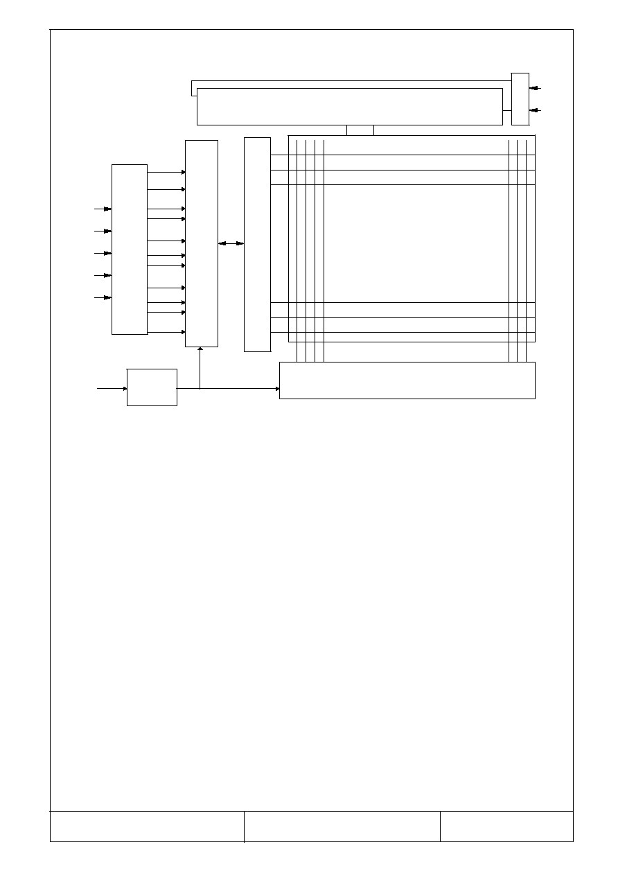
11.)Block Diagram
1
2
3
599
598
600
4
2
1
2400
C
o
n
t
r
o
l
C
i
r
c
u
i
t
E N A B
C LK
IN 0-/+
IN 1-/+
IN 2-/+
T F T -LC D
D isplay A rea
B a ck-ligh t(La m p1 )
V L1
V L2
3
S o u rce D rive r
G
a
t
e
D
r
i
v
e
r
L
V
D
S
I
n
t
e
r
f
a
c
e
(
D
S
9
0
C
3
6
4
)
Pow er
M odule
V D D
E N A B
C L K
R 0
R 1
G 0
G 11
B 0
B 1
R 5
G 5
B 5
...
...
...