 | –≠–ª–µ–∫—Ç—Ä–æ–Ω–Ω—ã–π –∫–æ–º–ø–æ–Ω–µ–Ω—Ç: HDSP2113S | –°–∫–∞—á–∞—Ç—å:  PDF PDF  ZIP ZIP |

2000 Infineon Technologies Corp. ∑ Optoelectronics Division ∑ San Jose, CA
www.infineon.com/opto ∑ 1-888-Infineon (1-888-463-4636)
OSRAM Opto Semiconductors GmbH & Co. OHG ∑ Regensburg, Germany
www.osram-os.com ∑ +49-941-202-7178
1
March 24, 2000-13
FEATURES
∑ Eight 0.200" Dot Matrix Characters in Red, Yellow,
High Efficiency Red, Green, High Efficiency Green,
or Soft Orange
∑ Built-in 128 Character ROM,
Mask Programmable for Custom Fonts
∑ Readable from 8 Feet (2.5 meters)
∑ Built-in Decoders, Multiplexers and Drivers
∑ Wide Viewing Angle, X Axis ±55
∞
, Y Axis ±65
∞
∑ Programmable Features:
≠ Individual Flashing Character
≠ Full Display Blinking
≠ Multi-Level Dimming and Blanking
≠ Clear Function
≠ Self Test
∑ Internal or External Clock
∑ End Stackable Dual-In-Line Plastic Package
∑ Read/Write Capability
∑ 16 User Definable Characters
DESCRIPTION
The HDSP2110S (Red), HDSP2111S (Yellow), HDSP2112S (High Effi-
ciency Red), HDSP2113S (Green), HDSP2114S (High Efficiency
Green), and HDSP2115S (Soft Orange) are eight digit, 5 x 7 dot matrix,
alphanumeric Intelligent Display devices. The 0.20 inch high digits are
packaged in a rugged, high quality, optically transparent, 0.6 inch lead
spacing, 28 pin plastic DIP.
The on-board CMOS has a built-in 128 character ROM. The
HDSP211XS also has a user definable character (UDC) feature, which
uses a RAM that permits storage of 16 arbitrary characters, symbols
or icons that are software-definable by the user. The character ROM
itself is mask programmable and easily modified by the manufacturer
to provide specified custom characters.
The HDSP211XS is designed for standard microprocessor interface
techniques, and is fully TTL compatible. The Clock I/O and Clock
Select pins allow the user to cascade multiple display modules.
1.680 (42.67) max.
0.210
(5.34)
0.105
(2.67)
0.386
(9.8)
0.771
(19.58)
0.600
(15.24)
0.086
(2.19)
0.012 (0.30) typ.
0.100
(2.54) typ.
0.018 typ.
(.46)
0.160
±
.020
(4.06
±
.50)
0.209 (5.31)
HDSP211X
OSRAM
WW
Z
1
Part Number
Pin 1 Indicator
EIA Date
Code
Intensity Code
Color Bin
(For Yellow Only)
0.189
(4.81)
0.189
(4.79)
Dimensions in inches (mm)
RED
HDSP2110S
YELLOW
HDSP2111S
HIGH EFFICIENCY RED
HDSP2112S
GREEN
HDSP2113S
HIGH EFFICIENCY GREEN
HDSP2114S
SOFT ORANGE
HDSP2115S
0.200" 8-Character 5x7 Dot Matrix Parallel Input
Alphanumeric Intelligent Display
Æ
Devices
2000 Infineon Technologies Corp. ∑ Optoelectronics Division ∑ San Jose, CA
HDSP2110S/1S/2S/3S/4S/5S
www.infineon.com/opto ∑ 1-888-Infineon (1-888-463-4636)
OSRAM Opto Semiconductors GmbH & Co. OHG ∑ Regensburg, Germany
www.osram-os.com ∑ +49-941-202-7178
2
March 24, 2000-13
Maximum Ratings
(
T
A
=25
∞
C)
DC Supply Voltage,
V
CC
to GND
(max. voltage with no LEDs on) ...................≠0.3 to +7.0 VDC
Input Voltage Levels,
All Inputs ....................................................... ≠0.3 to
V
CC
+0.3
Operating Temperature ....................................... ≠40
∞
C to 85
∞
C
Storage Temperature ......................................... ≠40
∞
C to 100
∞
C
Relative Humidity (non-condensing) ....................................85%
Operating Voltage,
V
CC
to GND
(Max. voltage with 20 dots/digits on).............................. 5.5 V
Maximum Solder Temperature
(0.063" below seating plane, t<5.0 s)............................ 260
∞
C
ESD Protection at 1.5 k
,
100 pF .....................................................V
Z
=4.0 kV (each pin)
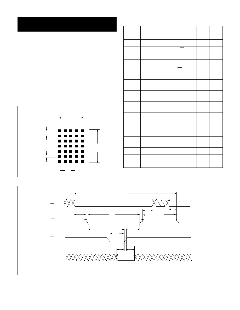
Figure 1. Enlarged Character Font
Figure 2. Write Cycle Timing Diagram
Input pulse levels ≠0.6 V to 2.4 V
ESD Warning:
Standard precautions for CMOS
handling should be observed.
0.112
(2.85)
0.030 (0.76) Typ.
0.01 (0.254)
0.026 (0.65) Typ.
0.189
(4.81)
R1
R2
R3
R4
R5
R6
R7
C1 C2 C3 C4 C5
Dimensions in inches (mm)
Tacc
Twd
Tdh
Tw
Tces
Tcer
Tceh
Tacs
Tach
Tacs
A0-A3
FL
Tce
CE
WR
D0-D7
Input pulse levels --0.6 V to 2.4 v
Switching Specifications
(over operating temperature range and
V
CC
=4.5 V)
Symbol
Description
Min.
Units
T
acc
Display Access Time--Write
210
ns
T
acc
Display Access Time--Read
230
ns
T
acs
Address Setup Time to CE
10
ns
T
ce
Chip Enable Active Time--Write
140
ns
T
ce
Chip Enable Active Time--Read
160
ns
T
ach
Address Hold Time to CE
20
ns
T
cer
Chip Enable Recovery Time
60
ns
T
ces
Chip Enable Active Prior to
Rising Edge--Write
140
ns
T
ces
Chip Enable Active Prior to
Rising Edge--Read
160
ns
T
ceh
Chip Enable Hold to Rising Edge
of Read/Write Signal
0
ns
T
w
Write Active Time
100
ns
T
wd
Data Valid Prior to
Rising Edge of Write Signal
50
ns
T
dh
Data Write Time
20
ns
T
r
Chip Enable Active Prior to Valid
Data
160
ns
T
rd
Read Active Prior to Valid Data
95
µ
s
T
df
Read Data Float Delay
10
ns
T
rc
Reset Active Time
300
ns
2000 Infineon Technologies Corp. ∑ Optoelectronics Division ∑ San Jose, CA
HDSP2110S/1S/2S/3S/4S/5S
www.infineon.com/opto ∑ 1-888-Infineon (1-888-463-4636)
OSRAM Opto Semiconductors GmbH & Co. OHG ∑ Regensburg, Germany
www.osram-os.com ∑ +49-941-202-7178
3
March 24, 2000-13
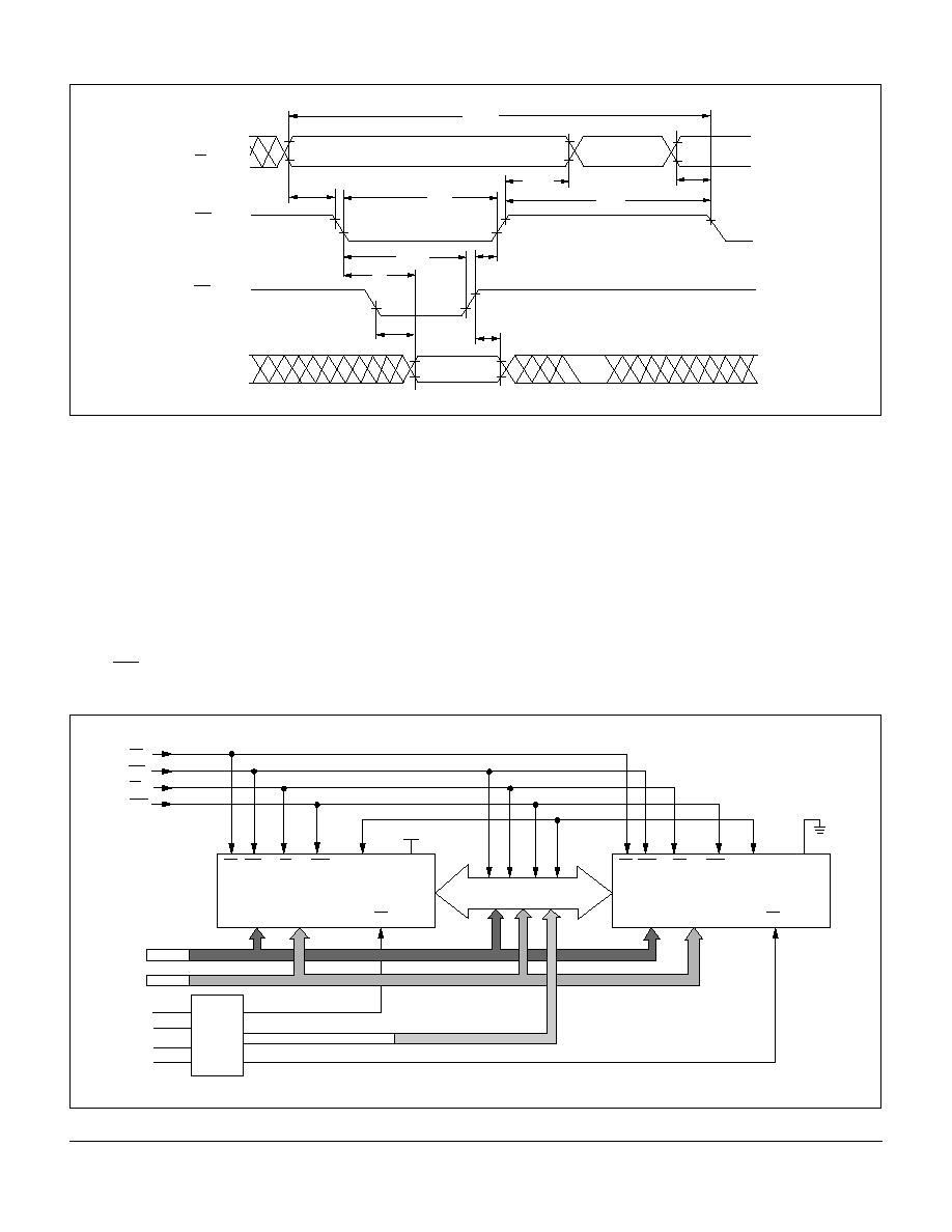
Figure 3. Read Cycle Timing Diagram
Cascading Displays
The HDSP211XS oscillator is designed to drive up to 16 other
HDSP211XSs with input loading of 15 pF each.
The following are the general requirements for cascading 16
displays together:
∑ Determine the correct address for each display.
∑ Use CE from an address decoder to select the correct
display.
∑ Select one of the Displays to provide the clock for the other
displays. Connect CLKSEL to
V
CC
for this display.
∑ Tie CLKSEL to ground on other displays.
∑ Use RTS to synchronize the blinking between the displays.
Figure 4. Cascading Diagram
Tacc
Trd
Tdf
Tr
Tces
Tcer
Tceh
Tacs
Tach
Tacs
A0-A3
FL
Tce
CE
RD
D0-D7
RD WR FL RST CLK I/O CLKSEL
D0-D7 A0-A4 CE
Display
D0-D7 A0-A4 CE
Up to14 More Displays
in between
Address Decode Chip 1 to 14
Address
Data I/O
RD
WR
FL
RST
V
CC
A6
A7
A8
A9
Address
Decoder
RD WR FL RST CLK I/O CLKSEL
0
15
Display
2000 Infineon Technologies Corp. ∑ Optoelectronics Division ∑ San Jose, CA
HDSP2110S/1S/2S/3S/4S/5S
www.infineon.com/opto ∑ 1-888-Infineon (1-888-463-4636)
OSRAM Opto Semiconductors GmbH & Co. OHG ∑ Regensburg, Germany
www.osram-os.com ∑ +49-941-202-7178
4
March 24, 2000-13
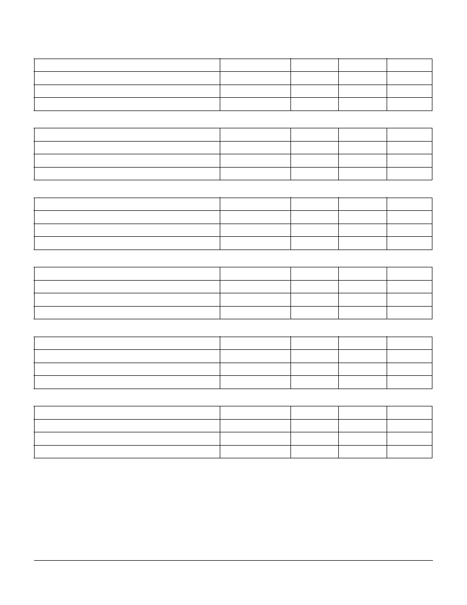
Optical Characteristics at 25
∞
C
(
V
CC
=5.0 V at full brightness)
Red HDSP2110S
Yellow HDSP2111S
High Efficiency Red HDSP2112S
Green HDSP2113S
High Efficiency Green HDSP2114S
Soft Orange HDSP2115S
Note:
1)
Peak luminous intensity is measured at
T
A
=
T
J
=25
∞
C. No time is allowed for the device to warm up prior to measurement.
Description
Symbol
Min.
Typ.
Units
Peak Luminous Intensity
(1)
I
V
peak
70
90
µ
cd/dot
Peak Wavelength
peak
--
660
nm
Dominant Wavelength
dom
--
639
nm
Description
Symbol
Min.
Typ.
Units
Peak Luminous Intensity
(1)
I
V
peak
130
210
µ
cd/dot
Peak Wavelength
peak
--
583
nm
Dominant Wavelength
dom
--
585
nm
Description
Symbol
Min.
Typ.
Units
Peak Luminous Intensity
(1)
I
V
peak
150
330
µ
cd/dot
Peak Wavelength
peak
--
630
nm
Dominant Wavelength
dom
--
620
nm
Description
Symbol
Min.
Typ.
Units
Peak Luminous Intensity
(1)
I
V
peak
150
260
µ
cd/dot
Peak Wavelength
peak
--
565
nm
Dominant Wavelength
dom
--
570
nm
Description
Symbol
Min.
Typ.
Units
Peak Luminous Intensity
(1)
I
V
peak
200
510
µ
cd/dot
Peak Wavelength
peak
--
568
nm
Dominant Wavelength
dom
--
574
nm
Description
Symbol
Min.
Typ.
Units
Peak Luminous Intensity
(1)
I
V
peak
150
270
µ
cd/dot
Peak Wavelength
peak
--
610
nm
Dominant Wavelength
dom
--
604
nm

2000 Infineon Technologies Corp. ∑ Optoelectronics Division ∑ San Jose, CA
HDSP2110S/1S/2S/3S/4S/5S
www.infineon.com/opto ∑ 1-888-Infineon (1-888-463-4636)
OSRAM Opto Semiconductors GmbH & Co. OHG ∑ Regensburg, Germany
www.osram-os.com ∑ +49-941-202-7178
5
March 24, 2000-13
Electrical Characteristics at 25
∞
C
Notes:
1)
I
CC
is an average value.
2)
I
CC
is measured with the display at full brightness. Peak
I
CC
=
28
/
15
I
CC
average (#displayed).
Recommended Operating Conditions
(
T
A
=≠40
∞
C to +85
∞
C)
Parameters
Limits
Conditions
Min.
Typ.
Max.
Units
V
CC
4.5
5.0
5.5
V
--
I
CC
Blank
--
0.65
1.0
mA
V
CC
=5.0 V,
V
IN
=5.0 V
I
CC
12 dots/digit on
(1) (2)
--
185
255
mA
V
CC
=5.0 V, "V" in all 8 digits
I
CC
20 dots/digit on
(1) (2)
--
284
370
mA
V
CC
=5.0 V, "#" in all 8 digits
I
ILP
(with pull-up)
Input Leakage
≠18
≠11
≠5.0
µ
A
V
CC
=5.0 V, V
IN
=0 V to V
CC
,
(WR, CE, FL, RST, RD, CLKSEL)
I
IL
(no pull-up)
Input Leakage
≠1.0
--
+1.0
µ
A
V
CC
=5.0 V, V
IN
=0≠5 V,
(CLK, A0≠A3, D0≠D7)
V
IH
Input Voltage High
2.0
--
V
CC
+0.3
V
V
CC
=4.5 V to 5.5 V
V
IL
Input Voltage Low
GND
≠0.3
--
--
V
V
CC
=4.5 V to 5.5 V
V
OL
(D0≠D7), Output Voltage Low
--
--
0.4
V
V
CC
=4.5 V, I
OL
=1.6 mA
V
OL
(CLK), Output Voltage Low
--
--
0.4
V
V
CC
=4.5 V, I
OL
=40
µ
A
V
OH
Output Voltage High
2.4
--
--
V
V
CC
=4.5 V, I
OH
=≠40
µ
A
JC
Thermal Resistance,
Junction to Case
--
25
--
∞
C/W
--
Clock I/O Frequency
28
57.34
81.14
kHz
V
CC
=4.5 to 5.5 V
FM, Digit Multiplex Frequency
125
256
362.5
Hz
V
CC
=4.5 to 5.5 V
Blinking Rate
0.98
2.0
2.83
Hz
--
Clock I/O Buss Loading
--
--
2.40
pF
--
Clock Out Rise Time
--
--
500
nsec
V
CC
=4.5 V, V
OH
=2.4 V
Clock Out Fall Time
--
--
500
nsec
V
CC
=4.5 V, V
OH
=0.4 V
Parameter
Symbol
Min.
Max.
Units
Supply Voltage
V
CC
4.5
5.5
V
Input Voltage Low
V
IL
--
0.8
V
Input Voltage High
V
IH
2.0
--
V
Output Voltage Low
V
OL
--
0.4
V
Output Voltage High
V
OH
2.4
--
V

2000 Infineon Technologies Corp. ∑ Optoelectronics Division ∑ San Jose, CA
HDSP2110S/1S/2S/3S/4S/5S
www.infineon.com/opto ∑ 1-888-Infineon (1-888-463-4636)
OSRAM Opto Semiconductors GmbH & Co. OHG ∑ Regensburg, Germany
www.osram-os.com ∑ +49-941-202-7178
6
March 24, 2000-13
Figure 5. Top View
Pin Assignment
Pin
Function
Definition
1
RST
Used to initialize a display and
sychronize blinking for multiple
displays
2
FL
Low input accesses the Flash RAM
3
A0
Address input LSB
4
A1
Address input
5
A2
Address input MSB
6
A3
Mode selector
7
V
CC
Optional connection to positive
power supply input.
8
V
CC
9
V
CC
10
A4
Mode Selector
11
CLKSEL
Selects internal/high clock source
28 Pins 15
1 Pins 14
Digit
0 1 2 3 4 5 6 7
Figure 6. Character Set
ASCII
CODE
D0
D1
D2
D3
L
L
L
L
0
H
L
L
L
1
L
H
L
L
2
H
H
L
L
3
L
L
H
L
4
H
L
H
L
5
L
H
H
L
6
H
H
H
L
7
L
L
L
H
8
H
L
L
H
9
L
H
L
H
A
H
H
L
H
B
L
L
H
H
C
H
L
H
H
D
L
H
H
H
E
H
H
H
H
F
L
L
L
L
H
H
H
H
X
L
L
L
L
L
L
L
L
H
L
L
H
H
L
L
H
H
X
L
H
L
H
L
H
L
H
X
0
1
2
3
4
5
6
7
8
D6
D7
D5 D4 HEX
UDC
0
UDC
1
UDC
2
UDC
3
UDC
4
UDC
5
UDC
6
UDC
7
UDC
8
UDC
9
UDC
10
UDC
11
UDC
12
UDC
13
UDC
14
UDC
15
Notes:
1. Upon power up, the device will
initialize in a random state.
2. X=don't care.
Pin Assignment (continued)
Pin
Function
Definition
12
CLK I/O
Outputs master clock or inputs
external clock
13
WR
A low will write data into the display
if CE is low
14
V
CC
Positive power supply input
15
GND supply
Analog Ground for LED drivers
16
GND logic
Digital Ground for internal drivers
17
CE
Enables access to the display
18
RD
A low will read data from the display if
CE is low. If read from display is not
required, then RD can be tied to V
CC
19
D0
Data input LSB
20
D1
Data input
21
No pin
--
22
No pin
--
23
D2
Data input
24
D3
Data input
25
D4
Data input
26
D5
Data input
27
D6
Data input
28
D7
Data input MSB, selects ROM,
page 1 or 2
2000 Infineon Technologies Corp. ∑ Optoelectronics Division ∑ San Jose, CA
HDSP2110S/1S/2S/3S/4S/5S
www.infineon.com/opto ∑ 1-888-Infineon (1-888-463-4636)
OSRAM Opto Semiconductors GmbH & Co. OHG ∑ Regensburg, Germany
www.osram-os.com ∑ +49-941-202-7178
7
March 24, 2000-13
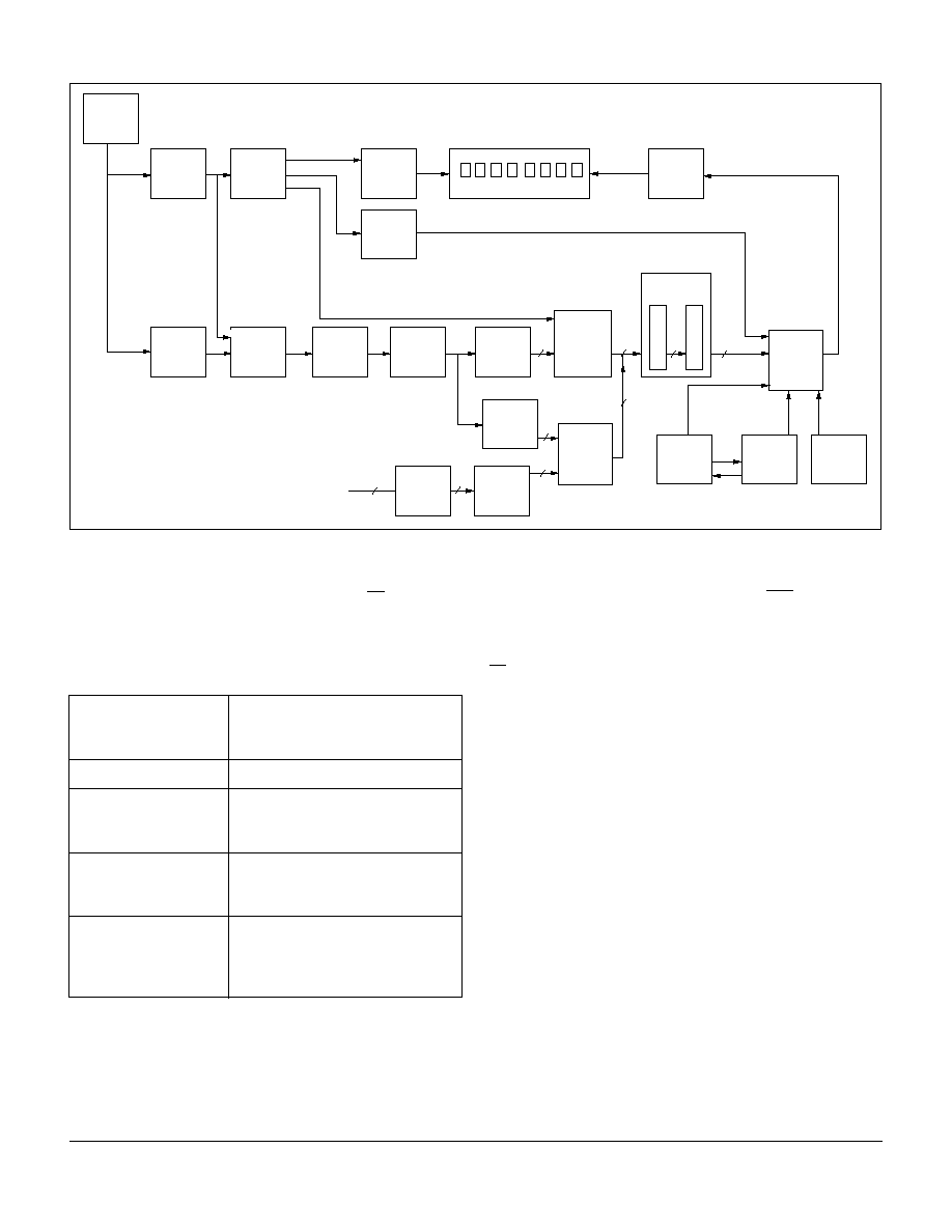
Figure 7. Block Diagram
˜
7
Counter
˜
128
Counter
˜
3
Counter
OSC
Row
Drivers
Column
Drivers
8 Digit Display
Cursor
Controls
and
Display
MUX
D Latch
Holding
Register
ROM
Word
Decode
ROM
Column
Latch
M
a
s
t
e
r
S
l
a
v
e
Character
RAM
Decode
˜
32
Counter
Character
RAM
UDC
Address
Register
Character
Decode
for Display
Character
Decode
(Read/Write)
UDC
RAM
Flash
RAM
Control
Word
Register
Self
Test
Data Bus
25
5
64
16
5
16
4
4
25
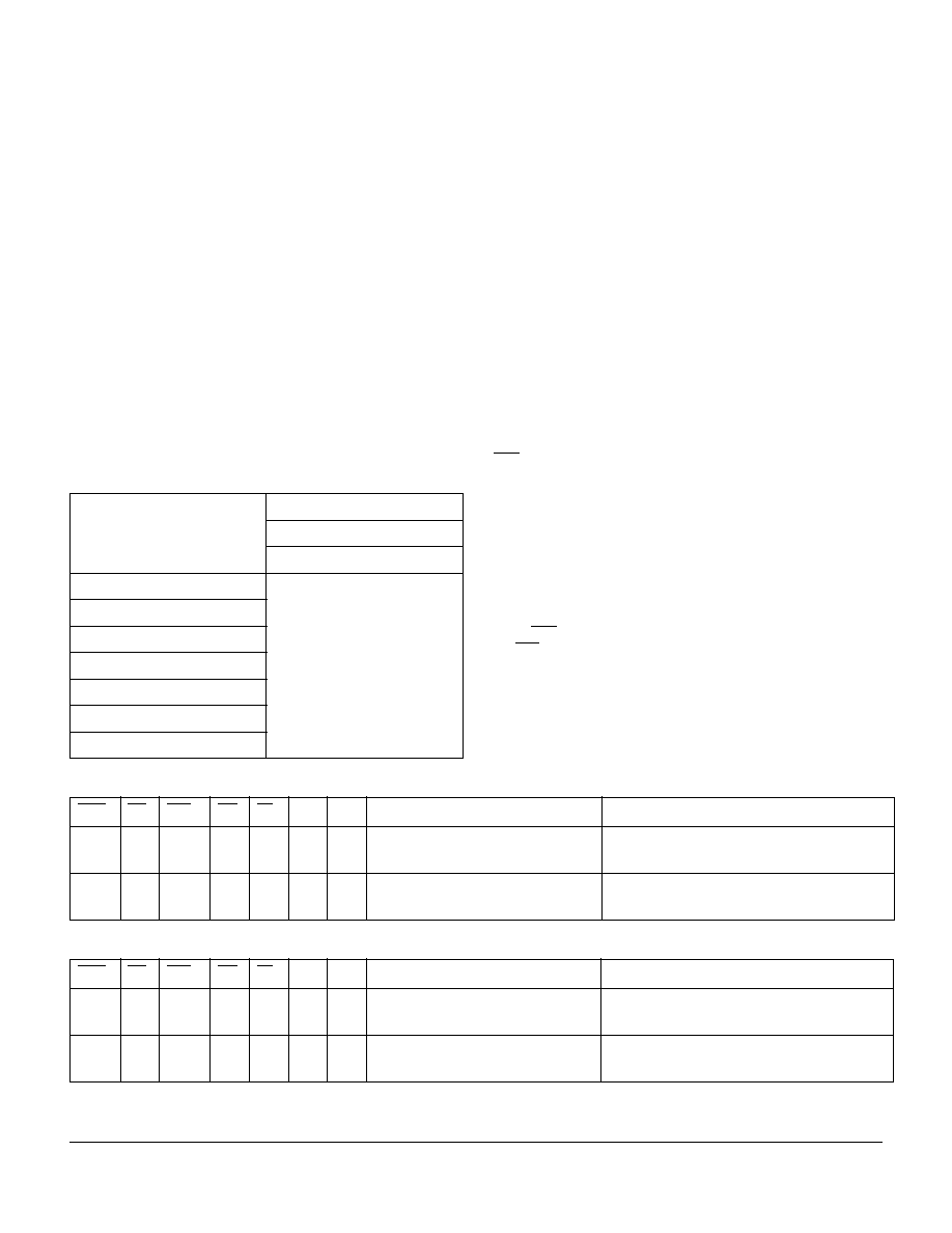
Functional Description
The display's user interface is organized into five memory
areas. They are accessed using the Flash Input, FL, and
address lines, A3 and A4. All the listed RAMs and Registers
may be read or written through the data bus. See Table 1. Each
input pin is described in Pin Definitions.
Five Basic Memory Areas
Character RAM
Stores either ASCII (Katakana)
character data or an UDC RAM
address
Flash RAM
1 x 8 RAM which stores Flash data
User-Defined
Character RAM
(UDC RAM)
Stores dot pattern for custom
characters
User-Defined Address
Register (UDC
Address Register)
Provides address to UDC RAM
when user is writing or reading
custom character
Control Word
Register
Enables adjustment of display
brightness, flash individual charac-
ters, blink, self test or clearing
the display
RST can be used to initialize display operation upon power up
or during normal operation. When activated, RST will clear the
Flash RAM and Control Word Register (00H) and reset the
internal counter. All eight display memory locations will be set
to 20H to show blanks in all digits.
FL pin enables access to the Flash RAM. The Flash RAM will
set (D0=1) or reset (D0=0) flashing of the character addressed
by A0≠A2.
The 1 x 8 bit Control Word Register is loaded with attribute
data if A3=0.
The Control Word Logic decodes attribute data for proper
implementation.
Character ROM is designed for 128 ASCII characters. The
ROM is Mask Programmable for custom fonts.
The Clock Source could either be the internal oscillator
(CLKSEL=1) of the device or an external clock (CLKSEL=0)
could be an input from another HDSP211X display for the syn-
chronization of blinking for multiple displays.
The Display Multiplexer controls the Row Drivers so no addi-
tional logic is required for a display system.
The Display has eight digits. Each digit has 35 LEDs clustered
into a 5 x 7 dot matrix.

2000 Infineon Technologies Corp. ∑ Optoelectronics Division ∑ San Jose, CA
HDSP2110S/1S/2S/3S/4S/5S
www.infineon.com/opto ∑ 1-888-Infineon (1-888-463-4636)
OSRAM Opto Semiconductors GmbH & Co. OHG ∑ Regensburg, Germany
www.osram-os.com ∑ +49-941-202-7178
8
March 24, 2000-13
Table 1. Memory Selection
Theory of operation
The HDSP211XS Programmable Display is designed to work
with all major microprocessors. Data entry is via an eight bit
parallel bus. Three bits of address route the data to the proper
digit location in the RAM. Standard control signals like WR and
CE allow the data to be written into the display.
D0≠D7 data bits are used for both Character RAM and control
word data input. A3 acts as the mode selector.
If A3=1, character RAM is selected. Then input data bit D7 will
determine whether input data bits D0≠D6 is ASCII coded data
(D7=0) or UDC data (D7=1). See section on UDC Address Reg-
ister and RAM.
For normal operation FL pin should be held high. When FL is
held low, Flash RAM is accessed to set character blinking.
The seven bit ASCII code is decoded by the Character ROM to
generate Column data. Twenty columns worth of data is sent
out each display cycle, and it takes fourteen display cycles to
write into eight digits.
The rows are multiplexed in two sets of seven rows each.
The internal timing and control logic synchronizes the turning
on of rows and presentation of column data to assure proper
display operation.
Power Up Sequence
Upon power up display will come on at random. Thus the dis-
play should be reset on power-up. The reset will clear the
Flash RAM, Control Word Register and reset the internal
counter. All the digits will show blanks and display brightness
level will be 100%.
The display must not be accessed until three clock pulses
(110
µ
seconds minimum using the internal clock) after the ris-
ing edge of the reset line.
Microprocessor interface
The interface to a microprocessor is through the 8-bit data
bus (D0≠D7), the 4-bit address bus (A0≠A3) and control lines
FL, CE and WR.
To write data (ASCII/Control Word) into the display CE should
be held low, address and data signals stable and WR should
be brought low. The data is written on the low to high transi-
tion of WR.
The Control Word is decoded by the Control Word Decode
Logic. Each code has a different function. The code for display
brightness changes the duty cycle for the column drivers. The
peak LED current stays the same but the average LED current
diminishes depending on the intensity level.
FL
A4
A3
Section of Memory
A2≠A0
Data Bits Used
0
X
X
Flash RAM
Character Address
D0
1
0
0
UDC Address Register
Don't Care
D3≠D0
1
0
1
UDC RAM
Row Address
D4≠D0
1
1
1
Character RAM
Character Address
D7≠D0
1
1
0
Control Word Register
Don't Care
D7≠D0
The character Flash Enable causes 2.0 Hz coming out of the
counter to be ANDED with column drive signal and makes the
column driver to cycle at 2.0 Hz. Thus the character flashes at
2.0 Hz.
The display Blink works the same way as the Flash Enable but
causes all twenty column drivers to cycle at 2.0 Hz thereby
making all eight digits to blink at 2.0 Hz.
The Self Test function of the IC consists of two internal rou-
tines which exercise major portions of the IC and illuminates
all the LEDs.
Clear bit clears the character RAM and writes a blank into the
display memory. It however does not clear the control word.
ASCII Data or Control Word Data can be written into the display
at this point. For multiple display operation, CLK I/O must be
properly selected. CLK I/O will output the internal clock if
CLKSEL=1, or will allow input from an external clock if
CLKSEL=0.
Character RAM
The Character RAM is selected when FL, A4 and A3 are set to
1,1,1 during a read or write cycle. The Character RAM is a 8 by
8 bit RAM with each of the eight locations corresponding to a
digit on the display. Digit 0 is on the left side of the display and
digit 7 is on the right side of the display. Address lines, A2≠A0
select the digit address with A2 being the most significant bit
and A0 being the least significant bit. The two types of data
stored in the Character RAM are the ASCII coded data and the
UDC Address Data. The type of data stored in the Character
RAM is determined by data bit, D7. If D7 is low, then ASCII
coded data is stored in data bits D6≠D0. If D7 is high, then UDC
Address Data is stored in data bit D3≠D0.
The ASCII coded data is a 7 bit code used to select one of 128
ASCII characters permanently stored in the ASCII ROM.
The UDC Address data is a 4 bit code used to select one of the
UDC characters in the UDC RAM. There are up to 16 charac-
ters available. See Figure 8.
UDC Address Register and UDC RAM
The UDC Address Register and UDC RAM allows the user to
generate and store up to 16 custom characters. Each custom
character is defined in 5 x 7 dot matrix pattern. It takes 8 write
cycles to define a custom character, one cycle to load the UDC
Address Register and 7 cycles to define the character. The con-
tents of the UDC Address Register will store the 4 bit address
for one of the 16 UDC RAM locations. The UDC RAM is used
to store the custom character.

2000 Infineon Technologies Corp. ∑ Optoelectronics Division ∑ San Jose, CA
HDSP2110S/1S/2S/3S/4S/5S
www.infineon.com/opto ∑ 1-888-Infineon (1-888-463-4636)
OSRAM Opto Semiconductors GmbH & Co. OHG ∑ Regensburg, Germany
www.osram-os.com ∑ +49-941-202-7178
9
March 24, 2000-13
Control Word
The Control Word is used to set up the attributes required by
the user. It is addressed by setting FL=1, A4=1, A3=0. The
Control Word is an 8 bit register and is accessed using data
bits, D7≠D0. See Figures 12 and 13 for the logic and attributed
control. The Control Word has 5 functions. They are brightness
control, flashing character enable, blinking character enable,
self test, and clear (Flash and Character RAMS only).
Brightness Control
Control Word bits, D2≠D0, control the brightness of the display
with a binary code of 000 being 100% brightness and 111
being display blank. See Figure 13 for brightness level versus
binary code. The average I
CC
can be calculated by multiplying
the 100% brightness level I
CC
value by the display's brightness
level. For example, a display set to 80% brightness with a
100% average I
CC
value of 200 mA will have an average I
CC
value of 200 mA x 80%=160 mA.
Flash Function
Control Word bit, D3, enables or disables the Flash Function.
When D3 is 1, the Flash Function is enabled and any digit with
its corresponding bit set in the Flash RAM will flash at approxi-
mately 2.0 Hz. When using an external clock, the flash rate can
be determined by dividing the clock rate by 28,672. When D3 is
0, the Flash Function is disabled and the contents of the Flash
RAM is ignored. For synchronized flashing on multiple displays,
see the Reset Section.
UDC Address Register
The UDC Address Register is selected by setting FL=1, A4=0,
A3=0. It is a 4 bit register and uses data bits, D3≠D0 to store
the 4 bit address code (D7≠D4 are ignored). The address code
selects one of 16 UDC RAM locations for custom character
generation.
UDC RAM
The UDC RAM is selected by setting FL=1, A4=0, A3=1. The
RAM is comprised of a 7 x 5 bit RAM. As shown in Figure 11,
address lines, A2≠A0 select one of the 7 rows of the custom
character. Data bits, D4≠D0 determine the 5 bits of column
data in each row. Each data bit corresponds to a LED. If the
data bit is high, then the LED is on. If the data bit is low, the
LED is off. To create a character, each of the 7 rows of column
data need to be defined. See Figures 9 and 10 for logic.
Flash RAM
The Flash RAM allows the display to flash one or more of the
characters being displayed. The Flash Ram is accessed by set-
ting FL low. A4 and A3 are ignored. The Flash RAM is a 8 x 1 bit
RAM with each bit corresponding to a digit address. Digit 0 is
on the left side of the display and digit 7 is on the right side of
the display. Address lines, A2≠A0 select the digit address with
A2 being the most significant digit and A0 being the least sig-
nificant digit. Data bit, D0, sets and resets the flash bit for each
digit. When D0 is high, the flash bit is set and when D0 is low,
It is reset. See Figure 11.
Figure 8. Character RAM Access Logic
Figure 9. UDC Address Register and UDC Character RAM
RST
CE
WR
RD
FL
A4
A3
A2 A1 A0
D7 D6 D5 D4 D3 D2 D1 D0
1
0
0
1
1
1
1
Character Address for
Digits 0≠7
0
7 bit ASCII code for a Write Cycle
1
0
1
0
1
1
1
Character Address for
Digits 0≠7
0
7 bit ASCII code read during a Read Cycle
1
0
0
1
1
0
0
Character Address for
Digits 0≠7
1
D3≠D0=UDC address for a Write Cycle
1
0
1
0
1
0
0
Character Address for
Digits 0≠7
1
D3≠D0=UDC address for Read Data
RST
CE
WR
RD
FL
A4
A3
A2 A1 A0
D7 D6 D5 D4 D3 D2 D1 D0
1
0
0
1
1
0
0
Not used for UDC
Address Register
D3≠D0=UDC RAM Address Code for
Write Cycle
UDC
Address
Register
1
0
1
0
1
0
0
Not used for UDC
Address Register
D3≠D0=UDC RAM Address Code for
Read Cycle
1
0
0
1
1
0
1
A2≠A0=Character
Row Address
D4≠D0=Character Column Data for
Write Cycle
UDC
RAM
1
0
1
0
1
0
1
A2≠A0=Character
Row Address
D4≠D0=Character Column Data read
during a Read Cycle
2000 Infineon Technologies Corp. ∑ Optoelectronics Division ∑ San Jose, CA
HDSP2110S/1S/2S/3S/4S/5S
www.infineon.com/opto ∑ 1-888-Infineon (1-888-463-4636)
OSRAM Opto Semiconductors GmbH & Co. OHG ∑ Regensburg, Germany
www.osram-os.com ∑ +49-941-202-7178
10
March 24, 2000-13
Blink Function
Control Word bit, D4, enables or disables the Blink Function.
When D4 is 1, the Blink Function is enabled and all characters
on the display will blink at approximately 2.0 Hz. The Blink
Function will override the Flash Function if both functions are
enabled. When D4 is 0, the Blink Function is disabled. When
using an external clock, the blink rate can be determined by
dividing the clock rate by 28,672. For synchronized blinking on
multiple displays, see the Reset Section.
Self Test
Before starting Self Test, Reset must first be activated. Control
Word bits, D6 and D5, are used for the Self Test Function.
When D6 is 1, the Self Test is initiated. Results of the Self Test
are stored in bits D5. Control Word bit, D5, is a read only bit.
When D5 is 1, Self Test passed is indicated. When D5 is 0, Self
Test failed is indicated. The Self Test function of the IC consists
of two internal routines which exercise major portions of the IC
and illuminates all of the LEDs. The first routine cycles the
ASCII decoder ROM through all states and performs a check
sum on the output. If the check sum agrees with the correct
value, D5 is set to a 1.
Figure 10. UDC Character Map
Figure 11. Flash RAM Access Logic
Figure 12. Control Word Access Logic
Row Data
A2
A1
A0
Row #
Column Data
C1
C2
C3
C4
C5
D4
D3
D2
D1
D0
0
0
0
1
5 x 7
Dot Matrix
Pattern
0
0
1
2
0
1
0
3
0
1
1
4
1
0
0
5
1
0
1
6
1
1
0
7
RST
CE
WR
RD
FL
A4
A3
A2 A1 A0
D7 D6 D5 D4 D3 D2 D1 D0
1
0
0
1
0
X
X
Flash RAM Address for Digits 0≠7
D0=Flash Data, 0-Flash Off and 1=Flash On
(Write Cycle)
1
0
1
0
0
X
X
Flash RAM Address for Digits 0≠7
D0=Flash Data, 0-Flash Off and 1=Flash On
(Read Cycle)
RST
CE
WR
RD
FL
A4
A3
A2 A1 A0
D7 D6 D5 D4 D3 D2 D1 D0
1
0
0
1
1
1
0
Not used for Control Word
Control Word data for a Write Cycle,
see Figure 13
1
0
1
0
1
1
0
Not used for Control Word
Control Word data for a Read during a
Read Cycle
The second routine provides a visual test of the LEDs using the
drive circuitry. This is accomplished by writing checkered and
inverse checkered patterns to the display. Each pattern is dis-
played for approximately 2.0 seconds. During the self test func-
tion the display must not be accessed. The time needed to
execute the self test function is calculated by multiplying the
clock time by 262,144 (typical time
4.6 sec.). At the end of the
self test function, the Character RAM is loaded with blanks; the
Control Word Register is set to zeroes except D5, and the
Flash RAM is cleared and the UDC Address Register is set to
all 1.0 s.
Clear Function (see Figures 13 and 14)
Control Word bit, D7 clears the character RAM to 20 hex and
the flash RAM to all zeroes. The RAMs are cleared within three
clock cycles (110
µ
s minimum, using the internal clock) when
D7 is set to 1. During the clear time the display must not be
accessed. When the clear function is finished, bit 7 of the
Control Word RAM will be reset to a "0".
Reset Function
The display should be reset on power up of the display
(RST=LOW). When the display is reset, the Character RAM,
Flash RAM, and Control Word Register are cleared.
The display's internal counters are reset. Reset cycle takes
three clock cycles (110
µ
seconds minimum using the internal
clock). The display must not be accessed during this time.
To synchronize the flashing and blinking of multiple displays, it
is necessary for the display to use a common clock source and
reset all the displays at the same time to start the internal
counters at the same place.
While RST is low, the display must not be accessed by RD
nor WR.

2000 Infineon Technologies Corp. ∑ Optoelectronics Division ∑ San Jose, CA
HDSP2110S/1S/2S/3S/4S/5S
www.infineon.com/opto ∑ 1-888-Infineon (1-888-463-4636)
OSRAM Opto Semiconductors GmbH & Co. OHG ∑ Regensburg, Germany
www.osram-os.com ∑ +49-941-202-7178
11
March 24, 2000-13
Figure 13. Control Word Data Definition
Figure 14. Clear Function
X=don't care
Figure 15. Display Cycle Using Built-in ROM Example
Display message "Showtime." Digit 0 is leftmost--closest to pin 1.
Logic levels: 0=Low, 1=High, X=Don't care.
CE
WR
FL
AL
A3
A2
A1
A0
D7
D6
D5
D4
D3
D2
D1
D0
Operation
0
0
0
0
1
1
1
1
0
0
X
X
X
X
X
X
0
1
X
X
X
X
X
X
X
X
X
X
X
X
X
X
Clear disabled
Clear user RAM, page
RAM, flash RAM and dis-
play
RST
CE
WR RD
FL
A4 A3 A2 A1 A0 D7 D6 D5 D4 D3 D2 D1 D0 Operation
Display
0
X
1
1
1
X
X
X
X
X
X
X
X
X
X
X
X
X
Reset. No Read/Write
Within 3 Clock Cycles
All Blank
1
0
0
1
1
1
0
X
X
X
0
0
X
0
0
0
1
1
53% Brightness
Selected
All Blank
1
0
0
1
1
1
1
0
0
0
0
1
0
1
0
0
1
1
Write "S" to Digit 0
S
1
0
0
1
1
1
1
0
0
1
0
1
0
0
1
0
0
0
Write "H" to Digit 1
SH
1
0
0
1
1
1
1
0
1
0
0
1
0
0
1
1
1
1
Write "O" to Digit 2
SHO
1
0
0
1
1
1
1
0
1
1
0
1
0
1
0
1
1
1
Write "W" to Digit 3
SHOW
1
0
0
1
1
1
1
1
0
0
0
1
0
1
0
1
0
0
Write "T" to Digit 4
SHOWT
1
0
0
1
1
1
1
1
0
1
0
1
0
0
1
0
0
1
Write "I" to Digit 5
SHOWTI
1
0
0
1
1
1
1
1
1
0
0
1
0
0
1
1
0
1
Write "M" to Digit 6
SHOWTIM
1
0
0
1
1
1
1
1
1
1
0
1
0
0
0
1
0
1
Write "E" to Digit 7
SHOWTIME
D7 D6 D5 D4 D3 D2 D1 D0
C ST ST BL FL Br Br Br
0 0 0 100% Brightness
0 0 1 80% Brightness
0 1 0 53% Brightness
0 1 1 40% Brightness
1 0 0 27% Brightness
1 0 0 20% Brightness
1 1 0 13% Brightness
1 1 1 Blank Display
0 Flash Function Disabled
1 Flash Function Enabled
0 Blink Function Disabled
1 Blink Function Enabled (overrides Flash Function)
X Normal Operation X=bit ignored
R Run Self Test, R=Test Result, R=1/pass, 0=fail
0
1
0 Normal Operation
1 Clear Flash RAM & Character RAM (Character RAM=20 Hex)
Key
C
Clear Function
ST
Self test
BL
Blink function
FL
Flash function
Br
Brightness control

2000 Infineon Technologies Corp. ∑ Optoelectronics Division ∑ San Jose, CA
HDSP2110S/1S/2S/3S/4S/5S
www.infineon.com/opto ∑ 1-888-Infineon (1-888-463-4636)
OSRAM Opto Semiconductors GmbH & Co. OHG ∑ Regensburg, Germany
www.osram-os.com ∑ +49-941-202-7178
12
March 24, 2000-13
Figure 16. Displaying User Defined Character Example
Load character "A" into UDC-5 and then display it in digit 2
Logic levels: 0=Low, 1=High, X=Don`t care
Electrical and Mechanical Considerations
Voltage Transient Suppression
For best results power the display and the components that
interface with the display to avoid logic inputs higher than V
CC
.
Additionally, the LEDs may cause transients in the power sup-
ply line while they change display states. The common practice
is to place a parallel combination of a .01
µ
F and a 22
µ
F capac-
itor between V
CC
and GND for all display packages.
ESD Protection
The input protection structure of the HDSP211XS provides sig-
nificant protection against ESD damage. It is capable of with-
standing discharges greater than 2.0 kV. Take all the standard
precautions, normal for CMOS components. These include
properly grounding personnel, tools, tables, and transport carri-
ers that come in contact with unshielded parts. If these condi-
tions are not, or cannot be met, keep the leads of the device
shorted together or the parts in antistatic packaging.
Soldering
Considerations
The HDSP211XS can be hand soldered with SN63 solder using
a grounded iron set to 260
∞
C.
Wave soldering is also possible following these conditions:
Preheat that does not exceed 93
∞
C on the solder side of the PC
board or a package surface temperature of 85
∞
C. Water soluble
organic acid flux (except carboxylic acid) or rosin-based RMA
flux without alcohol can be used.
Direct contact with alcohol or alcohol vapor will cause degrada-
tion of the package.
Wave temperature of 245
∞
C
±
5
∞
C with a dwell between 1.5
sec. to 3.0 sec. Exposure to the wave should not exceed
temperatures above 260∞C for five seconds at 0.063" below
the seating plane. The packages should not be immersed in
the wave.
RST CE
WR RD
FL
A4 A3 A2 A1 A0 D7 D6 D5 D4 D3 D2 D1 D0 Operation
Display
0
X
1
1
1
X
X
X
X
X
X
X
X
X
X
X
X
X
Reset. No Read/Write
Within 3 Clock Cycles
All Blank
1
0
0
1
1
0
0
X
X
X
X
X
X
X
0
1
0
1
Select UDC-5
All Blank
1
0
0
1
1
0
1
0
0
0
X
X
X
0
1
1
1
0
Write into Row 1 of UDC-5
All Blank
1
0
0
1
1
0
1
0
0
1
X
X
X
1
0
0
0
1
Write into Row 2 of UDC-5
All Blank
1
0
0
1
1
0
1
0
1
0
X
X
X
1
0
0
0
1
Write into Row 3 of UDC-5
All Blank
1
0
0
1
1
0
1
0
1
1
X
X
X
1
1
1
1
1
Write into Row 4 of UDC-5
All Blank
1
0
0
1
1
0
1
1
0
0
X
X
X
1
0
0
0
1
Write into Row 5 of UDC-5
All Blank
1
0
0
1
1
0
1
1
0
1
X
X
X
1
0
0
0
1
Write into Row 6 of UDC-5
All Blank
1
0
0
1
1
0
1
1
1
0
X
X
X
1
0
0
0
1
Write into Row 7 of UDC-5
All Blank
1
0
0
1
1
1
1
0
1
0
1
X
X
X
0
1
0
1
Write UDC-5 into Digit 2
(Digit 2) A
Post Solder Cleaning Procedures
The least offensive cleaning solution is hot D.I. water (60∞C) for
less than 15 minutes. Addition of mild saponifiers is accept-
able. Do not use commercial dishwasher detergents.
For faster cleaning, solvents may be used. Exercise care in
choosing solvents as some may chemically attack the nylon
package. Maximum exposure should not exceed two minutes
at elevated temperatures. Acceptable solvents are TF (trichorot-
rifluorethane), TA, 111 Trichloroethane, and unheated ace-
tone.
(1)
Note:
1)
Acceptable commercial solvents are: Basic TF, Arklone, P.
Genesolv, D. Genesolv DA, Blaco-Tron TF, Blaco-Tron TA, and
Freon TA.
Unacceptable solvents contain alcohol, methanol, methylene
chloride, ethanol, TP35, TCM, TMC, TMS+, TE, or TES.
Since many commercial mixtures exist, contact a solvent
vendor for chemical composition information. Some major
solvent manufacturers are: Allied Chemical Corporation,
Specialty Chemical Division, Morristown, NJ; Baron-
Blakeslee, Chicago, IL; Dow Chemical, Midland, MI; E.I.
DuPont de Nemours & Co., Wilmington, DE.
For further information refer to Appnotes 18 and 19 at
www.infineon.com/opto.
An alternative to soldering and cleaning the display modules is
to use sockets. Naturally, 28 pin DIP sockets .600" wide with
.100" centers work well for single displays. Multiple display
assemblies are best handled by longer SIP sockets or DIP sock-
ets when available for uniform package alignment. Socket man-
ufacturers are Aries Electronics, Inc., Frenchtown, NJ; Garry
Manufacturing, New Brunswick, NJ; Robinson-Nugent, New
Albany, IN; and Samtec Electronic Hardward, New Albany, IN.
For further information refer to Appnote 22 at www.infin-
eon.com/opto.

2000 Infineon Technologies Corp. ∑ Optoelectronics Division ∑ San Jose, CA
HDSP2110S/1S/2S/3S/4S/5S
www.infineon.com/opto ∑ 1-888-Infineon (1-888-463-4636)
OSRAM Opto Semiconductors GmbH & Co. OHG ∑ Regensburg, Germany
www.osram-os.com ∑ +49-941-202-7178
13
March 24, 2000-13
Optical Considerations
The .200" high character of the HDSP211XS gives readability up
to eight feet. Proper filter selection enhances readability over
this distance.
Using filters emphasizes the contrast ratio between a lit LED
and the character background. This will increase the discrimina-
tion of different characters. The only limitation is cost. Take into
consideration the ambient lighting environment for the best
cost/benefit ratio for filters.
Incandescent (with almost no green) or fluorescent (with
almost no red) lights do not have the flat spectral response of
sunlight. Plastic band-pass filters are an inexpensive and effec-
tive way to strengthen contrast ratios. The HDSP2110/2112S
are red/high efficiency red displays and should be matched
with long wavelength pass filter in the 570 nm to 590 nm
range. The HDSP2113S should be matched with a yellow-
green band-pass filter that peaks at 565 nm. For displays of
multiple colors, neutral density grey filters offer the best com-
promise.
Additional contrast enhancement is gained by shading the dis-
plays. Plastic band-pass filters with built-in louvers offer the
next step up in contrast improvement. Plastic filters can be
improved further with anti-reflective coatings to reduce glare.
The trade-off is fuzzy characters. Mounting the filters close to
the display reduces this effect. Take care not to overheat the
plastic filter by allowing for proper air flow.
Optimal filter enhancements are gained by using circular
polarized, anti-reflective, band-pass filters. The circular polar-
izing further enhances contrast by reducing the light that
travels through the filter and reflects back off the display to
less than 1%.
Several filter manufacturers supply quality filter materials.
Some of them are: Panelgraphic Corporation, W. Caldwell, NJ;
SGL Homalite, Wilmington, DE; 3M Company, Visual Products
Division, St. Paul, MN; Polaroid Corporation, Polarizer Division,
Cambridge, MA; Marks Polarized Corporation, Deer Park, NY,
Hoya Optics, Inc., Fremont, CA.
One last note on mounting filters: recessing displays and bezel
assemblies is an inexpensive way to provide a shading effect in
overhead lighting situations. Several bezel manufacturers are:
R.M.F. Products, Baklava, IL; Nobody Components, Griffith
Plastic Corp., Burningly, CA; Photo Chemical Products of Cali-
fornia, Santa Monica, CA; I.E.E.-Atlas, Van Nuys, CA.