 | –≠–ª–µ–∫—Ç—Ä–æ–Ω–Ω—ã–π –∫–æ–º–ø–æ–Ω–µ–Ω—Ç: SFH3211-4 | –°–∫–∞—á–∞—Ç—å:  PDF PDF  ZIP ZIP |
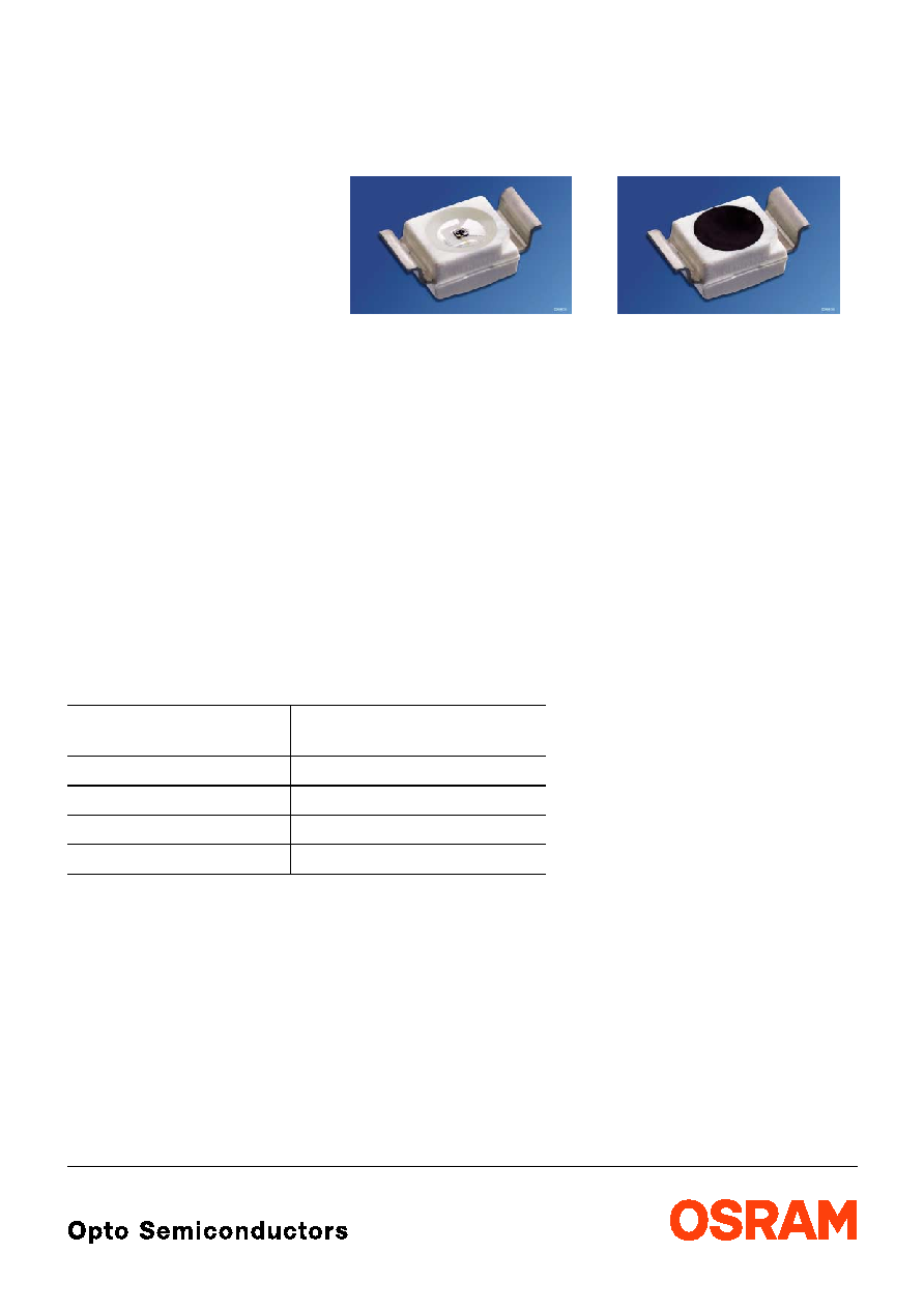
SFH 3211
SFH 3211 FA
NPN-Silizium-Fototransistor in SMT TOPLED
Æ
RG-Geh‰use
Silicon NPN Phototransistor in SMT TOPLED
Æ
RG-Package
SFH 3211
SFH 3211 FA
2002-01-25
1
Wesentliche Merkmale
∑ Speziell geeignet f¸r Anwendungen im Bereich
von 380 nm bis 1150 nm (SFH 3211) und bei
880 nm (SFH 3211 FA)
∑ Hohe Linearit‰t
∑ Gruppiert lieferbar
Anwendungen
∑ Miniaturlichtschranken
∑ Industrieelektronik
∑ ,,Messen/Steuern/Regeln"
Typ
Type
Bestellnummer
Ordering Code
SFH 3211
Q62702-P5127
SFH 3211-3/-4
Q62702-P5481
SFH 3211 FA
Q62702-P5443
SFH 3211 FA-3/-4
Q62702-P5482
Features
∑ Especially suitable for applications from
380 nm to 1150 nm (SFH 3211) and of 880 nm
(SFH 3211 FA)
∑ High linearity
∑ Available in groups
Applications
∑ Miniature photointerrupters
∑ Industrial electronics
∑ For control and drive circuits

2002-01-25
2
SFH 3211, SFH 3211 FA
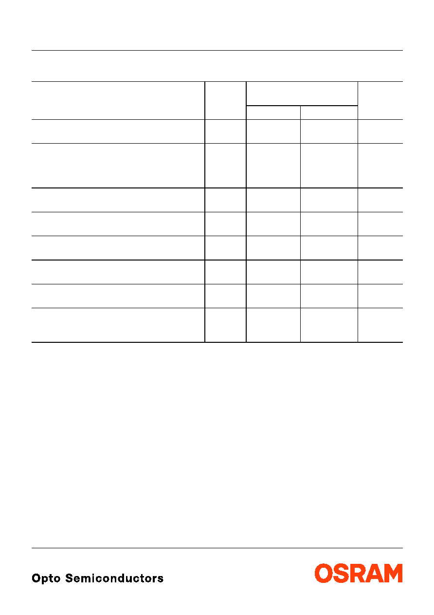
Grenzwerte
Maximum Ratings
Bezeichnung
Parameter
Symbol
Symbol
Wert
Value
Einheit
Unit
Betriebs- und Lagertemperatur
Operating and storage temperature range
T
op
;
T
stg
≠ 40
...
+ 100
∞
C
Kollektor-Emitterspannung
Collector-emitter voltage
V
CE
35
V
Kollektorstrom
Collector current
I
C
15
mA
Kollektorspitzenstrom,
<
10
µ
s
Collector surge current
I
CS
75
mA
Verlustleistung,
T
A
= 25
∞
C
Total power dissipation
P
tot
165
mW
W‰rmewiderstand f¸r Montage auf PC-Board
Thermal resistance for mounting on pcb
R
thJA
450
K/W
SFH 3211, SFH 3211 FA
2002-01-25
3
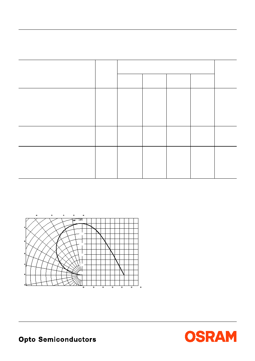
Kennwerte (
T
A
= 25
∞
C,
= 950 nm)
Characteristics
Bezeichnung
Parameter
Symbol
Symbol
Wert
Value
Einheit
Unit
SFH 3211
SFH 3211 FA
Wellenl‰nge der max. Fotoempfindlichkeit
Wavelength of max. sensitivity
S max
860
900
nm
Spektraler Bereich der Fotoempfindlichkeit
S
= 10% von
S
max
Spectral range of sensitivity
S
= 10% of
S
max
380
...
1150
730
...
1120
nm
Bestrahlungsempfindliche Fl‰che (
240
µ
m
)
Radiant sensitive area
A
0.045
0.045
mm
2
Abmessung der Chipfl‰che
Dimensions of chip area
L
◊
B
L
◊
W
0.45
◊
0.45
0.45
◊
0.45
mm
◊
mm
Abstand Chipoberfl‰che zu Geh‰useoberfl‰che
Distance chip front to case surface
H
0.5
...
0.7
0.5
...
0.7
mm
Halbwinkel
Half angle
±
60
±
60
Grad
deg.
Kapazit‰t,
V
CE
= 0 V,
f
= 1 MHz,
E
= 0
Capacitance
C
CE
5.0
5.0
pF
Dunkelstrom
Dark current
V
CE
= 25 V,
E
= 0
I
CEO
1 (
200)
1 (
200)
nA
2002-01-25
4
SFH 3211, SFH 3211 FA
Directional Characteristics
S
rel
=
f
(
)
Die Fototransistoren werden nach ihrer Fotoempfindlichkeit gruppiert und mit arabischen Ziffern
gekennzeichnet.
The phototransistors are grouped according to their spectral sensitivity and distinguished by
arabian figures.
Bezeichnung
Parameter
Symbol
Symbol
Wert
Value
Einheit
Unit
SFH
3211/FA
-2
-3
-4
Fotostrom,
=
950 nm
Photocurrent
E
e
= 0.1 mW/cm
2
,
V
CE
= 5 V
SFH 3211:
E
v
= 1000 Ix, Normlicht/
standard light A,
V
CE
= 5 V
I
PCE
I
PCE
16
16
...
32
420
25
...
50
650
40
...
80
1000
µ
A
µ
A
Anstiegszeit/Abfallzeit
Rise and fall time
I
C
= 1 mA,
V
CC
= 5 V,
R
L
= 1 k
t
r
,
t
f
7
6
7
8
µ
s
Kollektor-Emitter-
S‰ttigungsspannung
Collector-emitter saturation voltage
I
C
=
I
PCEmin
1)
◊
0.3,
E
e
= 0.1 mW/cm
2
V
CEsat
150
150
150
150
mV
1)
I
PCEmin
ist der minimale Fotostrom der jeweiligen Gruppe.
1)
I
PCEmin
is the min. photocurrent of the specified group.
OHF01402
90
80
70
60
50
40
30
20
10
20
40
60
80
100
120
0.4
0.6
0.8
1.0
0.2
0.4
0.6
0.8
1.0
100
0
0
0
SFH 3211, SFH 3211 FA
2002-01-25
5
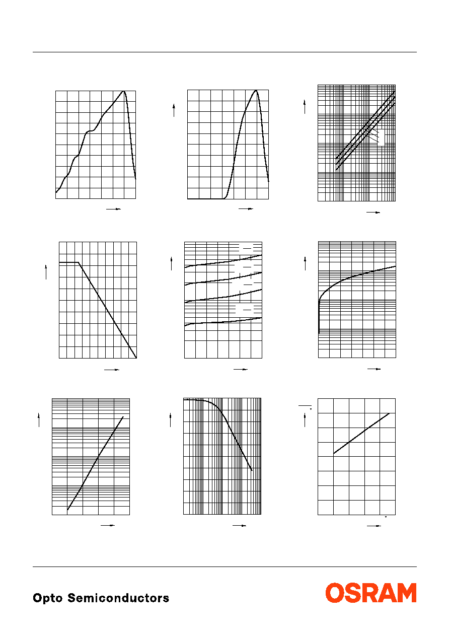
Relative Spectral Sensitivity,
SFH 3211
S
rel
=
f
(
)
Total Power Dissipation
P
tot
=
f
(
T
A
)
Dark Current
I
CEO
=
f
(
T
A
),
V
CE
= 5 V,
E
= 0
0
OHF00207
400
S
rel
nm
%
500 600 700 800 900
1100
10
20
30
40
50
60
70
80
100
OHF00871
tot
P
0
0
40
80
120
160
mW
200
20
40
60
80 ∞C 100
T
A
T
OHF01530
A
CEO
-1
10
10
0
10
1
10
2
10
3
-25
nA
0
25
50
75
100
∞C
Relative Spectral Sensitivity,
SFH 3211 FA
S
rel
=
f
(
)
Photocurrent
I
PCE
=
f
(
V
CE
),
E
e
= Parameter
Capacitance
C
CE
=
f
(
V
CE
),
f
= 1 MHz,
E
= 0
OHF00468
0
rel
S
400
20
40
60
80
%
100
nm
500 600 700 800 900
1100
V
OHF01529
CE
PCE
0
0
10
10
-2
10
-1
mA
V
5
10
15
20
25
30
35
mW
cm
2
0.1
0.25
2
cm
mW
0.5
2
cm
mW
1
2
cm
mW
V
OHF01528
CE
-2
10
CE
C
10
-1
10
0
10
1
10
2
0
V
0.5
1.0
1.5
2.0
2.5
3.0
3.5
4.0
5.0
pF
Photocurrent
I
PCE
=
f
(
E
e
),
V
CE
= 5 V
Dark Current
I
CEO
=
f
(
V
CE
),
E
= 0
Photocurrent
I
PCE
/
I
PCE25∞
=
f
(
T
A
),
V
CE
= 5 V
E
OHF01924
e
PCE
10
-1
10
-3
10
-2
10
0
10
0
10
1
10
2
10
3
2
mW/cm
2
3
4
µ
A
V
OHF01527
CE
CEO
-3
10
10
-2
10
-1
10
0
10
1
0
5
10
15
20
25
30
35
V
nA
T
OHF01524
A
0
-25
0.2
0.4
0.6
0.8
1.0
1.2
1.4
1.6
0
25
50
75
100
PCE
PCE
25
C
2002-01-25
6
SFH 3211, SFH 3211 FA
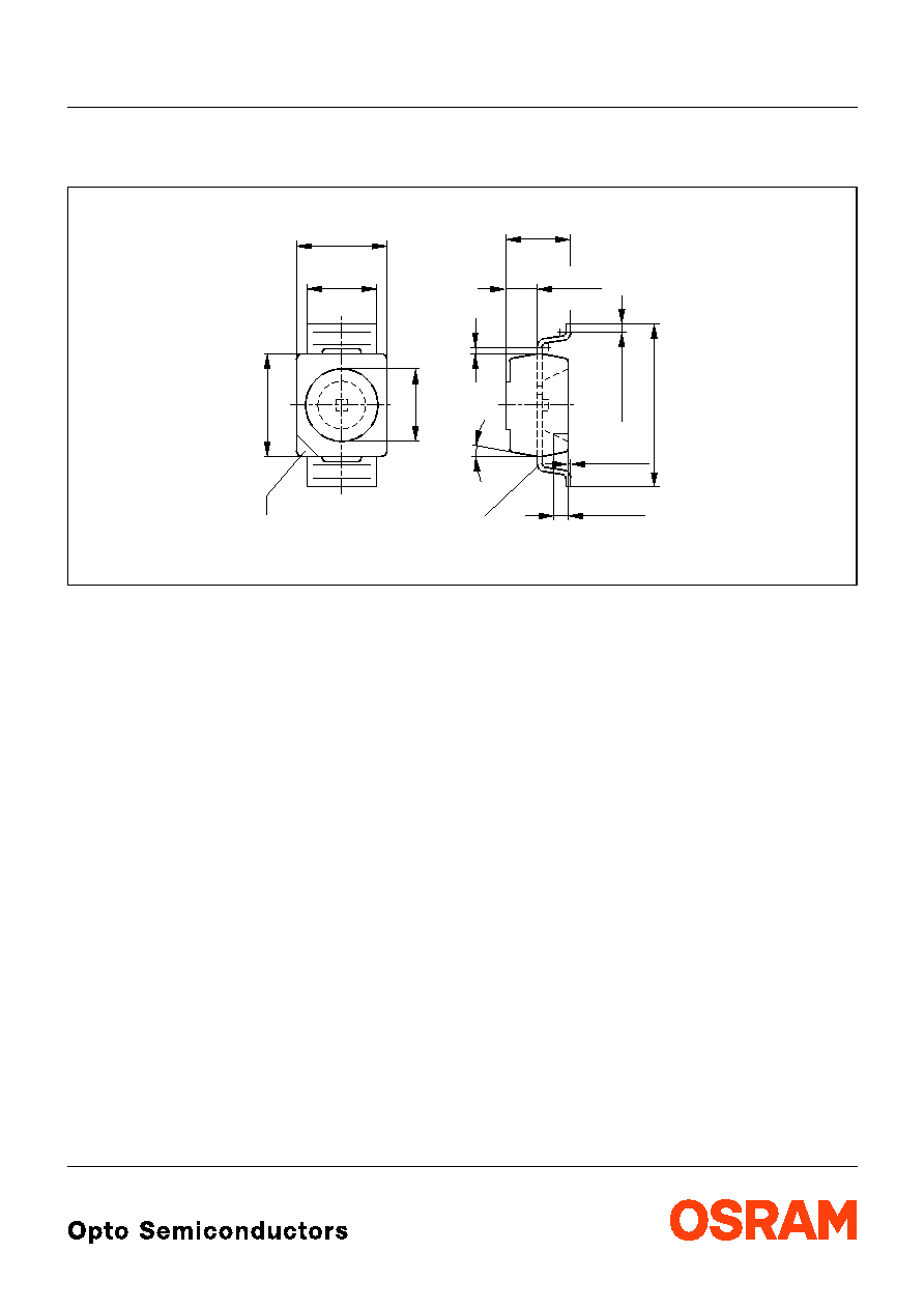
Maþzeichnung
Package Outlines
Maþe werden wie folgt angegeben: mm (inch) / Dimensions are specified as follows: mm (inch).
GPLY6067
0...0.1 (0.004)
Collector marking
4
∞
±1
3.0 (0.118)
2.6 (0.102)
2.3 (0.091)
2.1 (0.083)
3.4 (0.134)
3.0 (0.118)
(2.4 (0.094))
2.1 (0.083)
1.7 (0.067)
5.4 (0.213)
5.0 (0.197)
0.6 (0.024)
0.4 (0.016)
0.3 (0.012) min
0.3 (0.012) max
1.0 (0.039)
0.9 (0.035)
Collector

SFH 3211, SFH 3211 FA
2002-01-25
7
Zus‰tzliche Informationen ¸ber allgemeine Lˆtbedingungen erhalten Sie auf Anfrage.
For additional information on general soldering conditions please contact us.
Published by OSRAM Opto Semiconductors GmbH & Co. OHG
Wernerwerkstrasse 2, D-93049 Regensburg
© All Rights Reserved.
Attention please!
The information describes the type of component and shall not be considered as assured characteristics.
Terms of delivery and rights to change design reserved. Due to technical requirements components may contain
dangerous substances. For information on the types in question please contact our Sales Organization.
Packing
Please use the recycling operators known to you. We can also help you ≠ get in touch with your nearest sales office.
By agreement we will take packing material back, if it is sorted. You must bear the costs of transport. For packing
material that is returned to us unsorted or which we are not obliged to accept, we shall have to invoice you for any costs
incurred.
Components used in life-support devices or systems must be expressly authorized for such purpose! Critical
components
1
, may only be used in life-support devices or systems
2
with the express written approval of OSRAM OS.
1
A critical component is a component usedin a life-support device or system whose failure can reasonably be expected
to cause the failure of that life-support device or system, or to affect its safety or effectiveness of that device or system.
2
Life support devices or systems are intended (a) to be implanted in the human body, or (b) to support and/or maintain
and sustain human life. If they fail, it is reasonable to assume that the health of the user may be endangered.
Lˆthinweise
Soldering Conditions
Bauform
Types
Tauch-, Schwall- und Schlepplˆtung
Dip, Wave and Drag Soldering
Reflowlˆtung
Reflow Soldering
Lˆtbad-
temperatur
Temperature
of the
Soldering
Bath
Maximal
zul‰ssige
Lˆtzeit
Max. Perm.
Soldering
Time
Abstand
Lˆtstelle ≠
Geh‰use
Distance
between
Solder Joint
and Case
Lˆtzonen-
temperatur
Temperature
of Soldering
Zone
Maximale
Durchlaufzeit
Max. Transit
Time
TOPLED RG
260
∞
C
10 s
≠
245
∞
C
10 s