 | –≠–ª–µ–∫—Ç—Ä–æ–Ω–Ω—ã–π –∫–æ–º–ø–æ–Ω–µ–Ω—Ç: OV7411P | –°–∫–∞—á–∞—Ç—å:  PDF PDF  ZIP ZIP |

Version 1.4, March 21, 2003
Proprietary to OmniVision Technologies
1
Advanced Information
Preliminary Datasheet
OV7910 Color CMOS NTSC/PAL C
AMERA
C
HIPTM
OV7411 B&W CMOS NTSC/PAL C
AMERA
C
HIPTM
O
mni
TM
ision
General Description
The OV7910 (color) and OV7411 (black and white) single
chip CMOS C
AMERA
C
HIPSTM
are designed to provide a
high level of functionality in a small footprint package.
Both devices support NTSC/PAL composite video and
S-Video. The OV7910 imager also provides RGB and
YCbCr video signals, and each device directly interfaces
with a VCR TV monitor or other 75 ohm terminated input.
A minimal number of external components are required to
complete a fully functional camera subsystem. The
OV7910/OV7411 video cameras require only a single
5-volt DC supply and have been designed for very low
power operation. These products are ideal for all
applications requiring a small footprint, low voltage, low
power and low cost color or black and white video camera.
Features
∑
Single chip 1/3" format video camera
∑
PAL with 628 x 582 pixels or NTSC with
510 x 492 pixels.
∑
Composite video:
≠
NTSC
≠
S-Video
∑
Component video RGB or YUV
∑
Sensitivity boost (+18 dB)/AGC ON/OFF
∑
Automatic exposure/gain/white balance
∑
External frame sync capability
∑
Aperture correction
∑
SCCB programmable controls:
≠
Color saturation
≠
Brightness
≠
Contrast
≠
White balance
≠
Exposure time
≠
Gain
∑
Gamma correction (0.45) ON/OFF
∑
Low power consumption
∑
+5 volt only power supply
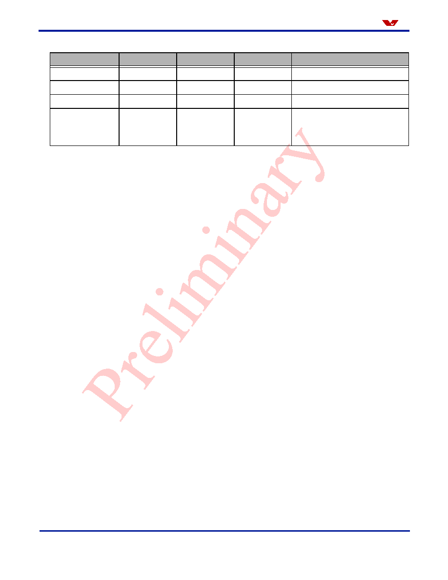
Ordering Information
Product
Package
OV7910 (Color, NTSC/PAL)
CLCC-48
OV7411 (B&W, NTSC/PAL)
CLCC-48
Applications
∑
Automotive
∑
PC Multimedia
∑
Toys
∑
Security
∑
Surveillance
∑
Video phones
∑
Video conference equipment
Key Specifications
Figure 1 OV7910/OV7411 Pin Diagram
Array Size
PAL 628 x 582
NTSC 510 x 492
Power Supply 5 VDC + 5%
Power Requirements 200 mW
Image Area
PAL 5.78 mm x 4.19 mm
NTSC 4.69 mm x 3.54 mm
Auto Electronic Exposure Time 1/60s to 1/2000s
Lens Size 1/3"
Min. Illumination
(3000K)
OV7910 < 5 Lux
OV7411 < 1 Lux
S/N Ratio 40 dB
Pixel Size 9.2 µm x 7.2 µm
Fixed Pattern Noise < 0.03% V
PP
Package Dimensions .560 in. x .560 in.
36
FSI
37
PWDN
38
AMOD0
39
AMOD1
40
HSHP
41
DEVDD
42
DEGND
31
VAXPXO
32
VHSYNC/MIR
33
FSO/VSFR
34
FODD/I2CEN
35
PALSW
13 EVDD
12 SMTAWB
11 RSVD11
10 HSAT
9
CEXP
8
RGSW
7
AVDD
18 OVDD
17 RVCVO
16 GYYO
15 BVCO
14 EGND
48
VR
EF
4
1
SG
N
D
2
SV
D
D
3
Vc
B
R
T
4
BP
AV
E
5
RS
V
D
5
6
AG
ND
43
SC
L
44
SD
A
45
VR
EF
1
46
V
R
EF
2
47
VR
EF
3
OV7910/OV7411
25
DV
DD
24
PA
L
23
XC
L
K
2
22
XC
L
K
1
21
BK
L
T
20
HG
AI
N
19
G2
X
30
AW
B
T
M
29
AW
B
E
N
28
AG
CE
N
27
GA
M
M
A
26
DG
ND

2
Proprietary to OmniVision Technologies
Version 1.4, March 21, 2003
OV7910/OV7411
CMOS NTSC/PAL C
AMERA
C
HIP
TM
O
mni
ision
Functional Description
This section describes the various functions of the OV7910/OV7411. Refer to
Figure 2
for the functional block diagram of the
OV7910/OV7411.
Figure 2 Functional Block Diagram
Clock/Timing Generator and Control Logic
Image Array
(628 X 582)
Row
Select
I
2
C
Interface
Gain
Control
I2
C
E
N
SD
A
SC
L
ASP
Control
CVO
Analog Signal
Processor
(ASP)
XC
L
K
1
XC
L
K
2
PW
D
N
FS
I
BK
L
T
V
c
BRT
G
A
MMA
VH
S
Y
N
C
VA
X
P
X
O
FO
D
D
AMP
Control
Register
Bank
Column Sample/Hold

Functional Description
Version 1.4, March 21, 2003
Proprietary to OmniVision Technologies
3
O
mni
ision
Video Standards
Two TV standards are implemented and available as
output in the OV7910/OV7411 imaging devices,
NTSC (M) and PAL (B).
Table 1
shows how to configure
the standard of choice. Note that the accuracy and
stability of the crystal clock frequency is important to avoid
unwanted color shift in TV video system.
Video Formats
The OV7910/OV7411 image sensors support a variety of
formats including Composite (CVBS), S-Video (YO/CO),
RGB components, and YUV components. Composite and
S-Video signals are generated from the internal TV
encoder and RGB/YUV outputs are generated form the
color matrix prior to entering the encoder. The image
sensor utilizes the RG/BG Bayer pattern, sending raw
pixel data through the color matrix, creating RGB or YUV
component signals. At the same time, YUV signals are
also processed to generate both composite and S-video
signals. Note that color format configuration is valid only
for the OV7910 image sensor.
Composite and S-Video
The Composite/S-Video format is the power-up default
configuration for the OV7910/OV7411 image sensors.
AMOD0
(pin 38) and
AMOD1
(pin 39) select composite
and S-video formats. In this configuration,
RVCVO
(pin 17) outputs the YO component of the S-video signal
and
BVCO
(pin 15) outputs the CO component.
Table 2
summarizes the available formats and the settings
required on the appropriate pins.
RGB Format
Setting AMOD0 = 1 (with AMOD1 = x) selects the RGB
format. In this configuration,
RVCVO
outputs the RED
component,
GYYO
outputs the GREEN component and
BVCO
provides the BLUE component.
Table 1
Standard Configurations
Standard
PAL Setting
(Pin 24)
Clock
Comments
NTSC
0
14.31818 MHz
Clock in =
4 x F
SC
PAL
1
17.734475 MHz
Clock in =
4 x F
SC
YUV Format
Setting
AMOD0
= 0 and
AMOD1
= 1 configures the
OV7910/OV7411 sensors to operate in YUV mode or
B&W mode. In this configuration,
GYYO
outputs the Y
component,
RVCVO
provides the Cr component, and
BVCO
outputs the Cb component. On the OV7411 image
sensor, only the
GYYO
(Y component) output is valid.
Configuring the OV7910/OV7411
The OV7910/OV7411 sensors are designed for
ease-of-use in many standalone applications. Most of the
on-chip functions are configurable by connecting
appropriate pins high (logic "1") or low (logic "0") using a
10K
resistor. The image sensor reads the input pins at
power up which enable user-defined default
configurations.
The OV7910/OV7411 sensors also contain a Serial
Camera Control Bus (SCCB) interface for programmable
access to all register functions. For further details on the
SCCB port, see
"Serial Camera Control Bus (SCCB)" on
page 4
. By default, the SCCB interface is disabled. To
enable the SCCB interface for controlling the sensor, a
10K
. pull-up resistor must be connected to the
FODD/I2CEN
pin (pin 34). With the FODD/I2CEN pin
pulled high at power-up, the OV7910/OV7411 image
sensors will enable the SCCB port for access.
White Balance
The White Balance function in the OV7910/OV7411
image sensor is used to adjust and calibrate the image
device sensitivity on the primary (RGB) colors to match
the color cast of the light source. The Auto White Balance
(AWB) can be enabled or disabled through either the
AWBEN
pin (pin 29) or through the SCCB port. If AWB is
enabled, the image sensors continuously perform white
balancing. A fast or slow mode of white balancing may be
user-selected through the
AWBTM
pin (pin 30). Fast AWB
updates color every 2 fields while slow AWB updates
every 16 fields.
By using the SCCB port, the color temperature may be
further fine tuned to the requirement of the application.
Note that the "blue" (
BLUE
and
BBS
registers) and "red"
(
RED
and
RBS
registers) bias control are only available
through the SCCB port. This function enables the user to
define a "cooler" or "warmer" background for image
capture.
4
Proprietary to OmniVision Technologies
Version 1.4, March 21, 2003
OV7910/OV7411
CMOS NTSC/PAL C
AMERA
C
HIP
TM
O
mni
ision
Table 2
Video Format Options
Format Type
RVCVO (Pin 17)
GYYO (Pin 16)
BUCO (Pin 15)
Pin Settings
Composite/S-Video
CVBS
YO
CO
AMOD0 = 0, AMOD1 = 0
RGB Component
RED
GREEN
BLUE
AMOD0 = 1, AMOD1 = x
YUV Component
Cr
Y
Cb
AMOD0 = 0, AMOD1 = 1
Black and White
--
Y
--
AMOD0 = 0, AMOD1 = 1
Note: Pins 15 and 17 are undefined
in the OV7411 sensor.
Additional Picture Control
A number of functions/registers are available which
enable the user to configure OV7910/OV7411 image
capturing parameters. These functions include Automatic
Gain Control (AGC), AGC Gain, Automatic Exposure
Control (AEC), GAMMA, and Backlight control.
AGC Gain can be set at 2x normal by programming pin 20,
HGAIN
. This function may be configured through the
SCCB port as well.
GAMMA
(pin 27) can be used to set
the color correction.
BKLT
(pin 21) controls how the
OV7910/OV7411 image sensors manage backlight
conditions. These functions may also be controlled by the
SCCB interface.
At power up, AGC and AEC are enabled. AGC can be
disabled at power-up by configuring the
AGCEN
pin
(pin 28) as required. AEC cannot be enabled/disabled
externally and must be programmed through the SCCB
port.
Other Image Sensor Control Functions
Additional programmable functions for OV7910/OV7411
image sensors include sharpness adjustment, brightness
level fine tune, color saturation adjustment, hue
adjustment. All these functions (except for power down)
can be configured by either an external pin or through the
SCCB interface.
Serial Camera Control Bus (SCCB)
Many of the functions and configuration registers in the
OV7910/OV7411 image sensors are available through the
SCCB interface. The SCCB port is enabled by asserting
the I2CEN line (pin 34, see
"FODD/I2CEN" on page 8
)
through a 10K
resistor to V
DD
. When the SCCB
capability is enabled (I2CEN = 1), the OV7910/OV7411
image sensor operates as a slave device that supports up
to 400 kbps serial transfer rate using a 7-bit address/data
transfer protocol.
NOTE: When the SCCB interface is enabled, the
OV7410/OV7411 will output in color by default. To output
in B&W mode, set register
COMB
[1:0] = 10b.
SCCB Protocol Format
In SCCB operation (see
Figure 5
), the master must
perform the following operations:
∑
Generate the Start/Stop condition
∑
Provide the serial clock on SCL
∑
Place the 7-bit slave address (RW bit) and the 8-bit
sub-address on SDA
The receiver must pull down
SDA
during the
acknowledgement bit time. During the write cycle, the
OV7910/OV7411 device returns the acknowledgement
and, during the read cycle, the master returns the
acknowledgement, indicating to the slave that the read
cycle can be terminated. Note that the restart feature is
not supported here.
Within each byte, the MSB is transferred first. The
read/write control bit is the LSB of the first byte. Standard
SCCB communications require only two pins,
SCL
and
SDA
. SDA is configured as an open drain for bidirectional
purposes. A HIGH to LOW transition on the SDA while
SCL is HIGH indicates a START condition. A LOW to
HIGH transition on the SDA while SCL is HIGH indicates
a STOP condition. Only a master can generate
START/STOP conditions.
Except for these two special conditions, the protocol that
SDA remain stable during the HIGH period of the clock,
SCL. Each bit is allowed to change state only when SCL
is LOW (see
Figure 3
and
Figure 4
).
The OV7910/OV7411 SCCB interface supports multi-byte
write and multi-byte read. The master must supply the
sub-address in the write cycle, but not in the read cycle.
Therefore, the OV7910/OV7411 takes the read
sub-address from the previous write cycle. In multi-byte
write or multi-byte read cycles, the sub-address
automatically increments after the first data byte so that
Functional Description
Version 1.4, March 21, 2003
Proprietary to OmniVision Technologies
5
O
mni
ision
continuous locations can be accessed in one bus cycle. A
multi-byte cycle overwrites its original sub-address;
therefore, if a read cycle immediately follows a multi-byte
cycle, a single byte write cycle that provides a new
address must be inserted.
The OV7910/OV7411 supports a single slave ID. The ID
is preset to 80 for write and 81 for read.
In the write cycle, the second byte in the SCCB is the
sub-address for selecting the individual on-chip registers,
and the third byte is the data associated with this register.
Writing to the unimplemented sub-address is ignored.
In the read cycle, the second byte is the data associated
with the previously stored sub-address. Reading of an
unimplemented sub-address returns unknown.
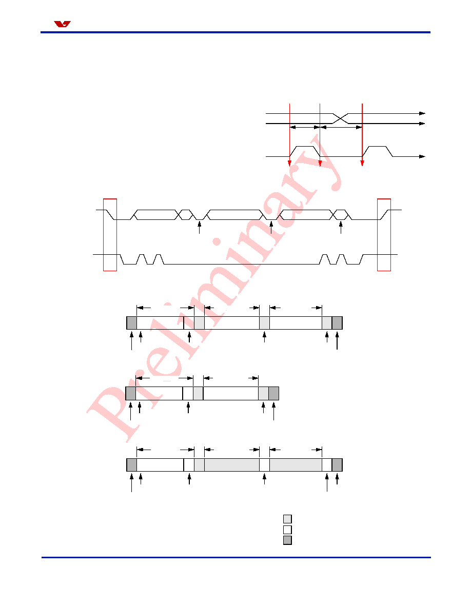
Figure 3 Bit Transfer on the SCCB
DATA
DATA
SDA
SCL
STABLE
CHANGE
ALLOWED
Figure 4 Data Transfer on the SCCB
Figure 5 SCCB Protocol Format
SDA
SCL
SLAVE ID
SUB-ADDRESS
DATA
RW
S
P
A
A
A
RW
SUB-ADDRESS (8-BIT)
DATA (8-BIT)
SLAVE (7-BIT)
S
A
A
A
P
STOP
ACK
ACK
LSB=0
MSB
START
FIRST BYTE
SECOND BYTE
THIRD BYTE
MASTER TRANSMIT, SLAVE RECEIVE (WRITE CYCLE)
RW
SUB-ADDRESS (8-BIT)
SLAVE (7-BIT)
S
A
A
P
STOP
ACK
LSB=0
MSB
START
FIRST BYTE
SECOND BYTE
MASTER TRANSMIT, SLAVE RECEIVE (DUMMY WRITE CYCLE)
RW
DATA (8-BIT)
DATA (8-BIT)
SLAVE (7-BIT)
S
A
A
1
P
STOP
NO ACK IN
ACK
LSB=1
MSB
START
FIRST BYTE
SECOND BYTE
THIRD BYTE
MASTER RECEIVE, SLAVE RECEIVE (READ CYCLE)
LAST BYTE
≠
SLAVE TRANSMIT
≠
MASTER TRANSMIT
≠
MASTER INITIATE
S ≠ START CONDITION
A ≠ ACKNOWLEDGE BIT
P ≠ STOP CONDITION
SLAVE ID ≠ 1000000X
X ≠ RW BIT, 1: READ, 0: WRITE