1
Transistor
2SA1806
Silicon PNP epitaxial planer type
For high speed switching
s
Features
q
High-speed switching.
q
Low collector to emitter saturation voltage V
CE(sat)
.
q
SS-Mini type package, allowing downsizing of the equipment
and automatic insertion through the tape packing and the maga-
zine packing.
s
Absolute Maximum Ratings
(Ta=25∞C)
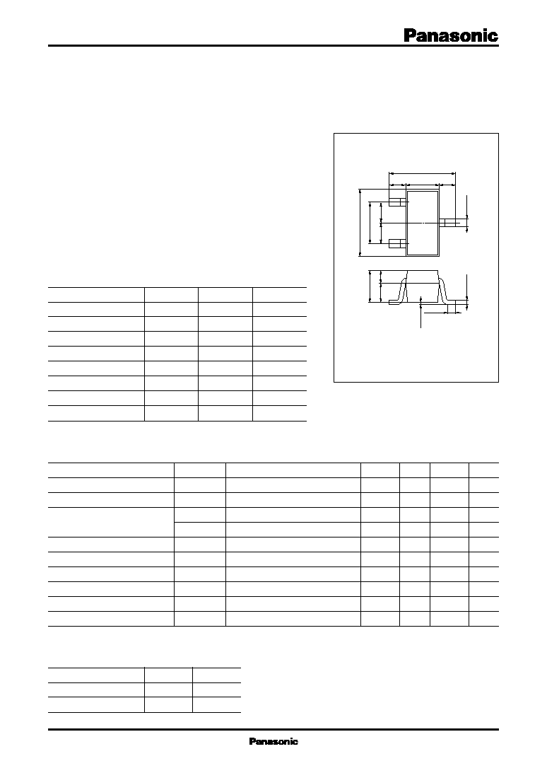
Unit: mm
Parameter
Collector to base voltage
Collector to emitter voltage
Emitter to base voltage
Peak collector current
Collector current
Collector power dissipation
Junction temperature
Storage temperature
1:Base
2:Emitter
EIAJ:SC≠75
3:Collector
SS≠Mini Type Package
Symbol
V
CBO
V
CEO
V
EBO
I
CP
I
C
P
C
T
j
T
stg
Ratings
≠15
≠15
≠4
≠100
≠50
125
125
≠55 ~ +125
Unit
V
V
V
mA
mA
mW
∞C
∞C
s
Electrical Characteristics
(Ta=25∞C)
Parameter
Collector cutoff current
Emitter cutoff current
Forward current transfer ratio
Collector to emitter saturation voltage
Transition frequency
Collector output capacitance
Turn-on time
Turn-off time
Storage time
Symbol
I
CBO
I
EBO
h
FE1
*
h
FE2
V
CE(sat)
f
T
C
ob
t
on
t
off
t
stg
Conditions
V
CB
= ≠8V, I
E
= 0
V
EB
= ≠3V, I
C
= 0
V
CE
= ≠1V, I
C
= ≠10mA
V
CE
= ≠1V, I
C
= ≠1mA
I
C
= ≠10mA, I
B
= ≠ 1mA
V
CB
= ≠10V, I
E
= 10mA, f = 200MHz
V
CB
= ≠5V, I
E
= 0, f = 1MHz
(Note 1) Next page
(Note 1) Next page
(Note 1) Next page
min
50
30
800
typ
≠ 0.1
1500
1
12
20
19
max
≠ 0.1
≠ 0.1
150
≠ 0.2
Unit
µ
A
µ
A
V
MHz
pF
ns
ns
ns
*
h
FE1
Rank classification
Rank
Q
R
h
FE1
50 ~ 120
90 ~ 150
Marking Symbol
AKQ
AKR
1.6
±
0.15
1.6
±
0.1
1.0
±
0.1
0.75
±
0.15
0.45
±
0.1
0.5
0.3
0 to 0.1
0.5
0.8
±
0.1
0.4
0.4
0.2
+0.1 ≠0.05
0.15
+0.1 ≠0.05
1
2
3
0.2
±
0.1
Marking symbol :
AK
2
Transistor
2SA1806
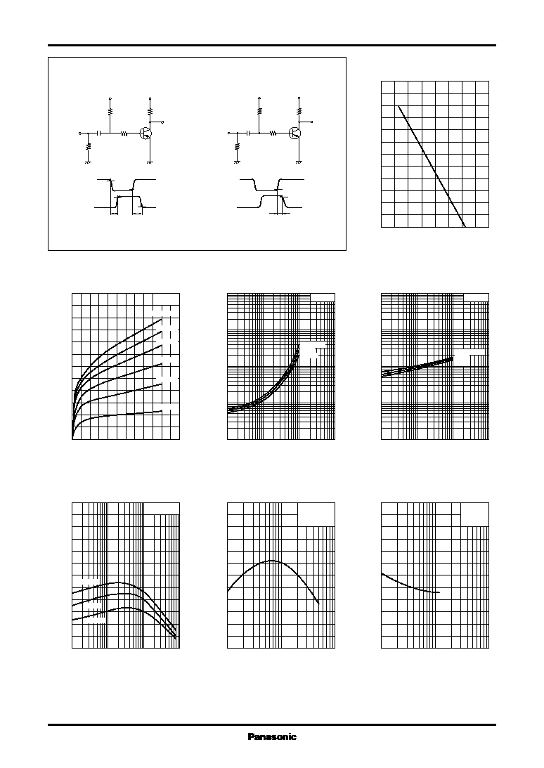
0
160
40
120
80
140
20
100
60
0
150
125
100
75
50
25
Ambient temperature Ta (∞C)
Collector power dissipation P
C
(mW
)
0
≠12
≠10
≠8
≠2
≠6
≠4
0
≠60
≠50
≠40
≠30
≠20
≠10
Ta=25∞C
≠300
µ
A
≠500
µ
A
≠400
µ
A
≠100
µ
A
≠200
µ
A
I
B
=≠600
µ
A
Collector to emitter voltage V
CE
(V)
Collector current I
C
(mA
)
≠1
≠10
≠100
≠1000
≠3
≠30
≠300
≠ 0.01
≠ 0.03
≠ 0.1
≠ 0.3
≠1
≠3
≠10
≠30
≠100
I
C
/I
B
=10
Ta=75∞C
25∞C
≠25∞C
Collector current I
C
(mA)
Collector to emitter saturation voltage V
CE(sat)
(V
)
≠1
≠10
≠100
≠1000
≠3
≠30
≠300
≠ 0.01
≠ 0.03
≠ 0.1
≠ 0.3
≠1
≠3
≠10
≠30
≠100
I
C
/I
B
=10
Ta=≠25∞C
25∞C
75∞C
Collector current I
C
(mA)
Base to emitter saturation voltage V
BE(sat)
(V
)
≠ 0.1
≠1
≠10
≠100
≠ 0.3
≠3
≠30
0
240
200
160
120
80
40
V
CE
=≠10V
Ta=75∞C
25∞C
≠25∞C
Collector current I
C
(mA)
Forward current transfer ratio h
FE
1
3
10
30
100
0
2400
2000
1600
1200
800
400
V
CB
=≠10V
f=200MHz
Ta=25∞C
Emitter current I
E
(mA)
Transition frequency f
T
(MHz
)
≠1
≠3
≠10
≠30
≠100
0
2.4
2.0
1.6
1.2
0.8
0.4
I
E
=0
f=1MHz
Ta=25∞C
Collector to base voltage V
CB
(V)
Collector output capacitance C
ob
(pF
)
2k
62
51
V
BB
V
in
V
in
V
CC
=≠1.5V
V
in
=≠5.8V
V
BB
=Ground
V
in
=9.8V
V
BB
=≠8.0V
V
out
0.1
µ
F
0
52
10%
10%
90%
V
out
90%
t
on
t
off
508
30
51
V
BB
=≠10V
V
in
V
CC
=≠3V
V
in
=9.0V
V
out
0.1
µ
F
34
V
in
0
V
out
90%
t
off
90%
P
C
-- Ta
I
C
-- V
CE
V
CE(sat)
-- I
C
V
BE(sat)
-- I
C
h
FE
-- I
C
f
T
-- I
E
C
ob
-- V
CB
Switching time measurement circuit
t
on
, t
off
Test Circuit
t
stg
Test Circuit