Transistors
1
2SB1434
Silicon PNP epitaxial planer type
For low-frequency output amplification
Complementary to 2SD2177
I Features
∑ Low collector to emitter saturation voltage V
CE(sat)
∑ Allowing supply with the radial taping
I Absolute Maximum Ratings T
a
= 25∞C
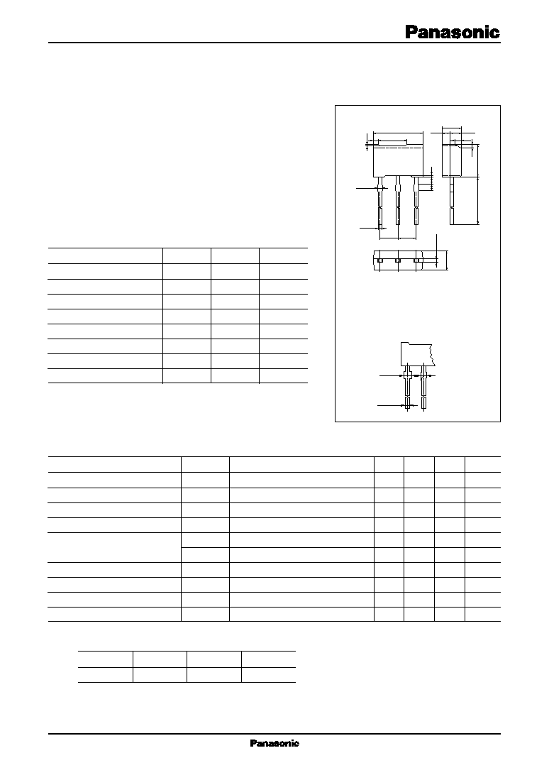
Unit: mm
2.5
±0.1
4.5
±
0.1
14.5
±
0.5
2.5
±0.5 2.5±0.5
2.5
±
0.1
6.9
±0.1
1.05
±0.05
(1.45)
4.0
0.7
0.8
0.15
0.5
0.2
1.0
1.0
0.65 max.
0.45
+0.1
-0.05
0.45
+
0.1
-
0.05
3
2
1
1.2
±0.1
0.65
max.
0.45
0.1
0.05
+
-
(HW Type)
Note) In addition to the
lead type shown in
the upper figure,
the type as shown
in the lower figure
is also available.
1: Emitter
2: Collector
3: Base
MT2 Type Package
Parameter
Symbol
Rating
Unit
Collector to base voltage
V
CBO
-50
V
Collector to emitter voltage
V
CEO
-50
V
Emitter to base voltage
V
EBO
-5
V
Peak collector current
I
CP
-3
A
Collector current
I
C
-2
A
Collector power dissipation
*
P
C
1
W
Junction temperature
T
j
150
∞C
Storage temperature
T
stg
-55 to +150
∞C
Parameter
Symbol
Conditions
Min
Typ
Max
Unit
Collector cutoff current
I
CBO
V
CB
= -20 V, I
E
= 0
- 0.1
µA
Collector to base voltage
V
CBO
I
C
= -10 µA, I
E
= 0
-50
V
Collector to emitter voltage
V
CEO
I
C
= -1 mA, I
B
= 0
-50
V
Emitter to base voltage
V
EBO
I
E
= -10 µA, I
C
= 0
-5
V
Forward current transfer ratio
*1
h
FE1
*2
V
CE
= -2 V, I
C
= -200 mA
120
340
h
FE2
V
CE
= -2 V, I
C
= -1 A
60
Collector to emitter saturation voltage
*1
V
CE(sat)
I
C
= -1 A, I
B
= -50 mA
- 0.2
- 0.3
V
Base to emitter saturation voltage
*1
V
BE(sat)
I
C
= -1 A, I
B
= -50 mA
- 0.85
-1.2
V
Transition frequency
f
T
V
CB
= -10 V, I
E
= 50 mA, f = 200 MHz
110
MHz
Collector output capacitance
C
ob
V
CB
= -10 V, I
E
= 0, f = 1 MHz
40
60
pF
I Electrical Characteristics T
a
= 25∞C ± 3∞C
Rank
R
S
No-rank
h
FE1
120 to 240
170 to 340
120 to 340
Note) *1: Pulse measurement
*2: Rank classification
Product of no-rank is not classified and have no indication for rank.
Note) *: Printed circuit board: Copper foil area of 1 cm
2
or more, and the
board thickness of 1.7 mm for the collector portion
2SB1434
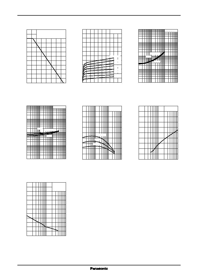
Transistors
2
P
C
T
a
I
C
V
CE
V
CE(sat)
I
C
V
BE(sat)
I
C
h
FE
I
C
f
T
I
E
C
ob
V
CB
0
160
40
120
80
140
20
100
60
0
1.2
1.0
0.8
0.6
0.4
0.2
Copper plate at the collector
is more than 1 cm
2
in area,
1.7 mm in thickness.
Ambient temperature T
a
(
∞C)
Collector power dissipation P
C
(W
)
0
0
≠10
≠2
≠4
≠8
≠6
-2.4
-2.0
-1.6
-1.2
- 0.8
- 0.4
Collector to emitter voltage V
CE
(V)
Collector current I
C
(A
)
T
a
= 25∞C
I
B
= -8 mA
-1 mA
-2 mA
-3 mA
-4 mA
-5 mA
-6 mA
-7 mA
- 0.001
- 0.003
-1
-3
-10
-1
-3
-10
T
a
= 100∞C
25
∞C
-25∞C
Collector to emitter saturation voltage
V
CE(sat)
(V
)
Collector current I
C
(A)
I
C
/ I
B
= 20
- 0.01
- 0.03
- 0.01 - 0.03
- 0.1
- 0.3
- 0.1 - 0.3
-1
-3
-10
-30
-100
-1
-3
-10
T
a
= -25∞C
25
∞C
75
∞C
- 0.01 - 0.03 - 0.1 - 0.3
Base to emitter saturation voltage
V
BE(sat)
(V
)
Collector current I
C
(A)
I
C
/ I
B
= 20
- 0.01
- 0.03
- 0.1
- 0.3
-1
-10
-3
0
100
200
300
500
400
V
CE
= -2 V
T
a
= 100∞C
25
∞C
-25∞C
Forward current transfer ratio h
FE
- 0.01 - 0.03 - 0.1 - 0.3
Collector current I
C
(A)
1
3
10
30
100
0
40
80
120
200
160
Transition frequency f
T
(MHz
)
Emitter current I
E
(mA)
V
CB
= -10 V
T
a
= 25∞C
0
-1
240
200
160
120
80
40
-3
-10
-30
-100
Collector output capacitance C
ob
(
pF
)
Collector to base voltage V
CB
(V)
I
E
= 0
f
= 1 MHz
T
a
= 25∞C