1
Transistor
2SB1539
Silicon PNP epitaxial planer type
For low-frequency amplification
Complementary to 2SD2359
s
Features
q
Low collector to emitter saturation voltage V
CE(sat)
.
q
Large collector power dissipation P
C
.
q
Mini Power type package, allowing downsizing of the equipment
and automatic insertion through the tape packing and the maga-
zine packing.
s
Absolute Maximum Ratings
(Ta=25∞C)
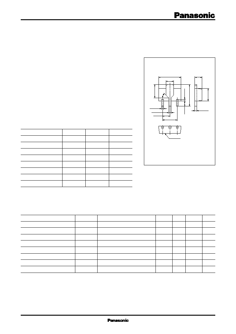
Unit: mm
Parameter
Collector to base voltage
Collector to emitter voltage
Emitter to base voltage
Peak collector current
Collector current
Collector power dissipation
Junction temperature
Storage temperature
1:Base
2:Collector
EIAJ:SC≠62
3:Emitter
Mini Power Type Package
4.5
±
0.1
2.6
±
0.1
2.5
±
0.1
0.4max.
1.0
+0.1
≠0.2
4.0
+0.25
≠0.20
3.0
±
0.15
1.5
±
0.1
0.4
±
0.08
0.5
±
0.08
1.5
±
0.1
0.4
±
0.04
1.6
±
0.2
45
∞
marking
3
2
1
Symbol
V
CBO
V
CEO
V
EBO
I
CP
I
C
P
C
*
T
j
T
stg
Ratings
≠20
≠20
≠5
≠1.2
≠1
1
150
≠55 ~ +150
Unit
V
V
V
A
A
W
∞C
∞C
s
Electrical Characteristics
(Ta=25∞C)
Parameter
Collector cutoff current
Collector to base voltage
Collector to emitter voltage
Emitter to base voltage
Forward current transfer ratio
Collector to emitter saturation voltage
Transition frequency
Collector output capacitance
Symbol
I
CBO
V
CBO
V
CEO
V
EBO
h
FE
V
CE(sat)
f
T
C
ob
Conditions
V
CB
= ≠14V, I
E
= 0
I
C
= ≠10
µ
A, I
E
= 0
I
C
= ≠1mA, I
B
= 0
I
E
= ≠10
µ
A, I
C
= 0
V
CE
= ≠2V, I
C
= ≠100mA
**
I
C
= ≠500mA, I
B
= ≠10mA
**
V
CB
= ≠10V, I
E
= 50mA, f = 200MHz
V
CB
= ≠10V, I
E
= 0, f = 1MHz
min
≠20
≠20
≠5
200
typ
120
30
max
≠1
800
≠ 0.2
Unit
µ
A
V
V
V
V
MHz
pF
*
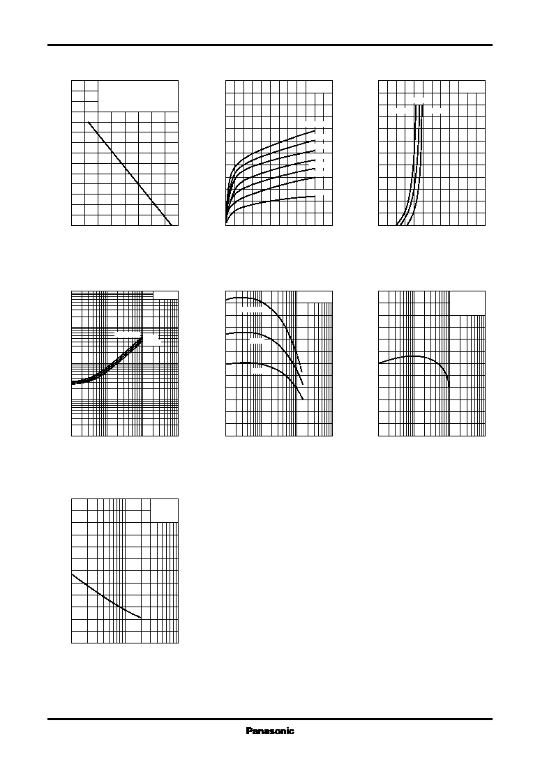
Printed circuit board: Copper foil area of 1cm
2
or more, and the board
thickness of 1.7mm for the collector portion
**
Pulse measurement
Marking symbol :
1N
2
Transistor
2SB1539
0
160
40
120
80
140
20
100
60
0
1.4
1.2
0.4
1.0
0.8
0.2
0.6
Printed circut board: Copper
foil area of 1cm
2
or more, and
the board thickness of 1.7mm
for the collector portion.
Ambient temperature Ta (∞C)
Collector power dissipation P
C
(W
)
0
≠12
≠10
≠8
≠2
≠6
≠4
0
≠1.2
≠1.0
≠ 0.8
≠ 0.6
≠ 0.4
≠ 0.2
Ta=25∞C
≠1.4mA
≠1.2mA
≠1.0mA
≠ 0.8mA
≠ 0.6mA
≠ 0.4mA
I
B
=≠1.6mA
Collector to emitter voltage V
CE
(V)
Collector current I
C
(A
)
0
≠2.4
≠2.0
≠1.6
≠ 0.4
≠1.2
≠ 0.8
0
≠1.2
≠1.0
≠ 0.8
≠ 0.6
≠ 0.4
≠ 0.2
V
CE
=≠2V
Ta=75∞C
≠25∞C
25∞C
Base to emitter voltage V
BE
(V)
Collector current I
C
(A
)
≠ 0.01
≠ 0.1
≠1
≠10
≠ 0.03
≠ 0.3
≠3
≠ 0.001
≠ 0.003
≠ 0.01
≠ 0.03
≠ 0.1
≠ 0.3
≠1
≠3
≠10
I
C
/I
B
=50
Ta=75∞C
25∞C
≠25∞C
Collector current I
C
(A)
Collector to emitter saturation voltage V
CE(sat)
(V
)
≠ 0.01
≠ 0.1
≠1
≠10
≠ 0.03
≠ 0.3
≠3
0
600
500
400
300
200
100
V
CE
=≠2V
Ta=75∞C
25∞C
≠25∞C
Collector current I
C
(A)
Forward current transfer ratio h
FE
1
10
100
1000
3
30
300
0
240
200
160
120
80
40
V
CB
=≠10V
f=200MHz
Ta=25∞C
Emitter current I
E
(mA)
Transition frequency f
T
(MHz
)
≠1
≠3
≠10
≠30
≠100
0
120
100
80
60
40
20
I
E
=0
f=1MHz
Ta=25∞C
Collector to base voltage V
CB
(V)
Collector output capacitance C
ob
(pF
)
P
C
-- Ta
I
C
-- V
CE
I
C
-- V
BE
V
CE(sat)
-- I
C
h
FE
-- I
C
f
T
-- I
E
C
ob
-- V
CB