1
Transistor
2SC5473 (Tentative)
Silicon NPN epitaxial planer type
For low-voltage low-noise high-frequency oscillation
s
Features
q
High transition frequency f
T
.
q
High gain of 8.9dB and low noise of 1.8dB at 3V.
q
Optimum for RF amplification of a portable telephone and
pager.
q
S-Mini type package, allowing downsizing of the equipment and
automatic insertion through the tape packing and the magazine
packing.
s
Absolute Maximum Ratings
(Ta=25∞C)
Parameter
Collector to base voltage
Collector to emitter voltage
Emitter to base voltage
Collector current
Collector power dissipation
Junction temperature
Storage temperature
Symbol
V
CBO
V
CEO
V
EBO
I
C
P
C
T
j
T
stg
Ratings
9
6
1
30
150
150
≠55 ~ +150
Unit
V
V
V
mA
mW
∞C
∞C
s
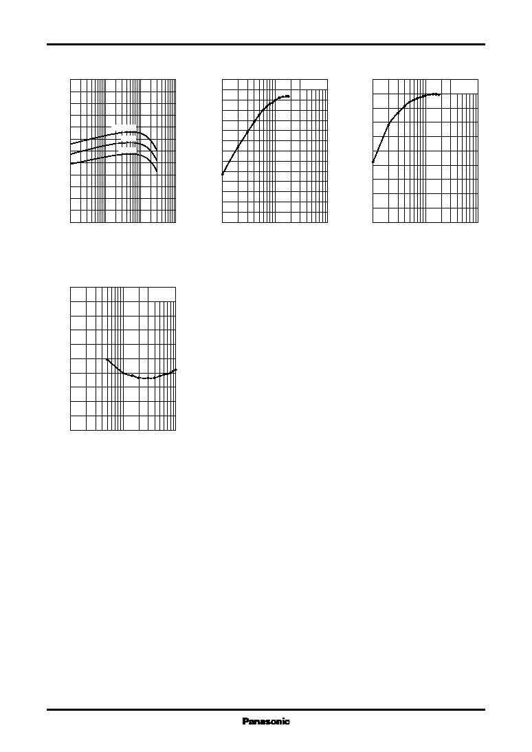
Electrical Characteristics
(Ta=25∞C)
Parameter
Collector cutoff current
Emitter cutoff current
Forward current transfer ratio
Collector output capacitance
Transition frequency
Noise figure
Foward transfer gain
Symbol
I
CBO
I
EBO
h
FE
C
ob
f
T
NF
| S
21e
|
2
Conditions
V
CB
= 9V, I
E
= 0
V
EB
= 1V, I
C
= 0
V
CE
= 3V, I
C
= 10mA
V
CB
= 3V, I
E
= 0, f = 1MHz
V
CE
= 3V, I
C
= 10mA, f = 2GHz
V
CE
= 3V, I
C
= 3mA, f = 1.5GHz
V
CE
= 3V, I
C
= 10mA, f = 2GHz
min
80
typ
0.4
12.0
1.8
8.9
max
1
1
200
Unit
µ
A
µ
A
pF
GHz
dB
dB
Unit: mm
1:Emitter
2:Collector
3:Emitter
EIAJ:SC≠82
4:Base
S-Mini Type Package
Marking symbol :
3A
2.1
±
0.1
2.0
±
0.1
0.3
+0.1
0
0.65
0.65
1.3
±
0.1
0.7
±
0.1
0.5
±
0.1
0
.2
0 to 0.1
1.25
±
0.10
0.425
0.425
0.15
+0.10
≠0.05
0.2
±
0.1