1
Transistor
Rank
Q
R
S
h
FE1
160 ~ 260
210 ~ 340
290 ~ 460
2SD1991A
Silicon NPN epitaxial planer type
For general amplification
Complementary to 2SB1320A
s
Features
q
High foward current transfer ratio h
FE
.
q
Low collector to emitter saturation voltage V
CE(sat)
.
q
Allowing supply with the radial taping.
s
Absolute Maximum Ratings
(Ta=25∞C)
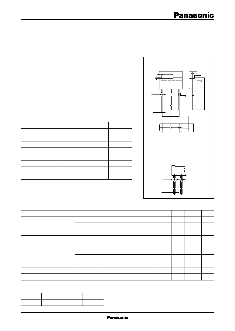
Unit: mm
Parameter
Collector to base voltage
Collector to emitter voltage
Emitter to base voltage
Peak collector current
Collector current
Collector power dissipation
Junction temperature
Storage temperature
1:Emitter
2:Collector
3:Base
MT1 Type Package
6.9
±
0.1
1.05
±
0.05
2.5
±
0.1
3.5
±
0.1
14.5
±
0.5
(1.45)
0.8
0.7
4.0
0.15
0.85
0.8
1.0
0.65 max.
0.45
+0.1
≠0.05
0.45
+0.1
≠0.05
2.5
±
0.5
2.5
±
0.5
2.5
±
0.1
1
2
3
Symbol
V
CBO
V
CEO
V
EBO
I
CP
I
C
P
C
T
j
T
stg
Ratings
60
50
7
200
100
400
150
≠55 ~ +150
Unit
V
V
V
mA
mA
mW
∞C
∞C
s
Electrical Characteristics
(Ta=25∞C)
Parameter
Collector cutoff current
Collector to base voltage
Collector to emitter voltage
Emitter to base voltage
Forward current transfer ratio
Collector to emitter saturation voltage
Transition frequency
Collector output capacitance
Symbol
I
CBO
I
CEO
V
CBO
V
CEO
V
EBO
h
FE1
*
h
FE2
V
CE(sat)
f
T
C
ob
Conditions
V
CB
= 20V, I
E
= 0
V
CE
= 20V, I
B
= 0
I
C
= 10
µ
A, I
E
= 0
I
C
= 2mA, I
B
= 0
I
E
= 10
µ
A, I
C
= 0
V
CE
= 10V, I
C
= 2mA
V
CE
= 2V, I
C
= 100mA
I
C
= 100mA, I
B
= 10mA
V
CB
= 10V, I
E
= ≠2mA, f = 200MHz
V
CB
= 10V, I
E
= 0, f = 1MHz
min
60
50
7
160
90
typ
0.1
150
3.5
max
1
1
460
0.3
Unit
µ
A
µ
A
V
V
V
V
MHz
pF
*
h
FE1
Rank classification
1.2
±
0.1
0.65
max.
0.45
0.1
0.05
+
≠
Note: In addition to the
lead type shown in
the upper figure, the
type as shown in
the lower figure is
also available.
(HW type)
2
Transistor
2SD1991A
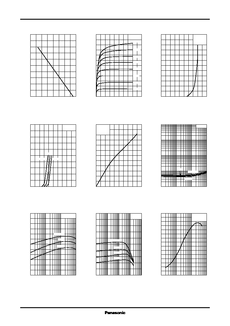
P
C
-- Ta
I
C
-- V
CE
I
B
-- V
BE
I
C
-- V
BE
I
C
-- I
B
V
CE(sat)
-- I
C
h
FE
-- I
C
h
FE
-- I
C
f
T
-- I
E
0
160
40
120
80
140
20
100
60
0
500
400
300
200
100
Ambient temperature Ta (∞C)
Collector power dissipation P
C
(mW
)
0
10
8
2
6
4
0
60
50
40
30
20
10
Ta=25∞C
I
B
=160
µ
A
40
µ
A
20
µ
A
60
µ
A
80
µ
A
140
µ
A
120
µ
A
100
µ
A
Collector to emitter voltage V
CE
(V)
Collector current I
C
(mA
)
0
1.0
0.8
0.2
0.6
0.4
0
1200
1000
800
600
400
200
V
CE
=10V
Ta=25∞C
Base to emitter voltage V
BE
(V)
Base current I
B
(
µ
A
)
0
2.0
1.6
0.4
1.2
0.8
0
200
160
120
80
40
V
CE
=10V
Ta=75∞C
≠25∞C
25∞C
Base to emitter voltage V
BE
(V)
Collector current I
C
(mA
)
0
1000
800
200
600
400
0
240
200
160
120
80
40
V
CE
=10V
Ta=25∞C
Base current I
B
(
µ
A)
Collector current I
C
(mA
)
0.1
1
10
100
0.3
3
30
0.01
0.03
0.1
0.3
1
3
10
30
100
I
C
/I
B
=10
25∞C
≠25∞C
Ta=75∞C
Collector current I
C
(mA)
Collector to emitter saturation voltage V
CE(sat)
(V
)
0.1
1
10
100
0.3
3
30
0
600
500
400
300
200
100
V
CE
=10V
Ta=75∞C
25∞C
≠25∞C
Collector current I
C
(mA)
Forward current transfer ratio h
FE
0.1
1
10
100
1000
0
1000
800
600
400
200
V
CE
=5V
Ta=125∞C
75∞C
25∞C
≠25∞C
Collector current I
C
(mA)
Forward current transfer ratio h
FE
≠ 0.1
≠1
≠10
≠100
≠ 0.3
≠3
≠30
0
300
240
120
180
60
V
CB
=10V
Ta=25∞C
Emitter current I
E
(mA)
Transition frequency f
T
(MHz
)
