ICs for Telephone
1
Publication date: November 2001
SDE00001BEB
AN1201SM
Polarity inverting charge pump DC/DC converter IC
I Overview
AN1201SM is a negative voltage generation IC for
bias voltage of transmission power module of cellular
phones. This IC is a polarity inverting DC/DC converter
to change from positive voltage into negative voltage.
I Features
· High power conversion efficiency: 89% typ. (when output
current is 5 mA.)
· Low output resistance: 20 typ.
· High voltage conversion efficiency: 99.9%
· Small (S-MINI) package
I Applications
· Cellular phones
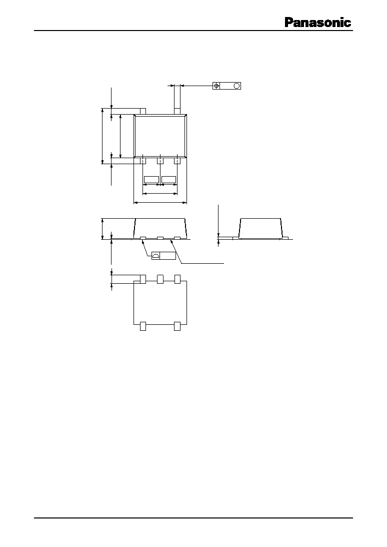
SMINI-5D
Unit: mm
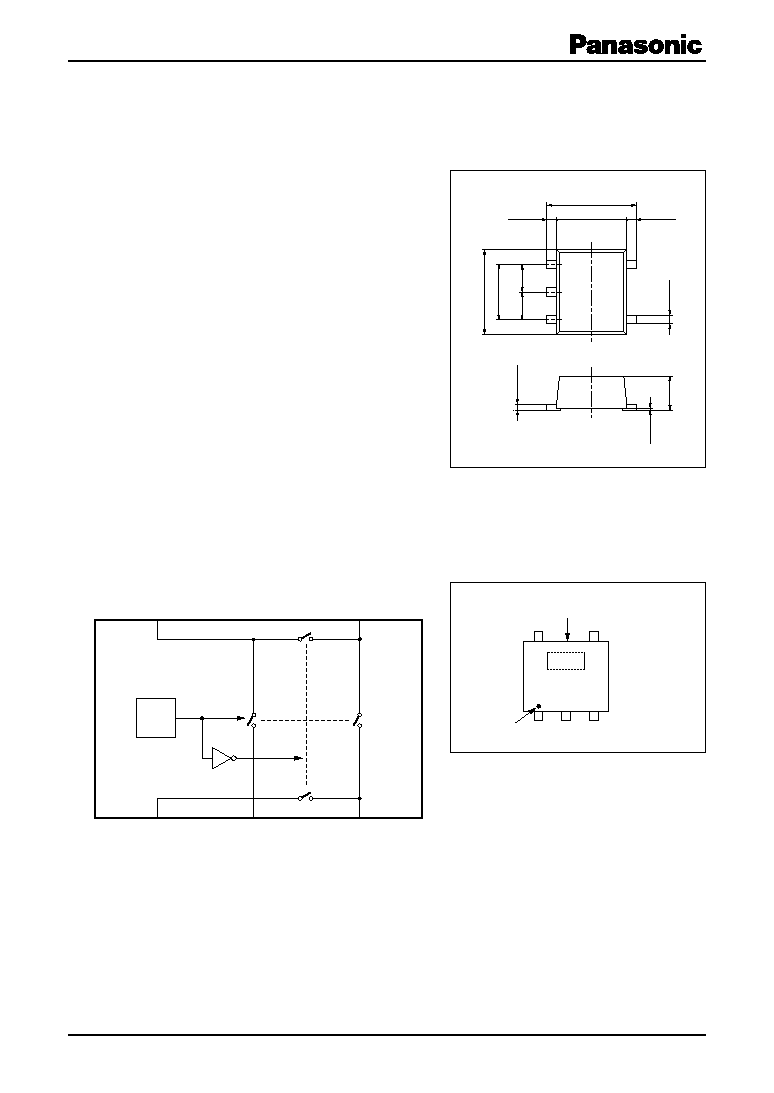
I Block Diagram
0 to 0.10
4
5
3
2
1
0.8
±0.10
0.15
±0.05
0.20
±0.05
2.10
±0.10
0.225
±0.05
1.65
±0.10
0.225
±0.05
2.00
±0.10
1.30
±0.10
0.65
±0.05
0.65
±0.05
C2
5
V
IN
1
V
OUT
2
GND
4
C1
3
S3
S1
S2
S4
OSC
· Marking
A L
Part No.: "AL" indicates AN1201SM.
Pin No.1 displayed
Note) The package of this product will be changed
to lead-free type (SMINI-5DA). See the new
package dimensions section later of this
datasheet.
AN1201SM
2
SDE00001BEB
Note) 1. Do not apply external currents or voltages to any pins not specifically mentioned.
For circuit currents, (
+) denotes current flowing into the IC, and (-) denotes current flowing out of the IC.
2. *1: Except for the power dissipation, operating ambient temperature and storage temperature, all ratings are for T
a
= 25°C.
*2: T
a
= 85°C, For the independent IC without a heat sink.
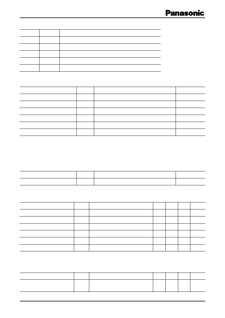
I Absolute Maximum Ratings
Parameter
Symbol
Rating
Unit
Supply voltage
V
IN
3.3
V
Supply current
I
IN
10
mA
Output current
I
O
20
mA
Power dissipation
*2
P
D
48
mW
Operating ambient temperature
*2
T
opr
-30 to +85
°C
Storage temperature
*1
T
stg
-55 to +125
°C
I Recommended Operating Range
Parameter
Symbol
Range
Unit
Supply voltage
V
IN
2.0 to 3.0
V
I Electrical Characteristics at V
IN
= 2.5 V, C1 = 1 µF, T
a
= 25°C
Parameter
Symbol
Conditions
Min
Typ
Max
Unit
Oscillator frequency
f
OSC
V
IN
= 2.5 V, no load
66
125
198
kHz
T
a
= -30°C to 85°C
· Design reference data
Note) The characteristics listed below are theoretical values based on the IC design and are not guaranteed.
Unless otherwise specified: V
IN
= 2.5 V, T
a
= 25°C
Parameter
Symbol
Conditions
Min
Typ
Max
Unit
Consumption current
I
CC
No load
0.25
1
mA
Oscillator frequency
f
OSC
No load
90
125
160
kHz
Output resistance
R
OUT
Load 500
50
Voltage conversion efficiency
V
No load
95.0
99.9
%
Power efficiency
P
Load 500
80
89
%
Consumption current in Sleep mode
I
OFF
V
IN
= 0.2 V, no load
1
µA
I Pin Descriptions
Pin No.
Symbol
Description
1
V
IN
Supply voltage pin
2
V
OUT
Inverted output pin
3
C1
Charge pump capacitor's positive polarity side connecting pin
4
GND
Ground pin
5
C2
Charge pump capacitor's negative polarity side connecting pin

Please read the following notes before using the datasheets
A. These materials are intended as a reference to assist customers with the selection of Panasonic
semiconductor products best suited to their applications.
Due to modification or other reasons, any information contained in this material, such as available
product types, technical data, and so on, is subject to change without notice.
Customers are advised to contact our semiconductor sales office and obtain the latest information
before starting precise technical research and/or purchasing activities.
B. Panasonic is endeavoring to continually improve the quality and reliability of these materials but
there is always the possibility that further rectifications will be required in the future. Therefore,
Panasonic will not assume any liability for any damages arising from any errors etc. that may ap-
pear in this material.
C. These materials are solely intended for a customer's individual use.
Therefore, without the prior written approval of Panasonic, any other use such as reproducing,
selling, or distributing this material to a third party, via the Internet or in any other way, is prohibited.
Request for your special attention and precautions in using the technical information
and semiconductors described in this material
(1) An export permit needs to be obtained from the competent authorities of the Japanese Govern-
ment if any of the products or technologies described in this material and controlled under the
"Foreign Exchange and Foreign Trade Law" is to be exported or taken out of Japan.
(2) The technical information described in this material is limited to showing representative character-
istics and applied circuit examples of the products. It does not constitute the warranting of industrial
property, the granting of relative rights, or the granting of any license.
(3) The products described in this material are intended to be used for standard applications or gen-
eral electronic equipment (such as office equipment, communications equipment, measuring in-
struments and household appliances).
Consult our sales staff in advance for information on the following applications:
· Special applications (such as for airplanes, aerospace, automobiles, traffic control equipment,
combustion equipment, life support systems and safety devices) in which exceptional quality and
reliability are required, or if the failure or malfunction of the products may directly jeopardize life or
harm the human body.
· Any applications other than the standard applications intended.
(4) The products and product specifications described in this material are subject to change without
notice for reasons of modification and/or improvement. At the final stage of your design, purchas-
ing, or use of the products, therefore, ask for the most up-to-date Product Standards in advance to
make sure that the latest specifications satisfy your requirements.
(5) When designing your equipment, comply with the guaranteed values, in particular those of maxi-
mum rating, the range of operating power supply voltage and heat radiation characteristics. Other-
wise, we will not be liable for any defect which may arise later in your equipment.
Even when the products are used within the guaranteed values, redundant design is recommended,
so that such equipment may not violate relevant laws or regulations because of the function of our
products.
(6) When using products for which dry packing is required, observe the conditions (including shelf life
and after-unpacking standby time) agreed upon when specification sheets are individually exchanged.
(7) No part of this material may be reprinted or reproduced by any means without written permission
from our company.
2001 MAR