New
R i p p l e F i l t e r I C A N 1 2 8 1 S S M
I
Overview
The AN1281SSM is a ripple filter IC that rejects the ripple component su-
perimposed on the regulator output. Use for the VCO bias of cellular phones
improves C/N and S/N.
I
Features
G
Small I/O voltage difference
G
The mounting area is reduced by adopting the SSmini-type package
I
Applications
G Cellular phones
and others
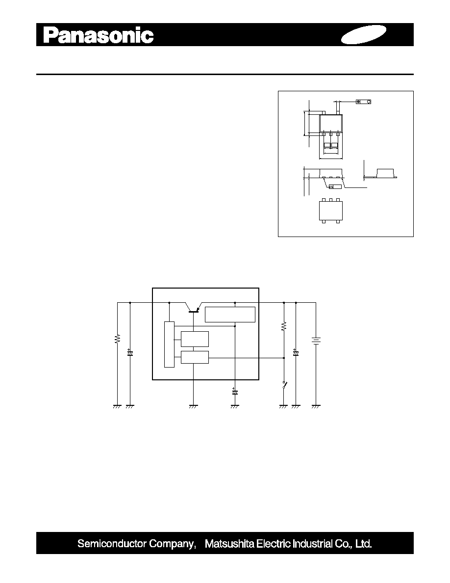
I
Block Diagram
1 Kotari-yakemachi, Nagaokakyo, Kyoto 617-8520, Japan
Tel. (075) 951-8151
http://www.panasonic.co.jp/semicon/
New publication, effective from Dec. 6. 2001
M00494AE
¶ The products and specifications are subject to change without any notice. Please ask for the latest product standards to guarantee the satisfaction of your product requirements.
4
3
5
2
1
3
4
0 to 0.10
2
1
5
0.20
0.20
1.20
±
0.10
1.60
±
0.10
1.00
±0.10
1.60
±0.10
0.50
Seating plane
0.60 max.
0.08
+0.10 -
0.05
0.20
+0.10
-0.05
0.50
0.10
M
0.10
Unit: mm
SSMINI-5DA(Lead-free package)
Constant
current
Switch
Load
V
oltage control
Starter/smoothing
circuit
3
V
IN
On/Off
CF
GND
5
V
OUT
4
1
2
4.7
µF
1
µF
0.1
µF
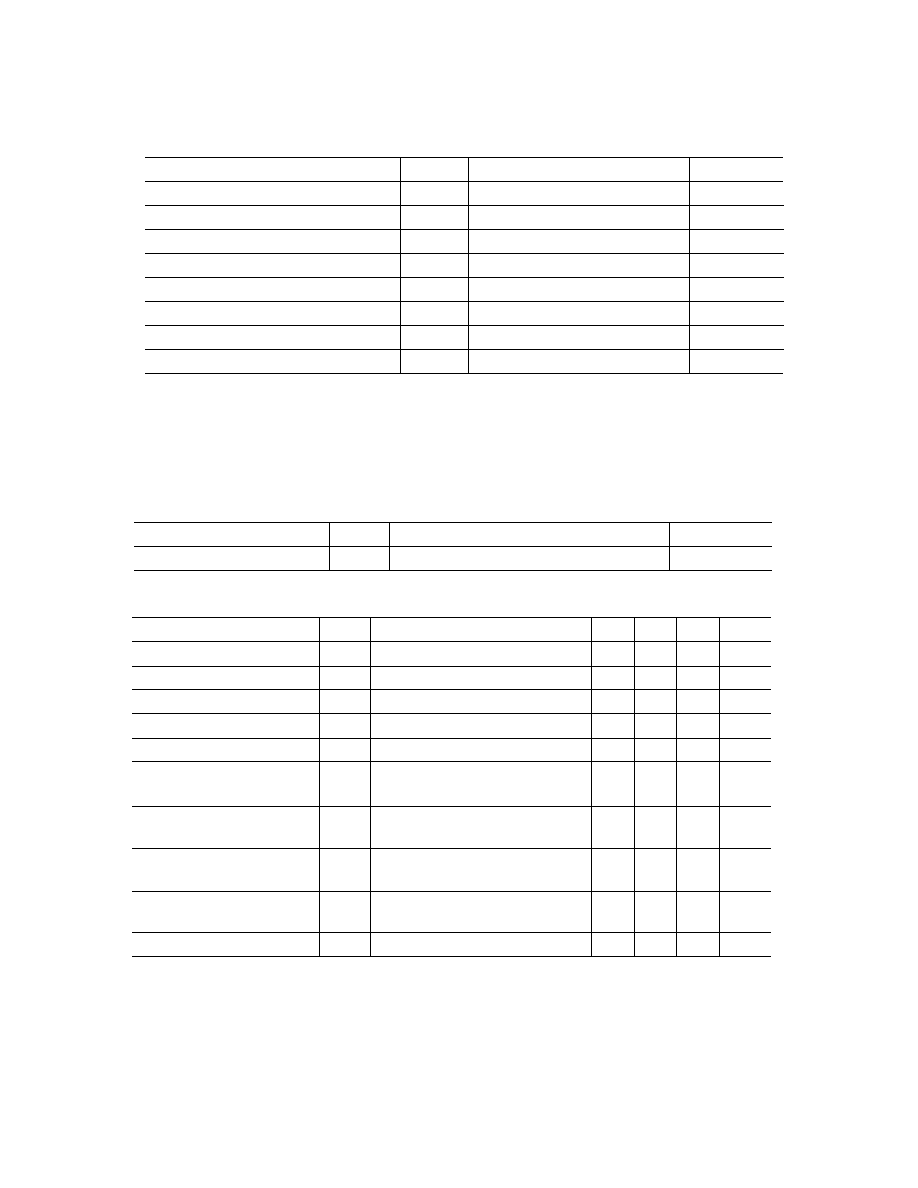
I Absolute Maximum Ratings
I Recommended Operating Range
Parameter
Symbol
Range
Unit
Supply voltage
V
CC
2.5 to 4.3
V
I Electrical Characteristics at T
a
= 25°C
Parameter
Symbol
Conditions
Min
Typ
Max
Unit
Output voltage 1
V
O1
V
IN
= 3.0 V, I
OUT
= -1
µA
2.62
2.82
V
Output voltage 2
V
O2
V
IN
= 3.0 V, I
OUT
= -15 mA
2.55
2.70
V
Consumption current 1
I
CC1
V
IN
= 3.0 V, I
OUT
= -1
µA
-735
-565
µA
Consumption current 2
I
CC2
V
IN
= 3.0 V, I
OUT
= -15 mA
-670
-515
µA
Load regulation
REG
L
V
IN
= 3.0 V, I
OUT
= -1
µA to -15 mA
0
120
220
mV
Consumption current against
I
REG
V
IN
= 3.0 V, I
OUT
= -1
µA to -15 mA
0
51
110
µA
load change
Ripple rejection ratio 1
RR
1
V
IN
= 3 V± 0.1 V, I
OUT
= -15 mA
26.5
29.5
dB
f = 1 kHz
Ripple rejection ratio 2
RR
2
V
IN
= 3 V± 0.1 V, I
OUT
= -15 mA
30.5
33.5
dB
f = 25 kHz
Ripple rejection ratio 3
RR
3
V
IN
= 3 V± 0.1 V, I
OUT
= -15 mA
26.5
29.1
dB
f = 100 kHz
Consumption current at off
I
OFF
V
IN
= 4.3 V, On/Off = 0 V
1
µA
Note) 1. Do not apply external currents or voltages to any pins not specifically mentioned.
For circuit currents, '+' denotes current flowing into the IC, and '-' denotes current flowing out of the IC.
2. *1: Except for the power dissipation, the operating ambient temperature and storage temperature, all ratings are for T
a
= 25°C.
*2: The power dissipation shown is the value for T
a
= 75°C.
*3: Do not over the supply voltage.
Parameter
Symbol
Rating
Unit
Supply voltage
V
IN
4.5
V
Supply current
I
CC
20
mA
Power dissipation
*2
P
D
60
mW
Operating ambient temperature
*1
T
opr
-25 to +75
°C
Storage temperature
*1
T
stg
-40 to +125
°C
Output current
I
O
-15
mA
Allowable application voltage for on/off pin
*3
V
ON/OFF
V
IN
V
Allowable maximum capacitance for CF pin
CF
10
µF