44-Pin QUADFLAT Package (QFP044-P-1010)
Unit:mm
34
44
12
22
33
23
1
11
10.0
±
0.3
10.0
±
0.3
0.8
0.35
±
0.1
12.3
±
0.4
2.0
±
0.2
0.9
±
0.25
0.9
±
0.25
+
0.1
≠ 0.05
0.15
12.3
±
0.4
(0.55)
0.1
±
0.1
GND
(DS)
34
33
35
32
31
29
26
28
27
24
4
21
5
6
22
25
20
19
17
23
16
18
8
7
11
14
9
10
12
13
3
15
2
1
44
43
42
40
41
39
36
38
30
37
GND
GND
V
CC
(Video)
V
CC
(DS)
Clamp
S.H
ALC
DET
ALCG
Amp
ALC
Amp
Clamp
WHD
MIX
AGC
Flicker
DC
F∑∑B
Pulse
Sep.
Vref
≠
Video
out
V.Sync
Mix
Low
Clip
C.BLK
Mix
H.Clip
Chara.
Mix
Chara.
Clamp
DC
F∑B
Amp
Mix
AP
Clamp
AP
Clip
Y.
Clamp
AP
Amp
AGC
OP
DC
F∑B
Y∑
Y∑
Cont
AGC
Det.
Clamp
+
≠
+
≠
+
Vref
Chara.
SW
s Overview
The AN2050FB is an integrated circuit specified to
the monochrome CCD image element which is em-
ployed in the monitoring video cameras, door phones,
TV telephone sets, etc. The high frequency block and
power block that are composed of 3-chip of DS signal
processing, AGC.
compensating and NTSC output
so far, are integrated into one chip to offer low cost.
s Features
∑ Frequency characteristics:10MHz (icompatible with
the CCD image element of 330,000 pixels)
∑ AGC range:18dB (improved SN ratio)
∑ Operating supply voltage range:4.5V to 5.3V (typ.
5V)
∑ Power consumption:typ. 225mW
AN2050FB
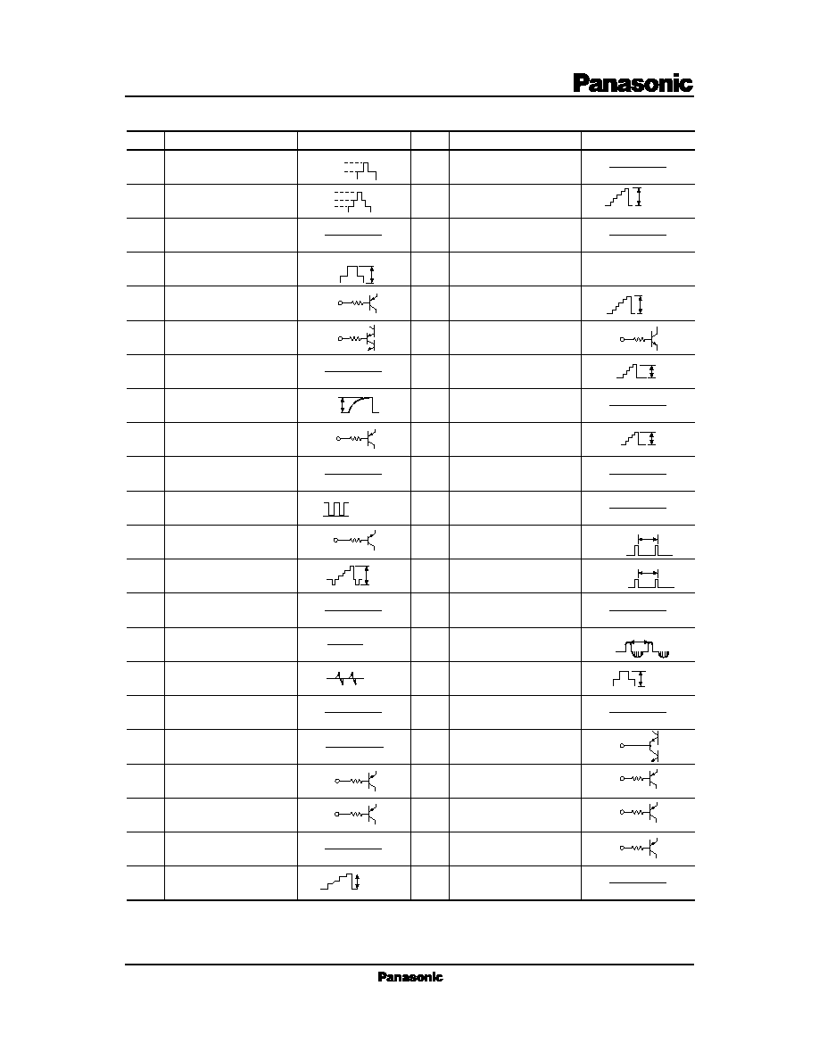
CCD Monochrome Video Camera Signal Processor IC
s Block Diagram
Parameter
Symbol
Rating
Unit
V
CC
I
CC
P
D
T
opr
T
stg
Power dissipation
Supply current
Supply voltage
Operating ambient temperature
Storage temperature
5.5
280
≠20 to +75
≠55 to +125
V
mW
∞C
∞C
mA
54
s Absolute Maximum Ratings (Ta=25∞C)
V
OB2
G
AGC1
OB control (1)
OB control (2)
AGC amp gain (1)
≠85
130
≠65
170
≠45
210
mV
PP
mV
PP
Parameter
min
Condition
typ
max
Unit
Symbol
G
AGC2
AGC amp gain (2)
16
19
22
dB
V
ALC
ALC DET output
500
600
700
mV
PP
G
1
circuit gain (1)
660
800
940
mV
PP
V
OB1
35
55
75
mV
PP
G
2
circuit gain (2)
550
mV
PP
V
AGC/DET
AGC DET output
400
480
560
mV
PP
G
CL1
AP clip (1)
0.9
1.1
1.4
V
PP
G
CL2
AP clip (2)
≠10
dB
G
Y
Y
amp gain
1.1
1.3
1.5
V
PP
I
25
Supply current (1)
26.5
31
35.5
mA
I
33
Supply current (2)
9.5
14
18.5
mA
V
CP1
CP1 pulse separation level
3.4
3.8
4.2
V
V
WHD
WHD pulse separation level
2.15
2.55
2.95
V
V
WBL
WBL pulse separation level
0.4
0.8
1.2
V
V
CP2
CP2 pulse separation level
3.1
3.5
3.9
V
V
BLK
V
CC
=5V
V
CC
=5V
V
CC
=5V
V
CC
=5V
V
CC
=5V
V
CC
=5V
V
CC
=5V
V
CC
=5V
V
CC
=5V
V
CC
=5V
V
CC
=5V
V
CC
=5V
V
CC
=5V
V
CC
=5V
V
CC
=5V
V
CC
=5V
V
CC
=5V
V
CC
=5V
BLK pulse separation level
0.6
1
1.4
V
s Electrical Characteristics (Ta=25∞C)
Parameter
Symbol
Range
Operating supply voltage range
V
CC
4.5V to 5.3V
s Recommended Operating Range (Ta=25∞C)