 | –≠–ª–µ–∫—Ç—Ä–æ–Ω–Ω—ã–π –∫–æ–º–ø–æ–Ω–µ–Ω—Ç: AN3117S | –°–∫–∞—á–∞—Ç—å:  PDF PDF  ZIP ZIP |

Other ICs for Video
1
AN3117S, AN3117SA
RF modulator IC for VCR and VDP
s
Overview
The AN3117S and AN3117SA are RF modulator ICs
for VCR and VDP. They provide excellent high frequency
characteristics by adopting the high performance RF os-
cillation circuit.
s
Features
∑
Excellent in higher harmonic characteristics of RF
∑
Excellent in higher harmonic characteristics of sound
sub-carrier by the 1 MIX system
∑
Sharp white clip characteristics
∑
Suitable RF-MOD IC for the USA and Japan specifica-
tions
∑
Video AM modulator
∑
RF carrier oscillator
∑
White clip
∑
Channel changeover SW
∑
Sound FM modulator
∑
ANT SW driver
∑
Carrier off SW
∑
Available also the SSOP package (0.65 mm pitch)
s
Applications
∑
Video deck, video disk player, set top box for CATV,
game machine
s
Block Diagram
SOP016-P-0225A
AN3117S
Unit: mm
SSOP016-P-0225A
AN3117SA
Unit: mm
1
8
0.5
±
0.2
(1.0)
0
∞
to 10
∞
16
5.0
±
0.2
4.4
±
0.2
6.4
±
0.3
1.2
±
0.2
0.1
±
0.1
9
0.65
(0.225)
0.22
+
0.10
-
0.05
0.15
+
0.10
-
0.05
Seating plane
0.3
(0
∞
to 10
∞
)
(0.15)
10.1±0.3
4.2±0.3
6.5±0.3
1
8
16
9
1.27
(0.605)
Seating plane
Seating plane
0.40±0.25
0.1±0.1
1.5±0.2
1
2
3
4
7
8
5
6
FM
mod.
Channel
SW
Pre
amp.
RF
OSC
Buff.
White
clip
Video
clamp
MIX
RF
amp.
ANT SW
driver
9
10
11
12
13
14
15
16
V
ideo in
RF out
GND
P/S Adj.
Audio in

AN3117S, AN3117SA
Other ICs for Video
2
Note) 1. Measure in USA 3-ch. unless otherwise specified.
2. *1: Video modulation coefficient ranks.
∑
Normal delivery for B to D ranks with embossed taping of 2 000 pcs per reel
∑
The rank can not be specified in your order.
Video modulation coefficient
73% to 79%
77% to 83%
81% to 87%
Sound modulation coefficient
23 kHz to 27 kHz
B
C
D
s
Pin Descriptions
Pin No.
Description
1
Ground pin
2
P/S adjustment pin
3
RF OSC control pin
4
SIF oscillation pin 1
5
SIF oscillation pin 2
6
Sound input pin
7
Channel changeover pin
8
SAW/LC oscillation changeover pin
Pin No.
Description
9
RF oscillator emitter pin 1
10
RF oscillator emitter pin 2
11
RF oscillator base pin
12
Power supply pin
13
Antenna switch driver changeover pin
14
Antenna switch driver pin
15
RF output pin
16
Video input pin
s
Absolute Maximum Ratings
Parameter
Symbol
Rating
Unit
Supply voltage
V
CC
6
V
Supply current
I
CC
60
mA
Power dissipation
*2
P
D
269
mW
Operating ambient temperature
*1
T
opr
-
20 to
+
75
∞
C
Storage temperature
*1
T
stg
-
55 to
+
150
∞
C
Note) *1: Except for the operating ambient temperature and storage temperature, all ratings are for T
a
=
25
∞
C.
*2: The power dissipation shown is for the IC package in free air at T
a
=
75
∞
C.
Parameter
Symbol
Range
Unit
Supply voltage
V
CC
4.5 to 5.5
V
s
Recommended Operating Range
Parameter
Symbol
Conditions
Min
Typ
Max
Unit
Current consumption
ITOT
V
CC
=
5 V, no video and sound input
18
22
26
mA
Video output level
VP
No video and sound input
83
85
87
dBm
Video modulation depth
*1
mV
Video input
=
0.625 V[p-p]
73
79
%
10-staircase wave
77
80
83
81
87
s
Electrical Characteristics at V
CC
=
5 V, T
a
=
25
∞
C

Other ICs for Video
AN3117S, AN3117SA
3
Parameter
Symbol
Conditions
Min
Typ
Max
Unit
Video output difference between
V
P
No video and sound input
-
2
0
2
dB
channels
Video modulation coefficient
m
V
Video input
=
0.625 V[p-p]
-
2
0
2
%
difference between channels
10-staircase wave
Maximum video modulation
m
Vmax
Video input
=
1.0 V[p-p]
88
93.5
97
%
coefficient
10-staircase wave
P/S ratio
V
PS
No video and sound input
9.5
12
14.5
dB
Sound modulation coefficient
f
FM
Sound input
=
245 mV[rms]
23
25
27
kHz
f
=
1 kHz, sine wave
Maximum sound modulation
f
Fmax
Sound input = 980 mV[rms]
3.6
4
4.4
coefficient
f
=
1 kHz, ratio with f
FM
Sound S/N
SN
S
No video input
55
63
dB
Sync. distortion
Sync
m
=
80% Full white signal
-
2.5
%
Differential gain
DG
m
=
80% Staircase wave
3
%
Differential phase
DP
m
=
80% Staircase wave
2
deg
Sound modulation distortion
THD
f
FM
= ±
25 kHz
0.3
%
Sound oscillation frequency
f
SIF
V
CC
=
5 V
4.50
MHz
Driver output voltage
ASV
V
CC
=
5 V, 13-pin open
0
V
at ANT SW on
RF carrier off
At ANT SW off
ASRV
V
CC
=
5 V, 13-pin 5 V
4.0
V
Driver output voltage
RF carrier on
Load current 15 mA
ANT SW
COFF
V
CC
=
5 V
0.25
V
RF carrier off voltage
ANT SW
CON
V
CC
=
5 V
1.25
V
RF carrier on voltage
Chroma beat
IM
P/S
=
12 dB, P/C
=
18 dB,
65
dB
P
=
66 dB
µ
, 3.58 MHz, sine wave
In-band beat
Beat
70
dB
Video input impedance
R
V
30
k
Sound input impedance
R
A
20
k
Video output level
V
PT
T
a
=
25
∞
C reference
±
2
dB
Temperature characteristics
T
a
=
-
10
∞
C to
+
70
∞
C
Video modulation coefficient
m
T
T
a
=
25
∞
C reference
±
3
%
Temperature characteristics
T
a
=
-
10
∞
C to
+
70
∞
C
Maximum video modulation coefficient
m
maxT
T
a
=
25
∞
C reference
87.5
%
Temperature characteristics
T
a
=
-
10
∞
C to
+
70
∞
C
Sound oscillation
f
ST
T
a
=
25
∞
C reference
±
10
kHz
Frequency stability
T
a
=
-
10
∞
C to
+
70
∞
C
s
Electrical Characteristics at V
CC
=
5 V, T
a
=
25
∞
C (continued)
Note) Measure in USA 3-ch. unless otherwise specified.
AN3117S, AN3117SA
Other ICs for Video
4
s
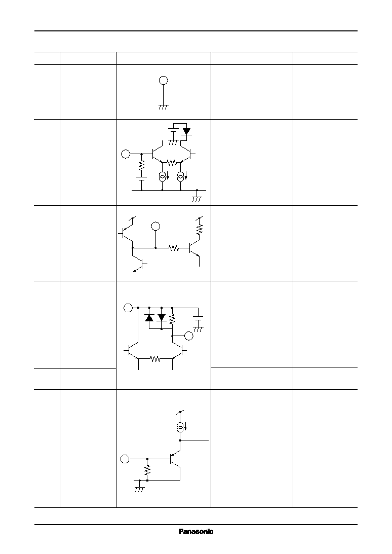
Terminal Equivalent Circuits
Pin No.
Pin name
Equivalent circuit
Description
Standard open voltage
1
GND
2
P/S
P/S ratio becomes large when
2.7 V
Adjustment pin
the capacitance connected be-
tween pin and GND increases.
3
RF OSC
Pin to control RF OSC.
Control pin
Oscillation of RF becomes
unstable when capacitance
connected between pin and
GND is too small.
4
SIF
Reference bias source of
4.2 V
Oscillation pin 1
oscillator. Sound buzz appears
to decrease in sense of hear-
ing when capacitance is con-
nected between pin and GND
to cut AC signal. Oscillation
frequency is determined by
the external tank circuit.
5
SIF
Reference oscillator for
4.2 V
Oscillation pin 2
4.5 MHz sound modulator.
6
Sound input pin
Typical DC voltage is almost
0 V
same as GND potential. If
DC level of sound input sig-
nal is GND potential, an ex-
ternal coupling capacitor is
not necessary. The circuit
configuration which is de-
signed to minimize the volt-
age variation at power sup-
ply on makes less pop noise.
1
2
2 k
3
10 k
4
5
6.2 k
6
20 k

Other ICs for Video
AN3117S, AN3117SA
5
s
Terminal Equivalent Circuits (continued)
Pin No.
Pin name
Equivalent circuit
Description
Standard open voltag
7
Channel switchover
The oscillation output comes
1.9 V
pin
out from pin 9 when the chan-
nel switchover pin is open,
and comes out from pin 10
when that pin is connected to
GND.
8
SAW/LC
Power output of RF oscillator
0.3 V
Oscillation switch-
increases if this pin is opened.
over pin
9
RF oscillator
Pin 9 and pin 10 are oscillator
4.0 V
emitter pin 1
output pins which configure
emitter output of NPN tran-
4.3 V
sistor.
10
RF oscillator
4.3 V
emitter pin 2
4.0 V
11
RF oscillator
Pin11 is input of oscillator
3.7 V
base pin
and impedance is 3 k
.
12
Power supply pin
7
6.3 k
4 k
8.6 k
8
2 k
2 k
9
10
11
3 k
12