 | ÐлекÑÑоннÑй компоненÑ: AN5290S | СкаÑаÑÑ:  PDF PDF  ZIP ZIP |
Äîêóìåíòàöèÿ è îïèñàíèÿ www.docs.chipfind.ru
ICs for TV
1
AN5290S
Antenna diversity IC for on-vehicle TV
s
Overview
The AN5290S is an on-vehicle television antenna-
diversity IC in which the noise detection circuit and an-
tenna changeover circuit are integrated on a single chip.
It is destined for NTSC/PAL system.
s
Features
·
Built-in vertical and horizontal synchronizing circuit
·
It outputs changeover pulse for noise canceler.
·
Built-in antenna changeover stop function
s
Applications
·
On-vehicle televisions
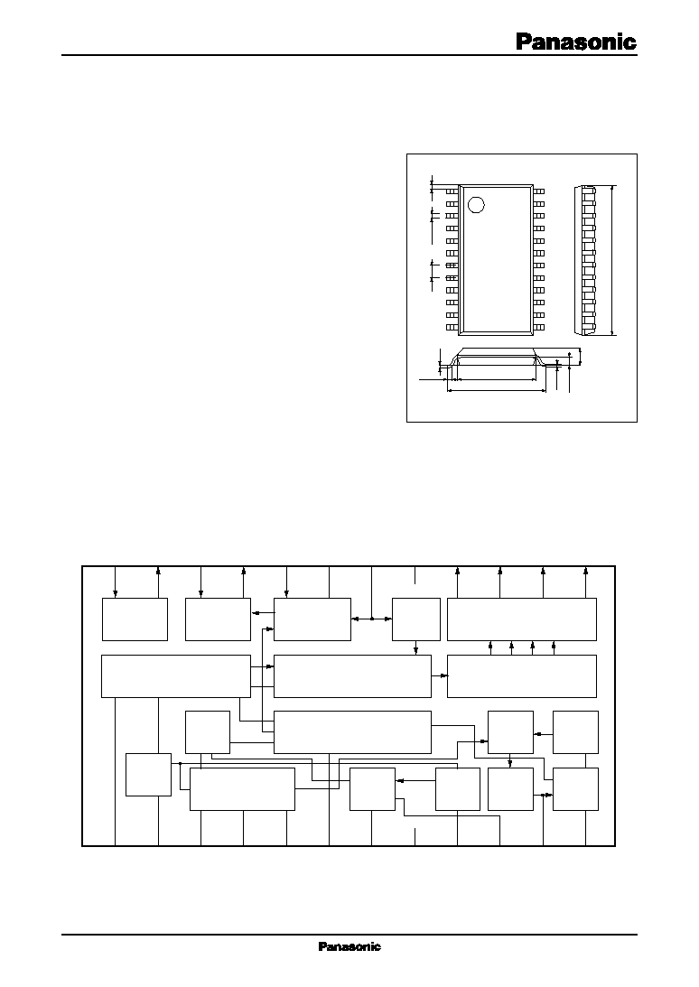
SOP024-P-0375A
Unit: mm
s
Block Diagram
1
0.4±0.25
0.45
1.27
0.1±0.1
0.3
7.2±0.3
9.4±0.3
0.15
0.925
2.0±0.2
15.3±0.3
2
4
5
6
9
10
11
12
7
8
13
14
15
16
17
18
19
20
21
22
23
24
3
24
23
22
21
20
19
18
17
V
CC
GND
16
15
14
13
1
2
3
4
5
6
7
8
9
10
11
12
1st noise
amp.
2nd noise
amp.
Noise
comparator
ANT
switch driver
ANT
select decoder
ANT
select control
ANT
switch control
ANT
choice
Diversity
On/Off
switch
1/12
divider
Phase
det.
Sync.
control
VCO
Charge
pump
V-sync.
sepa.
Vertical
OSC
Sync.
sepa.
Horizontal
OSC
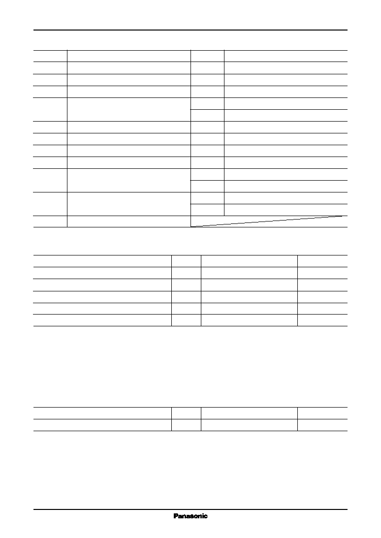
AN5290S
ICs for TV
2
Parameter
Symbol
Rating
Unit
Supply voltage
V
CC
5.6
V
Supply current
I
CC
30.0
mA
Power dissipation
*
P
D
168
mW
Operating ambient temperature
T
opr
-
30 to
+
80
°
C
Storage temperature
T
stg
-
55 to
+
125
°
C
Parameter
Symbol
Range
Unit
Supply voltage
V
CC
4.5 to 5.5
V
s
Recommended Operating Range
Note) 1. Except for the power dissipation, operating ambient temperature, and storage temperature, all ratings are for T
a
=
25
°
C.
2. In order to protect the IC, do not use the IC by rotating it 180 degrees.
3. To protect the IC, do not connect the open collector pins (pin 5, pin 6, pin 7, pin 13, pin 14, pin 15 and pin 16) directly to
the power supply. Use the protection resistors (1 k
or larger for pin 5, pin 6 and pin 7, and 200
or larger for pin 13, pin
14, pin 15 and pin 16). Use the IC within the range of its power dissipation.
4. * : T
a
=
80
°
C.
s
Absolute Maximum Ratings
s
Pin Descriptions
Pin No.
Description
1
Antenna selection level holding capacitance
2
Sync. separation video signal input
3
Horizontal sync. signal AFC output
4
Horizontal sync. signal oscillation time-
constant setting
5
Horizontal sync. signal output
6
Output for noise canceler
7
Vertical sync. signal output
8
GND
9
Vertical sync. signal separation time constant
setting
10
Vertical sync. signal oscillation time constant
setting
11
Charge pump integral time-constant setting
Pin No.
Description
12
VCO oscillation time-constant setting
13
Antenna selection output 4
14
Antenna selection output 3
15
Antenna selection output 2
16
Antenna selection output 1
17
Power supply
18
Noise comparator level setting/diversity off
19
Noise level hold capacitor
20
Noise comparator input
21
2nd noise amplifier output
22
Video clamp input
23
1st noise amplifier output
24
Video signal input
ICs for TV
AN5290S
3
s
Electrical Characteristics at V
CC
=
5 V, T
a
=
25
°
C
Parameter
Symbol
Conditions
Min
Typ
Max
Unit
Quiescent current without load
I
CC
Without input
12.0
20.0
28.0
mA
Horizontal sync. oscillation frequency
*
f
H
Without input, pin 5 frequency
15.58 15.68 15.78
kHz
PLL sync. oscillation frequency
12f
H
Without input, pin 12 frequency
186
188.2
190
kHz
Vertical sync. oscillation frequency
f
V
Without input, pin 7 frequency
36.0
42.0
48.0
Hz
Electric field judgment period
f
FJ
Without input, pin 21 frequency
36.0
42.0
48.0
Hz
Output frequency for N.C.
f
NC
Asynchronous, at changing over
36.0
42.0
48.0
Hz
antenna, pin 6 frequency
Antenna selection 1 on voltage
V
AS1ON
Voltage, when pin 16 is on
0.2
0.5
V
Antenna selection 1 off voltage
V
AS1OFF
Voltage, when pin 16 is off
4.9
5.0
V
Antenna selection 2 on voltage
V
AS2ON
Voltage, when pin 15 is on
0.2
0.5
V
Antenna selection 2 off voltage
V
AS2OFF
Voltage, when pin 15 is off
4.9
5.0
V
Antenna selection 3 on voltage
V
AS3ON
Voltage, when pin 14 is on
0.2
0.5
V
Antenna selection 3 off voltage
V
AS3OFF
Voltage, when pin 14 is off
4.9
5.0
V
Antenna selection 4 on voltage
V
AS4ON
Voltage, when pin 13 is on
0.2
0.5
V
Antenna selection 4 off voltage
V
AS4OFF
Voltage, when pin 13 is off
4.9
5.0
V
·
Design reference data
Note) The characteristics listed below are theoretical values based on the IC design and are not guaranteed.
Parameter
Symbol
Conditions
Min
Typ
Max
Unit
1st amplifier voltage gain
A
N1
V
IN
=
10 mV[p-p], f
IN
=
10 kHz,
17.0
dB
at 1st amp. active
2nd amplifier voltage gain
A
N2
V
IN
=
10 mV[p-p], f
IN
=
10 kHz,
17.5
dB
at 2st amp. active
Output voltage, when 2nd
V
NON2
At 2st amp. active,
1.51
V
amplifier is on
pin 21 DC voltage
Output voltage, when 2nd
V
NOF2
At 2nd amp. inactive,
4.20
V
amplifier is off
pin 21 DC voltage
Antenna input amplifier voltage
A
C
V
IN
=
50 mV[p-p], f
IN
=
10 kHz,
5.5
dB
gain
at input amp. active
Level hold output bias voltage
V
NOB2
At input amp. active,
1.43
V
pin 1 DC voltage
Antenna switch output sink
I
AS1
Antenna selection output pin,
10.0
mA
current 1
max. current, when pin 16 is on
Antenna switch output sink
I
AS2
Antenna selection output pin,
10.0
mA
current 2
max. current, when pin 15 is on
Antenna switch output sink
I
AS3
Antenna selection output pin,
10.0
mA
current 3
max. current, when pin 14 is on
Antenna switch output sink
I
AS4
Antenna selection output pin,
10.0
mA
current 4
max. current, when pin 13 is on
Note) * : The Horizontal oscillation frequency is a frequency after adjustment.
AN5290S
ICs for TV
4
s
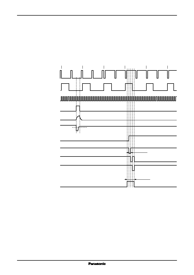
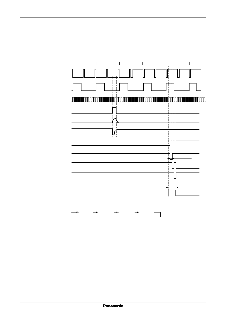
Technical Information
Note) The following characteristics are the reference value for design and not guaranteed value. The timing chart is for explaining
the IC operation plainly. Those vary depending on input condition.
1. Timing chart 1
·
When NTSC reception (in horizontal and vertical synchronization) antenna is selected.
Electric field judgment and antenna selection timing when the change over from ANT-1 to ANT-3 by the
antenna selection is done.
1st field video signal
Horizontal sync. signal
(pin 5)
VCO signal
(internal clock of IC)
Noise detection output
signal (pin 20)
Noise detection hold
(pin 19)
ANT-1 output
(pin 16)
ANT-2 output
(pin 15)
ANT-3 output
(pin 14)
ANT-4 output
(pin 13)
Selected antenna
ANT- 1 2 3 4 3
Output for N.C.
(pin 6)
(In the above timing chart, the 1st field video signal is not an internal signal but an
input signal, and some signals which do not outputted to pins, as VCO signal, are
included.)
Electric field judgment timing
(internal clock of IC)
5H
10.593
µ
s
5.296
µ
s
21.186
µ
s
(Electric field judgment level)
6H
7H
8H
9H
ICs for TV
AN5290S
5
s
Technical Information (continued)
2. Timing chart 2
·
When PAL reception (in horizontal and vertical synchronization) antenna is selected.
Electric field judgment and antenna selection timing when the change over from ANT-1 to ANT-3 by the
antenna selection is done.
1st field video signal
Horizontal sync. signal
(pin 5)
VCO signal
(internal clock of IC)
Noise detection output
signal (pin 20)
Noise detection hold
(pin 19)
ANT-1 output
(pin 16)
ANT-1 ANT-2 ANT-3 ANT-4
ANT-2 output
(pin 15)
ANT-3 output
(pin 14)
ANT-4 output
(pin 13)
Selected antenna
ANT- 1 2 3 4
Output for N.C.
(pin 6)
The antenna selection sequence is as follows:
Electric field judgment timing
(Internal clock of IC)
1H
10.667
µ
s
5.333
µ
s
21.333
µ
s
(Electric field judgment level)
2H
3H
4H
5H
6H