 | –≠–ª–µ–∫—Ç—Ä–æ–Ω–Ω—ã–π –∫–æ–º–ø–æ–Ω–µ–Ω—Ç: AN5295 | –°–∫–∞—á–∞—Ç—å:  PDF PDF  ZIP ZIP |
ICs for TV
1
AN5295NK
3-ch. sound signal processing single chip IC for TV (with I
2
C bus)
s
Overview
The AN5295NK is a television-use 3-ch. sound sig-
nal processing IC which incorporates volume, tone con-
trol (L/R/C 3-ch.), and surround sound, sound AGC,
lower sound enforce (L/R 2-ch.) functions. All of the func-
tions (including changeover switch) including external I/
O port can be controlled by I
2
C bus.
s
Features
∑
3-ch. of volumes can be controlled independently (max.
attenuation is 75 dB or more)
∑
Center output can be switched, ether center input or in-
side L
+
R signal (for HDTV)
∑
Lower sound enforce effect (frequency and gain) can be
adjusted with external parts
∑
With L
+
R output
s
Applications
∑
Television
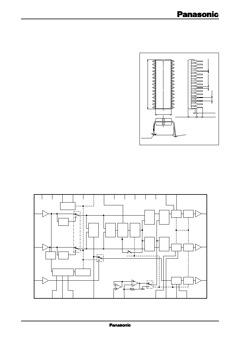
SDIP030-P-0400
Unit: mm
s
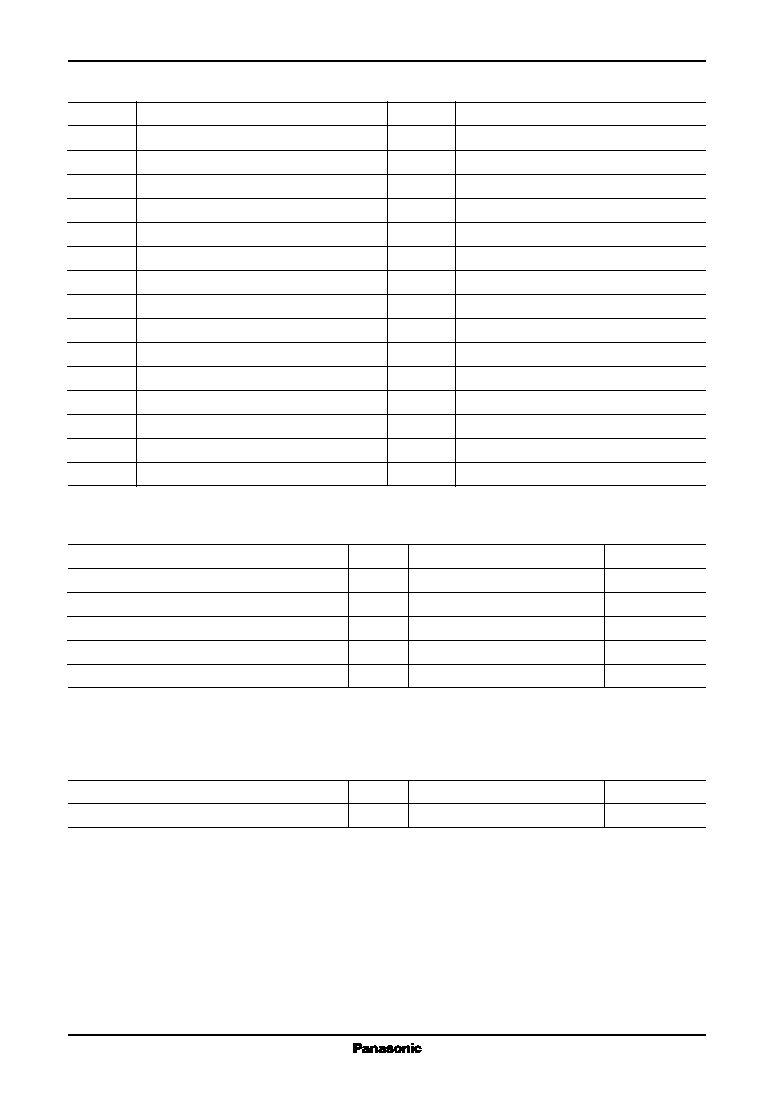
Block Diagram
3
∞
to 15
∞
26.7±0.3
0.5±0.1
1.0±0.25
3.3±0.25
4.7±0.25
1
15
30
16
0.35
≠0.05
+0.1
8.6±0.3
0.9±0.25
10.16±0.25
1.778
30
1
28
L-In
R-In
B-Out/
C-In
L-Out
R-Out
C-Out
19
11
18
29
2
15
14
6
17
7
8
12
13
16
25
23
3
4
5
27
26
24
9
10
21
20
A
GC Adj.
LS1
LS2
ADD
B-In
B-Gain
RB
RT
CB
CT
22
V
CC
GND
SD
A
SCL
V
REF
Extension I/O (H/L) DAC
1
PS
STB
SR
V
SL
V
SCV
STT
LB
LT
I
2
C
I
2
C
Loop
C-sel
Bass add
0 dB adj.
VCA
VCA
L
+
R
Vol.
Vol.
Buffer
Off
On
On
Off
Buffer
Buffer
Tone
Tone
Add
Add
L
+
S
R
-
S
LPF
amp.1
PS
1st
stage
L
-
R
L
+
R
Buffer
Vol.
+
mute
Buffer
Vol.
Tone
Buffer
Control
Level sense
On
Off
AN5295NK
ICs for TV
2
Parameter
Symbol
Rating
Unit
Supply voltage
V
CC
13.5
V
Supply current
I
CC
80
mA
Power dissipation
*2
P
D
1 143
mW
Operating ambient temperature
*1
T
opr
-
20 to
+
75
∞
C
Storage temperature
*1
T
stg
-
55 to
+
150
∞
C
Parameter
Symbol
Range
Unit
Supply voltage
V
CC
10.8 to 13.2
V
s
Recommended Operating Range
Note) *1: Except for the operating ambient temperature and storage temperature, all ratings are for T
a
=
25
∞
C.
*2: T
a
=
70
∞
C.
s
Absolute Maximum Ratings
s
Pin Descriptions
Pin No.
Description
1
R-ch. input pin
2
Ground pin
3
AGC 0 dB adjustment pin
4
AGC level sensor-1 pin
5
AGC level sensor-2 pin
6
1/2 V
CC
pin
7
Phase shift pin
8
L/R/C-ch. bass DAC output pin
9
R-ch. bass f
C
setting pin
10
R-ch. treble f
C
setting pin
11
R-ch. output pin
12
R-ch. volume DAC output pin
13
L-ch. volume DAC output pin
14
I
2
C communication clock pin
15
I
2
C communication data pin
Pin No.
Description
16
C-ch. volume DAC output pin
17
Extension DAC pin 1
18
C-ch. output pin
19
L-ch. output pin
20
C-ch. treble f
C
setting pin
21
C-ch. bass f
C
setting pin
22
L-ch. treble f
C
setting pin
23
L-ch. bass f
C
setting pin
24
Bass mix. gain adjustment pin
25
L/R/C-ch. treble DAC output pin
26
Bass detection LPF ope.-amp. input pin
27
L+R add after AGC output pin
28
C-ch. input pin
29
Power supply pin (12 V)
30
L-ch. input pin
ICs for TV
AN5295NK
3
s
Electrical Characteristics at T
a
=
25
∞
C
Parameter
Symbol
Conditions
Min
Typ
Max
Unit
Tone control
Volume max. level
*
V
VO (max)
V
IN
=
1 V[rms], f
=
1 kHz
-
2.3
-
0.3
1.7
dB
Volume typ. level
*
V
VO (typ)
V
IN
=
1 V[rms], f
=
1 kHz
-
16.2
-
13.2
-
10.2
dB
Volume min. level
*
V
VO (min)
V
IN
=
1 V[rms], f
=
1 kHz
-
75
dB
Bass: boost level
V
BB
V
IN
=
400 mV[rms], f
=
50 Hz
9.2
11.2
13.2
dB
Bass: cut level
V
BC
V
IN
=
400 mV[rms], f
=
50 Hz
-
11.7
-
9.7
-
7.7
dB
Treble: boost level
V
TB
V
IN
=
400 mV[rms], f
=
20 kHz
9.7
11.7
13.7
dB
Treble: cut level
V
TC
V
IN
=
400 mV[rms], f
=
20 kHz
-
12.1
-
10.1
-
8.1
dB
AGC
Input/output level 1
*
V
AGC1
V
IN
=
1 mV[rms], f
=
1 kHz
0.7
1.7
2.7
mV[rms]
Input/output level 2
*
V
AGC2
V
IN
=
50 mV[rms], f
=
1 kHz
70
110
150
mV[rms]
Input/output level 3
*
V
AGC3
V
IN
=
1 V[rms], f
=
1 kHz
275
345
415
mV[rms]
Circuit current
*
I
CC
V
IN
=
0 mV
25
45
65
mA
Total harmonics distortion
*
THD
V
IN
=
1 V[rms], f
=
1 kHz
0.1
0.5
%
Max. input voltage
*
V
IN (max)
THD
=
1%
2.8
V[rms]
Mute level
*
V
MUTE
V
IN
=
1 V[rms], f
=
1 kHz
-
80
dB
Noise level at volume max.
*
V
NO (max)
V
IN
=
0 mV, R
g
=
0
115
200
µ
V[rms]
Noise level at volume min.
*
V
NO (min)
V
IN
=
0 mV, R
g
=
0
45
100
µ
V[rms]
Surround level (max.)
*
V
SU (max)
V
IN
=
100 mV[rms], f
=
1 kHz
12.4
14.4
16.4
dB
Surround level (min.)
*
V
SU (min)
V
IN
=
100 mV[rms], f
=
1 kHz
2.9
4.9
6.9
dB
Surround level at loop on
*
V
LPSUL
V
IN
=
100 mV[rms], f
=
1 kHz
4.9
6.9
8.9
dB
Level at bass add on
*
V
BAONL
V
IN
=
400 mV[rms], f
=
50 Hz
3.95
5.95
7.95
dB
Cross talk
*
CT
V
IN
=
1 V[rms], f
=
1 kHz
-
70
-
68.5
dB
Channel balance
*
CB
V
IN
=
1 V[rms], f
=
1 kHz
-
1.5
0
1.5
dB
L
-
R volume tracking (1/4)
*
V
TR
V
IN
=
1 V[rms], f
=
1 kHz
-
2.0
0
2.0
dB
I
2
C interface
Sink current at ACK
I
ACK
Maximum value of pin 15 sink current
2.0
10
mA
at ACK
SCL, SDA signal high-level input
V
IHI
3.5
5.0
V
SCL, SDA signal low-level input
V
ILO
0
0.9
V
Max. allowable input frequency
f
Imax
100
kbit/s
Note) * : Uses DIN audio filter.
AN5295NK
ICs for TV
4
∑
Design reference data
Note) The characteristics listed below are theoretical values based on the IC design and are not guaranteed.
Parameter
Symbol
Conditions
Min
Typ
Max
Unit
I
2
C interface
Bus free before start
t
BUS
4.0
µ
s
Start condition setup time
t
SU. STA
4.0
µ
s
Start condition hold time
t
HD. STA
4.0
µ
s
Low period SCL, SDA
t
LO
4.0
µ
s
High period SCL
t
HI
4.0
µ
s
Rise time SCL, SDA
t
r
1.0
µ
s
Fall time SCL, SDA
t
f
0.35
µ
s
Data setup time (write)
t
SU. DAT
0.25
µ
s
Data hold time (write)
t
HD. DAT
0
µ
s
Acknowledge setup time
t
SU. ACK
3.5
µ
s
Acknowledge hold time
t
HD. ACK
0
µ
s
Stop condition setup time
t
SU. STO
4.0
µ
s
DAC
6-bit DAC DNLE
L
6
1 LSB
=
(data (max.)
-
data (00))/63
0.1
1.0
1.9
LSB/step
s
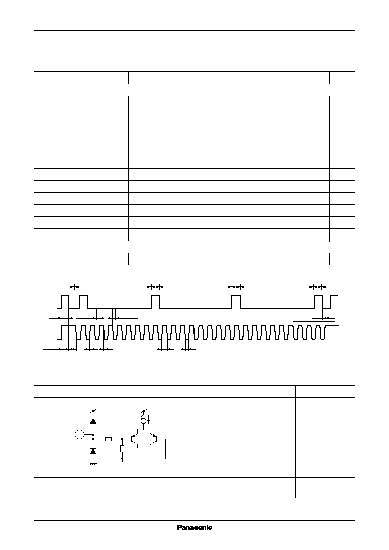
Electrical Characteristics at T
a
=
25
∞
C (continued)
t
BUF
Start
condition
SDA
SCL
Stop
condition
Slave address
Sub address
Data byte
ACK
ACK
ACK
t
SU. DAT
t
SU. STA
t
HDSTA
t
r
t
LO
t
SU. STO
t
HD. DAT
t
HI
t
f
t
LO
Pin No.
Equivalent circuit
Description
Voltage (V)
1
R-In:
6
R-ch. Input pin
2
GND:
0
GND pin
s
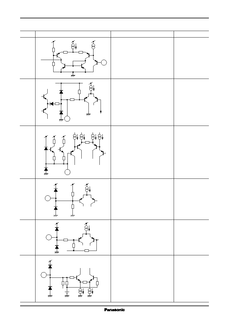
Terminal Equivalent Circuits
200
50 k
1/2 V
CC
1
ICs for TV
AN5295NK
5
s
Terminal Equivalent Circuits (continued)
Pin No.
Equivalent circuit
Description
Voltage (V)
3
AGC Adj.:
AGC on/off changeover
AGC off at 1.2 V or less.
4
LS1:
7
AGC level sensor 1
5
LS2:
0.5 to 1.5
AGC level sensor 1, 2
6
V
REF
:
6
Reference voltage to be stabilized
7
PS:
6
Phase shift pin
8
STB:
3
±
1
L/R/C-ch. bass DAC output pin
3
40 k
96 k
20 k
20 k
900
250
18 k
1/2 V
CC
4
5
430
CTL
Level 1
Level 2
20
k
50 k
50 k
6
200
18 k
7
18 k
500
500
20.5
k
20.5
k
3 V
8
5.8 k