 | ÐлекÑÑоннÑй компоненÑ: AN5308 | СкаÑаÑÑ:  PDF PDF  ZIP ZIP |
Äîêóìåíòàöèÿ è îïèñàíèÿ www.docs.chipfind.ru
ICs for TV
1
AN5308NK
Single chip IC for color TV (Built-in I
2
C bus interface)
s
Overview
The AN5308NK is an IC in which NTSC video,
chroma, RGB, sync. and deflection signal process-
ing circuits are integrated on a single chip incorpo-
rating I
2
C bus controller.
s
Features
·
Video block
: Built-in wide band width filter,
pre-shoot and over-shoot
amount adjustment, aperture
changeover possible and with
ABL pin
·
Chroma block
: Built-in ACC filter and with
color difference output pin
·
RGB block
: With color difference signal
input pin and analog RGB
·
Sync. block
: With sync. BLK in/output pin,
µ
changeover and H center
adjustment possible
·
Deflection block: Built-in screen distortion
correction circuit
s
Applications
·
TV
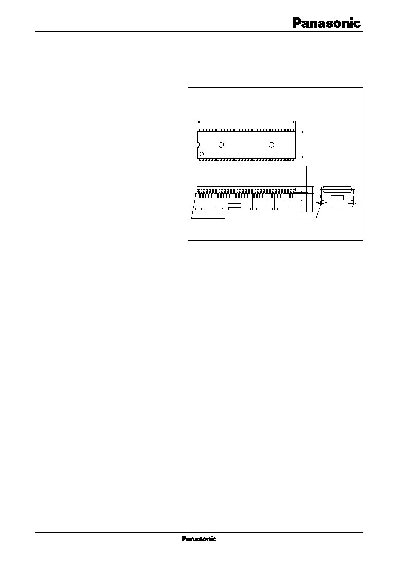
SDIP064-P-0750B
Unit: mm
64
33
1
32
1.778
19.05
0.25
+0.1
0.05
0.5
+0.1
0.05
0
°
to 15
°
5.2 max.
0.7 min.
(3.3)
3.85±0.2
17.0±0.2
(1.0)
(1.641)
Seating plane
58.4±0.3
AN5308NK
ICs for TV
2
46
Blooming le
v
e
l
47
APL det.
48
White max. det.
50
Black min. det.
51
AC
L
52
Y
-in
53
Slv
. add.
54
55
Sync. in
56
B
.
P.
P.
i
n
57
Sync. in
58
Lock det.
59
S.C.P
. in
60
S.C.P
. out
61
FBP in
62
V
-pulse
63
AFC1
Sharpness
control
64
Sync./Def.
GND
1
2f
H
VCO
2
Key stone
filter
3
AFC2
4
X-ray
5
X-ray-ref
6
H-out
7
6.3 V
9
SDA
10
I
2
C GND
11
SCL
12
AGC
13
Ramp
14
Feed back
15
V-out
17
9 V
16
Parabola
18
9 V
19
R-out
20
Corner
gain cont.
21
G-out
22
B-out
24
EHT in
25
Y
S
in
26
B-in
27
Corner
slice v
ol.
28
G-in
29
R-in
30
B
-
Y in
31
R
-
Y in
32
V/C/RGB GND
33
R
-
Y out
35
B
-
Y out
36
3.58 VCO
37
APC f
ilter
38
CW out
40
Killer f
ilter
41
42
Color
track
43
ABL
44
C-in
45
5 V
49
Y-clamp
Y
-clamp
Y
-
delay
line
Y
-delay
line(1)
Aperture
control
delay
50 ns
Aperture control
delay(1)
IRE
V
oltage
lmp.trs
V
oltage1
Aperture
control
delay
125 ns
Aperture
control
delay
125 ns
Aperture
control
delay
50 ns
Sharpness
Y
-clamp
Pre Ov
er
Contrast
control
Contrast
(7
+
1)
Sharpness(7)
Bright
DC tra
(1)
Bright(8)
Bright
Pedestal
APL
det.
Bright
min.det.
Bright
control
Black
APL
Black slice
(3
+
SW)
Service SW
(1)
60 IRE
det.
Black
gain(4)
Corner
control
EW corner 1
(3)
SW corner(2)
T
rapezoidal
correction(6)
V
ertical linearity(6)
V
ertical amplitude(7)
V
ertical S-curv
e(6)
V
ertical EHT(4)
EW parabola(6) Horizontal EHT(4)
Ramp
P
arabola
V
ertical
position(6)
V
ertical amp. polarity
(1)
H-center
(5)
Service SW(1)
EW amp.
V/I
Con
v
erter
H-sync.
sep.
Under 60
cont.
30/60
cont.gain
IRE
gain
Burst
cont.
Color/Black
le
v
el correction
selection
(1)
cont.
gain
(4)
le
v
e
l
(4)
White
max.det.
BLK PLS
(1)
SW
Neck
AFC1
AFC gain
(1)
VCO
V count
do
wn
S.C.P
SCP selection(1)
BGP2
AFC2
I
2
C
/
DAC
Lock det.
H Count
do
wn
Cut of
f B
(8
+
2)
Dri
v
e
2
(7
+
SW)
Dri
v
e
1
(7
+
SW)
On Screen
On Screen
BLK
On Screen
B
Dri
v
e
(Pulse)
Dri
v
e
B
Cut of
f
BLK
Cut of
f
(B-clamp)
Cut
of
f
B
V
-amp.
Shut/Hold
do
wn
Po
wer
On/Of
f
H.V
.sync.
sep.
Cut of
f G
(8)
Mute(1)
On Screen
G
Dri
v
e
G
Cut of
f
(G-clamp)
Cut
of
f
G
Cut of
f R
(8
+
2)
On Screen
R
Dri
v
e
R
Dri
v
e
White
White character slice(4)
White character correction(4)
VCO
APC
Bias2
DEMOD
Killer
Phase shift
Color track
Color track ON/OFF
(1)
AC
C
det.
AC
C
amp.2
AC
C
amp.1
G
-
Y
matrix
G
-
Y
Ratio
DEMAXIS
(1)
DEMAXIS
(2)
T
int (1)
T
int (7)
T
int (2)
Clamp
(1)
Clamp
(2)
Color control
Color (7
+
1)
Demodulate
shift(5)
Demodultae
Gain(6)
Color control
Cut of
f
(R-clamp)
Cut
o
f
f
R
RGB
matrix
(2)
RGB
matrix
(1)
RGB
matrix
(3)
s
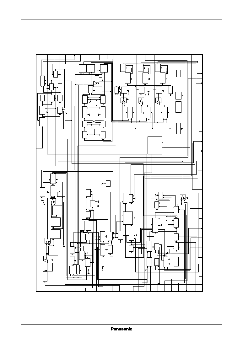
Block Diagram
ICs for TV
AN5308NK
3
s
Pin Descriptions
Pin No.
Description
35
R
-
Y output
36
B
-
Y output
37
3.58 MHz VCO
38
Chroma APC filter
40
VCO output
41
Killer filter
42
Color track filter
43
ABL input
44
Chroma input
45
5 V power supply (V
CC2
)
46
Blooming level input
47
APL detection use filter
48
White detection use filter
49
Y-clamp
50
Black detection filter/color control
51
ACL input
52
Y-signal input
53
Slave address changeover
54
V-sync. sep. filter
55
H-sync. input
56
Black detection inhibition pulse input
57
V-sync. input
58
Lock det. filter
59
Sandcastle pulse input
60
Sandcastle pulse output
61
Flyback pulse (FBP) input
62
V-pulse output
63
AFC1 filter
64
Sharpness control output
8, 23, 34, 39
Non-connection
Pin No.
Description
1
Sync., Def. GND
2
503 kHz VCO
3
Vertical position transition DAC output
4
AFC2 filter
5
High-tention detection input (X-ray)
6
High-tention detection reference voltage
7
Horizontal drive pulse output
9
Horizontal power supply (H V
CC
)
10
I
2
C SDA input
11
I
2
C GND
12
I
2
C SCL input
13
Reference ramp wave form AGC
14
Reference ramp wave form generation
15
Corner slice level
16
Sync. 9 V power supply
17
Vertical deflection sawtooth wave output
18
EW output
19
9 V power supply (V
CC1
)
20
R-output
21
Corner gain control
22
G-output
24
B-output
25
EHT voltage detection
26
Y
S
input
27
On-screen B-input
28
Corner slice volume
29
On-screen G-input
30
On-screen R-input
31
B
-
Y input
32
R
-
Y input
33
V/C/RGB GND
AN5308NK
ICs for TV
4
Parameter
Symbol
Conditions
Min
Typ
Max
Unit
DC characteristics
Supply current
I
16
+
19
V
CC1
: 9 V, V
CC2
: 5 V, pin 9: 12 V
74
90
106
mA
with 380
Supply current
I
45
V
CC1
: 9 V, V
CC2
: 5 V, pin 9: 12 V
59
71
83
mA
with 380
Sync. input pin voltage
V
55
-
1
V
CC1
: 9 V, V
CC2
: 5 V, pin 9: 12 V
0.8
1.3
1.8
V
with 380
Sync. input pin voltage
V
57
-
1
V
CC1
: 9 V, V
CC2
: 5 V, pin 9: 12 V
0.8
1.3
1.8
V
with 380
Video input pin voltage
V
7
-
33
V
CC1
: 9 V, V
CC2
: 5 V, pin 9: 12 V
2.7
3.2
3.7
V
with 380
ABL input pin voltage
V
43
-
33
V
CC1
: 9 V, V
CC2
: 5 V, pin 9: 12 V
2.5
3.0
3.5
V
with 380
ACL input pin voltage
V
51
-
33
V
CC1
: 9 V, V
CC2
: 5 V, pin 9: 12 V
2.5
3.0
3.5
V
with 380
Blooming level pin voltage
V
46
-
33
V
CC1
: 9 V, V
CC2
: 5 V, pin 9: 12 V
2.2
2.7
3.2
V
with 380
Chroma input pin voltage
V
44
-
33
V
CC1
: 9 V, V
CC2
: 5 V, pin 9: 12 V
1.5
2.0
2.5
V
with 380
s
Absolute Maximum Ratings
Parameter
Symbol
Rating
Unit
Supply voltage
V
CC
V
CC1
9.6
V
V
CC2
5.6
Supply current
I
CC
I
CC1
(I
16
+
I
19
)
113
mA
I
CC2
(I
45
)
89
I
9
26
Power dissipation (T
a
=
70
°
C)
P
D
947
mW
Operating ambient temperature
*1
T
opr
-
20 to
+
70
°
C
Storage temperature
*1
T
stg
-
55 to
+
150
°C
Note) *1: Except for the operating ambient temperature and storage temperature, all ratings are for T
a
=
25
°
C.
Parameter
Symbol
Range
Unit
Supply voltage
V
CC1
8.5 to 9.0 to 9.5
V
V
19
-
1
,
11
,
33
V
CC2
4.5 to 5.0 to 5.5
V
V
45
-
1
,
11
,
33
Supply current
I
9
15 to 20 to 25
mA
s
Recommended Operating Range
s
Electrical Characteristics at T
a
=
25
°
C
ICs for TV
AN5308NK
5
Parameter
Symbol
Conditions
Min
Typ
Max
Unit
DC characteristics (continued)
B
-
Y output pin voltage
V
31
-
33
V
CC1
: 9 V, V
CC2
: 5 V, pin 9: 12 V
2.3
2.8
3.3
V
with 380
R
-
Y output pin voltage
V
32
-
33
V
CC1
: 9 V, V
CC2
: 5 V, pin 9: 12 V
2.3
2.8
3.3
V
with 380
Horizontal signal processing
Horizontal stabilized supply voltage
HV
CC
V
CC1
: 9 V, V
CC2
: 5 V, pin 9: 12 V
5.9
6.3
6.7
V
with 380
Constant voltage operating resistance
RHV
CC
I
9
: 15 mA to 25 mA
30
Horizontal free-running oscillation
f
HO-1
15.434 15.734 16.034
kHz
frequency 1
Horizontal free-running oscillation
f
HO
-
2
At hold down
16.3
16.4
16.8
kHz
frequency 2
Variation of f
HO
, when supply
f
HO
f
HO
frequency difference, when
0
100
200
Hz
voltage start-up
V
CC3
other power supply off
on
Horizontal output pulse duty cycle
H
O
Hold down off
34.4
37.5
40.6
%
Horizontal output starting voltage
V
fH(S)
f
=
10 kHz to 20 kHz, when horizontal
5.2
V
oscillation voltage is 1 V[p-p] or more
Horizontal output level
V
fH
2.4
2.9
3.4
V
Horizontal pull-in range
f
PH
f
HO
=
15.73 kHz
±
400
Hz
H-center changeable range 1
T
DH
Phase lead of 1A[10]
[00]
1.8
2.5
3.2
µ
s
H-center changeable range 2
T
DH
Phase lead of 1A[10]
[1F]
-
3.0
-
2.3
-
1.6
µ
s
Lock detector output voltage 1
V
58
-
M
Synchronous
5.1
5.8
6.5
V
Lock detector output voltage 2
V
58
-
L
Asynchronous
-
0.1
0
0.5
V
Lock detector output voltage 3
V
58
-
T
Hold down
7.6
8.3
9.0
V
Burst gate pulse width
T
BGP
Sandcastle output
1.8
2.5
3.2
µ
s
Sandcastle pulse output level
V
BGP
V
CC
: typ.
4.0
4.3
4.6
V
(BGP)
Sandcastle pulse output level
V
HBLK
V
CC
: typ.
2.7
3
3.3
V
(HBLK)
Sandcastle pulse output level
V
VBLK
V
CC
: typ.
1.2
1.5
1.8
V
(VBLK)
Vertical signal processing
Vertical output pulth width
V
O
360
380
400
µ
s
Vertical output level
V
62H
3.8
4.3
4.8
V
Vertical output free-running frequency
f
VO
58.8
60.0
61.2
Hz
Vertical blanking pulse width
VBLK
1.09
1.12
1.15
ms
s
Electrical Characteristics at T
a
=
25
°
C (continued)