 | –≠–ª–µ–∫—Ç—Ä–æ–Ω–Ω—ã–π –∫–æ–º–ø–æ–Ω–µ–Ω—Ç: AN5392FBQ | –°–∫–∞—á–∞—Ç—å:  PDF PDF  ZIP ZIP |
ICs for TV
1
AN5392FBQ
Luminance and color difference drive/cutoff signal processor IC
with I
2
C bus
s
Overview
The AN5392FBQ is an RGB processor IC which
converts the luminance and color difference signal into a
primary color signal. This IC supports all kinds of input
signal from hi-vision, wide, NTSC, PAL, VGA, etc. for
maximum rationalization and high performance of the
end products.
s
Features
∑
A wider band signal processing (Y: 30 MHz/
-
3 dB,
color difference: 15 MHz/
-
3 dB)
∑
High picture quality thanks to a large variety of built-in
correction circuit for Y signal
∑
Y, C
-
Y signal conversion circuit built in for RGB signal
for a personal computer
∑
Possible to mount in a high density thanks to SMD pack-
age
s
Applications
∑
Hi-vision TV, wide TV, projection TV, plasma display
panel (PDP)
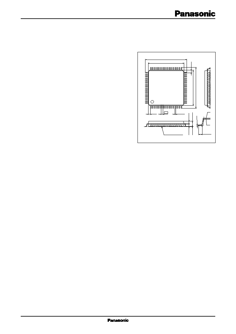
QFS064-P-1414
Unit: mm
16.2±0.3
14.0±0.2
16.2±0.3
(1.0)
14.0±0.2
0.9±0.1
0.9±0.1
1.95±0.2
0.1±0.1
48
33
1
16
64
49
17
32
(1.0)
0.35
+0.10
≠0.05
0
.15
+0.10
≠0.05
Seating plane
0.8
0.55±0.2

AN5392FBQ
ICs for TV
2
s
Block Diagram
48
47
46
45
44
43
42
41
40
39
38
37
36
35
34
33
DC re
genaration rate
Analog V
CC
Blooming le
v
el in
Black peak det.
White peak det.
APL det.
R-CLP
G-CLP
B-CLP
OSD-R in
OSD-G in
OSD-B in
Y
S
in
Y
M
in
R, G, B limiter in
Spot killer in
I
2
L GND
R,G,B GND
B
-
Y out
Y
-out
R
-
Y out
CLP (R, G, B) in
R-in
G-in
B-in
R, G, B
V
CC
V
P
in
Sla
v
e
address SW
SD
A
SCL
I
2
L V
CC
Pulse GND
1
2
3
4
5
6
7
8
9
10
11
12
13
14
15
16
17
18
19
20
21
22
23
24
25
26
27
28
29
30
31
32
BLK in
R,G,B mute
Neck mute
CRT mute
DI in
Pulse V
CC
Analog GND
R-GND
R-out
R-V
CC
B-GND
B-out
B-V
CC
G-GND
G-out
G-V
CC
Y, U, V GND
B
-
Y (M2) in
Y (M2) in
R
-
Y (M2) in
CLP (M2) in
B
-
Y (M1) in
Y (M1) in
R
-
Y (M1) in
CLP (M1) in
M/S in
Y, U, V V
CC
B
-
Y (S) in
Y (S) in
R
-
Y (S) in
ABL/ACL in
VM out
64
63
62
61
60
59
58
57
56
Input
block
55
54
53
52
51
50
49
BLK
block
Output
block
Video
block
Chrominance
block
R, G, B
Y, U, V
block
I
2
C DAC
block
SW
block
Matrix
block
ABL/ACL
block
Y
Y
G
B
R
G
-
Y
B
-
Y
R
-
Y
B
-
Y
R
-
Y
G
B
R
ICs for TV
AN5392FBQ
3
s
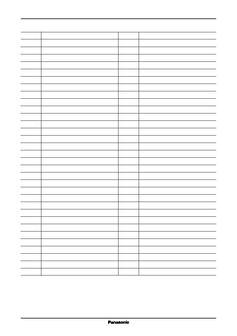
Pin Descriptions
Pin No.
Description
1
I
2
L GND
2
R, G, B GND
3
B
-
Y output
4
Y-output
5
R
-
Y output
6
CLP (R, G, B) input
7
R-input
8
G-input
9
B-input
10
R, G, B V
CC
11
V
P
input
12
Slave address SW
13
SDA
14
SCL
15
I
2
L V
CC
16
Pulse GND
17
BLK input
18
R, G, B mute input
19
Neck mute input
20
CRT mute input
21
DI input
22
Pulse V
CC
23
Analog GND
24
R-GND
25
R-output
26
R-V
CC
27
B-GND
28
B-output
29
B-V
CC
30
G-GND
31
G-output
32
G-V
CC
Pin No.
Description
33
Spot killer input
34
R, G, B limiter input
35
Y
M
input
36
Y
S
input
37
OSD-B input
38
OSD-G input
39
OSD-R input
40
B-CLP filter
41
G-CLP filter
42
R-CLP filter
43
APL detection filter
44
White peak detection filter
45
Black peak detection filter
46
Blooming level input
47
Analog V
CC
48
DC regenaration rate
49
VM output
50
ABL/ACL input
51
R
-
Y (S) input (Pr (S) input)
52
Y (S) input
53
B
-
Y (S) input (Pb (S) input)
54
Y, U, V V
CC
55
M/S input
56
CLP (M1) input
57
R
-
Y (M1) input (Pr (M1) input)
58
Y (M1) input
59
B
-
Y (M1) input (Pb (M1) input)
60
CLP (M2) input
61
R
-
Y (M2) input (Pr (M2) input)
62
Y (M2) input
63
B
-
Y (M2) input (Pb (M2) input)
64
Y, U, V GND
AN5392FBQ
ICs for TV
4
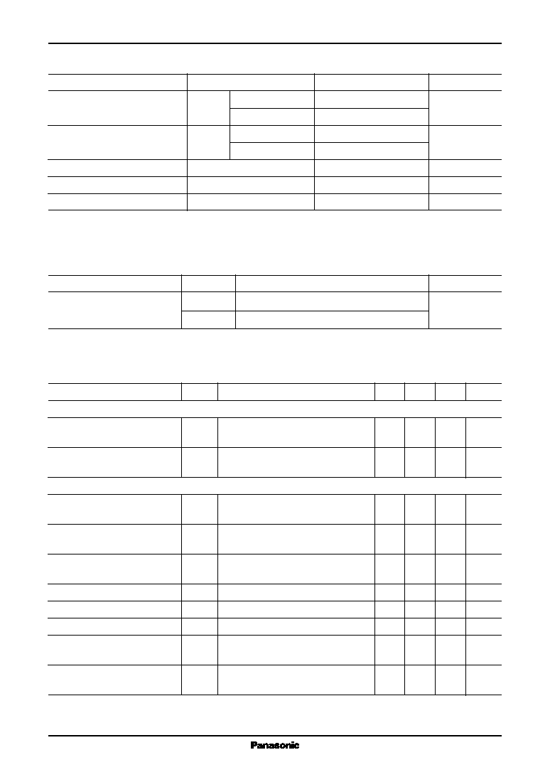
Parameter
Symbol
Rating
Unit
Supply voltage
V
CC
V
CC1
10.0
V
V
CC2
5.6
Supply current
I
CC
I
CC1
70.0
mA
I
CC2
34.0
Power dissipation
*2
P
D
685
mW
Operating ambient temperature
*1
T
opr
-
20 to
+
70
∞C
Storage temperature
*1
T
stg
-
55 to
+
150
∞C
s
Absolute Maximum Ratings
Note) *1: Except for the operating ambient temperature and storage temperature, all ratings are for T
a
=
25
∞
C.
*2: The power dissipation P
D
shown is for the independent IC without a heat sink in the free air at T
a
=
70
∞
C.
s
Absolute Maximum Ratings
Parameter
Symbol
Range
Unit
Supply voltage
V
CC1
8.1 to 9.9
V
V
CC2
4.5 to 5.5
s
Recommended Operating Range
Parameter
Symbol
Conditions
Min
Typ
Max
Unit
DC characteristics
Circuit current 1
*1
I
CC1
V
CC1
=
9 V, V
CC2
=
5 V
39
51
63
mA
No signal input
Circuit current 2
*1
I
CC2
V
CC1
=
9 V, V
CC2
=
5 V
20
25
30
mA
No signal input
Y-system
Video voltage gain
AY
G
Input: Sine wave 0.2 V[p-p]
4.7
5.6
6.7
Times
f
=
1 MHz, contrast: max.
Video voltage gain
AY
Ratio between R,G and B
-
2.5
0
+
2.5
dB
variation amount
Drive: typ.
Frequency characteristics
f
Y
Input: Sine wave 0.2 V[p-p]
-
6
-
3
+
1
dB
f
=
30 MHz, contrast: max.
Typical output pedestal
DC
P
Brightness: typ.
2.6
3.0
3.4
V
Brightness variable range
V
BR
Brightness: min.
max.
1.8
2.2
2.6
V
Contrast ratio
A
CON
Contrast: min.
max.
25
30
dB
APL detection voltage
V
APL
Input: Total white 0.7 V[0-p]
0.7
1.0
1.3
V
APL detection pin 43 voltage
APL detection ratio
APL
Input: Total white 0.7 V[0-p]
0.35 V[0-p] 0.46
0.54
0.66
Times
APL detection pin 43 voltage ratio
s
Electrical Characteristics at V
CC1
=
9 V, V
CC2
=
5 V, T
a
=
25
∞
C
Note) *1: I
CC1
is a total amount of the current flowing through pin 10, pin 26, pin 29, pin 32, pin 47 and pin 54.
I
CC2
is a total amount of the current flowing through pin 15 and pin 33.
ICs for TV
AN5392FBQ
5
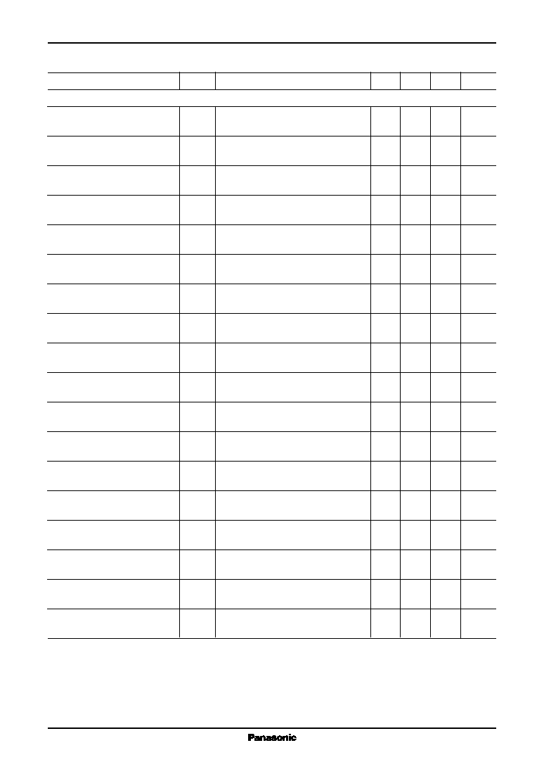
Parameter
Symbol
Conditions
Min
Typ
Max
Unit
Y-system (continued)
DC regeneration ratio 1
DC
1
Input signal: APL 10%
90%,
96
102
107
%
APL det. pin 0 V
DC regeneration ratio 2
DC
2
Input signal: APL 10%
90%,
65
75
85
%
DC regeneration SW/on, polarity:
-
DC regeneration ratio 3
DC
3
Input signal: APL 10%
90%,
115
125
135
%
DC regeneration SW: On, polarity:
+
Output blooming level
V
BL
Blooming DC
=
3.8 V,
5.7
6.7
7.7
V
pin 43: 0 V, brightness: max.
Output blooming level
V
BL
Blooming DC
=
3.8 V
4.2 V,
-
1.18
-
0.93
-
0.68
V
variation amount
pin 43: 0 V, brightness: max.
White gradation correction 1
*2
Y
1
Gain: max., level: typ.
max.
9.0
14
18.0
%
White gradation SW: On
White gradation correction 2
*2
Y
2
Gain: max., level: typ.
min.
-
24
-
18
-
12
%
White gradation SW: On
Black extension
Y
BL1
Output amplitude: 0 V[p-p]
-
0.1
0
+
0.1
V
characteristics 1
*3
Level: typ., gain: min.
max.
Black extension
Y
BL2
Output amplitude: 1.0 V[0-p]
-
0.49
-
0.37
-
0.25
V
characteristics 2
*3
Level: typ., gain: min.
max.
Black extension
Y
BL3
Output amplitude: 2.2 V[0-p]
-
0.1
0
+
0.1
V
characteristics 3
*3
Level: typ., gain: min.
max.
Black extension
Y
BL4
Black detection: Open
3 V
-
1.10
-
0.82
-
0.55
V
characteristics 4
*4
Level: typ., gain: typ.
Black extension
Y
BL5
Black detection: Open
3 V
-
2.00
-
1.55
-
1.00
V
characteristics 5
*4
Level: typ., gain: max.
Black extension
Y
BL6
Black detection: Open
3 V
-
0.48
-
0.30
-
0.12
V
characteristics 6
*4
Level: min.
max., gain: typ.
White character correction 1
*2
V
W1
Blooming DC adjustment
10.0
25.0
40.0
%
Level: max., gain: min.
typ.
White character correction 2
*2
V
W2
Blooming DC adjustment
-
9.3
0
9.3
%
Level: min., gain: min.
max.
White character correction off
*2
W
OFF
P
R
, P
B
input:
+
0.2 V[p-p]
-
0.2
0
+
0.2
V
Level: max., gain: min.
max.
ABL off
*5
V
ABL1
ABL/ACL pin: 7.5 V
-
0.1
0
+
0.1
V
Level: min., gain: min.
max.
ABL start 1
*5
V
ABL2
ABL/ACL pin: 3 V
0.28
0.39
0.50
V
Level: min.
max., gain: max.
s
Electrical Characteristics at V
CC1
=
9 V, V
CC2
=
5 V, T
a
=
25
∞
C (continued)
Note) *2: Control a blooming DC voltage (pin 46)
*3: Black gradation SW: On
*4: Black gradation SW: On, brightness: max.
*5: ABL SW: On, brightness: max.