 | ÐлекÑÑоннÑй компоненÑ: AN5693K | СкаÑаÑÑ:  PDF PDF  ZIP ZIP |
Äîêóìåíòàöèÿ è îïèñàíèÿ www.docs.chipfind.ru
ICs for TV
1
AN5693K
Luminance,Chroma and Sync. Signals Processing IC(with Built-in I
2
C-
bus Interface)for PAL/NTSC Color-TV
s
Overview
The AN5693K is an IC that processes PAL-and NTSC-
compatible video,chroma,RGB and sync. signals.
s
Features
·
Built-in I
2
C-bus control interface.
·
SECAM-compatible together with the AN5637 SECAM
signal processing IC.
s
Applications
·
TV(Multi-system compatible)
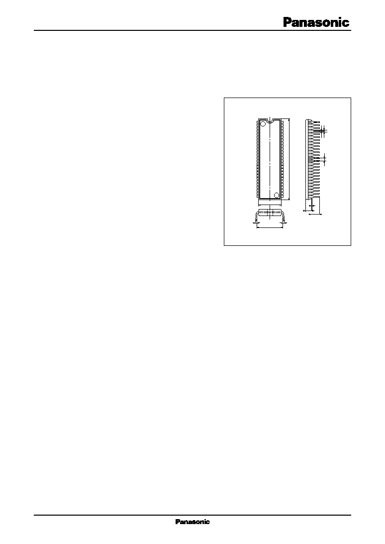
SDIP052-P-0600A
Unit : mm
1
26
27
52
47.7±0.3
13.7±0.3
(15.24)
3 to 15°
3 to 15°
(0.7)
3.85±0.3
(3.3)
1.778
0.5±0.1
1.0±0.25
2
AN5693K
ICs for TV
s
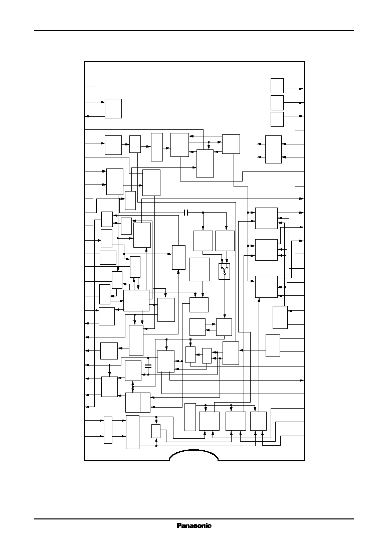
Block Diagram
*4-bit
*7-bit
*1-bit
*1-bit
*4-bit
*7
-
b
it
*2-bit
*1-bit
*6-bit
*7-bit
*1-bit
*1-bit
*8-bit
*7-bit
*Dri
v
e
8-bit
*Cut of
f 9-bit
*1-bit
27
28
Video In
N.C.
29
Video Out
30
BL Det.
Y In
31
32
Ver. Clamp
33
Ver. Sync. In
34
Hor. Sync. In
36
GND(VCJ)
35
V
CC3
(VCJ)
5V
51
52
39
V
CC2
40
AFC2
41
AFC1
42
Hor. VCO
43
X-ray
44
H-Out
45
50/60Hz Det. Out
46
V-Out
47
SECAM
48
-
(B
-
Y)Out
49
-
(R
-
Y)Out
-
(B
-
Y)In
-
(R
-
Y)In
50
SCP
38
FBP In
37
C In
CV
clamp
V
ideo
adjust
Hor
.
sync. sep.
Ve
r
.
BGP
sync. sep.
LPF
Y
contrast
Y
DAC out
I
2
C b
u
s
interf
ace
dri
v
e
cut of
f
B
BPF
Chroma SW
NTSC
BPF
PA
L
SW
System
FF
1H
det.
AC
C
T
int
APC
amp.
AC
C
generate
CW
HVBLK
HBLK
SCP
HVCO
dri
v
e
cut of
f
R
cut of
f
G
SW out
clamp
Black
e
xpansion
T
rap
Ext.
DAC
1
*9-bit
Ext.
DAC
2
*7-bit
Ext.
DAC
3
Sharpness
(Service)
Hor
.
lock det.
Hor
.
AFC2
AFC1
re
g.
count
do
wn
50/60Hz
(50/60Hz)
detect
Killer
ident
Hor
.
count do
wn
Ve
r
.
demod
B-Y
demod
Brightness
+
/
-
R-Y
contrast
Chroma
Saturation
out
Ve
r
.
SW
PN/S
do
wn
Shut
clamp
R-Y
clamp
G-Y
clamp
B-Y
G-Y
1
R-Clamp
2
G-Clamp
3
B-Clamp
4
Killer
5
Killer Out
6
APC
7
VCO 4.43MHz
8
VCO 3.58MHz
9
Spot Killer
10
Y
S
11
12
13
14
V
CC1
9V
15
R-Out
Y
S
pulse
Chroma
VCO
16
G-Out
17
B-Out
R-In
G-In
B-In
18
Lock Det.
19
GND(RGB)
20
ACL
21
SDA
22
SCL
23
GND(Ext. DAC)
24
25
26
Ext. DAC3
Ext. DAC2
Ext. DAC1
(8-bit)
3
ICs for TV
AN5693K
s
Pin Descriptions
Pin No.
Description
1
(R
-
Y)Clamp
2
(G
-
Y)Clamp
3
(B
-
Y)Clamp
4
Killer Filter
5
Killer Output
6
Chroma APC Filter
7
Chroma VCO 4.43 MHz
8
Chroma VCO 3.58 MHz
9
Spot Killer
10
Y
S
Input(Fast Blanking)
11
External R Input
12
External G Input
13
External B Input
14
V
CC1
15
R Output
16
G Output
17
B Output
18
Hor. Lock Detect
19
GND(RGB/I
2
C/DAC)
20
ACL
21
SDA
22
SCL
23
GND(EXT DAC)
24
External DAC 1 DC
25
External DAC 2 DC
26
External DAC 3 DC
Pin No.
Description
27
N.C.
28
Video Level Adjust Input
29
Video Level Adjust Output
30
Black Level Det/Blank Off SW
31
Y Input
32
Ver. Sync. Clamp
33
Ver. Sync. Input
34
Hor. Sync. Input
35
V
CC3
(Chroma/Jungle/DAC)
36
Chroma Input/Black Exp. Start
37
GND(Video/Chroma/Jungle)
38
FBP Input
39
V
CC2
(Hor. Stability Supply)
40
Hor. AFC 2 Filter
41
Hor. AFC 1 Filter
42
Hor. VCO(32 f
H
)
43
X-Ray Protection Input
44
Hor.Pulse Output
45
Ver. 50/60 Hz Detect Output
46
Ver. Pulse Output
47
SECAM Interface/CW Output
48
-
(B
-
Y)Output
49
-
(R
-
Y)Output
50
Sandcastle Pulse Output
51
-
(B
-
Y)Input
52
-
(R
-
Y)Input
4
AN5693K
ICs for TV
s
Absolute Maximum Ratings
Parameter
Symbol
Rating
Unit
Power supply voltage
V
CC
V
CC1
(14)
10.5
V
V
CC3
(35)
6.0
Power supply current
I
CC
I
14
77
mA
I
35
119
I
39
27
Power dissipation
*2
P
D
1 372
mW
Operating ambient temperature
*1
T
opr
-
20 to
+
70
°
C
Storage temperature
*1
T
stg
-
55 to
+
150
°
C
s
Recommended Operating Range
Parameter
Symbol
Range
Unit
Operating supply voltage range
V
CC1
8.1 to 9.9
V
V
CC3
4.5 to 5.5
Operating supply pin voltage
V
5
0 to 6
V
V
9
0 to V
14
V
10
0 to 6
V
11
0 to 6
V
12
0 to 6
V
13
0 to 6
V
21
0 to 6
V
22
0 to 6
V
24
0 to V
14
V
25
0 to V
14
V
36
0 to V
14
V
38
0 to V
47
V
43
0 to 2
V
45
0 to 6
V
47
0 to V
14
Note) *1 : The temperature of all items shall be T
a
=
25
°
C, except storage temperature and operating ambient temperature.
*2 : Power dissipation is at T
a
=
70
°
C(Refer to "Technical information")
Note) Do not apply voltage or current externally to any pin not listed in this table.
As for circuit current,(
+
)is the current flowing into the IC and(
-
)is the current flowing out of the IC.
5
ICs for TV
AN5693K
s
Electrical Characteristics at T
a
=
25
°
C
Parameter
Symbol
Conditions
Min
Typ
Max
Unit
Power supply DAC data is standard.
Supply current 1
I
14
Current when V
14
=
9 V
38
48
58
mA
Supply current 2
I
35
Current when V
35
=
5 V
48
60
72
mA
Steady state supply voltage
V
39
When Pin39 current
5.8
6.5
7.2
V
I
=
15 mA,Pin39 voltage
Steady state supply Current
I
39
Current when V
39
=
5 V
2
5
7
mA
Steady state supply input
R
39
DC measurement input resistance when
1
5
10
resistance
I
39
=
10 mA
25 mA
Interface
Video adjust gain
V
PO
DC measurement 20 log
output(0A
=
F8)
5
6
7
dB
output(0A
=
08)
Video adjust output resistance
R
O29
DC measurement
70
120
170
External DAC 1 DC voltage V
EXT1max
Pin24 DC voltage when DAC 0C
=
00
3.10
3.40
3.70
V
(max.)
DC measurement
External DAC 1 DC voltage V
EXT1min
Pin24 DC voltage when DAC 0C
=
7F
2.10
2.40
2.70
V
(min.)
DC measurement
External DAC 2 DC voltage V
EXT2max
Pin25 DC voltage DAC 0B
=
00,04D7
=
0
7.8
8.1
8.7
V
(max.)
DC measurement
External DAC 2 DC voltage V
EXT2min
Pin25 DC voltage DAC 0B
=
FF,04D7
=
1
0.1
0.8
1.0
V
(min.)
DC measurement
s
Recommended Operating Range
Parameter
Symbol
Range
Unit
Operating supply circuit current
I
39
10 to 25
mA
I
15
-
6.0 to
+
0.6
I
16
-
6.0 to
+
0.6
I
17
-
6.0 to
+
0.6
I
28
-
0.3 to
+
0.1
I
29
-
2.4 to
+
0.8
I
33
-
0.8 to
+
0.1
I
34
-
0.8 to
+
0.1
I
44
-
6.4 to
+
0.1
I
46
-
0.8 to
+
0.1
I
47
-
0.3 to
+
0.1
Note) Do not apply voltage or current externally to any pin not listed in this table.
As for circuit current,(
+
)is the current flowing into the IC and(
-
)is the current flowing out of the IC.