 | ÐлекÑÑоннÑй компоненÑ: AN6123 | СкаÑаÑÑ:  PDF PDF  ZIP ZIP |
Äîêóìåíòàöèÿ è îïèñàíèÿ www.docs.chipfind.ru
ICs for Telephone
1
AN6123MS
Speech network IC with ALC
s
Overview
The AN6123MS is an ALC IC for level control of
audio signal (300 Hz to 3 kHz).
Adopting a mini 5-pin package, mounting on a small
area is possible.
s
Features
·
Wide supply voltage operation range of V
CC
=
2.4 V to
6.0 V
·
Small current consumption of I
CC
=
500
µ
A
·
Reduction of a bad effect by the external noise thanks to
a package for a rear side mounting.
s
Applications
·
Cordless telephone, PDC, PHS telephone
s
Block Diagram
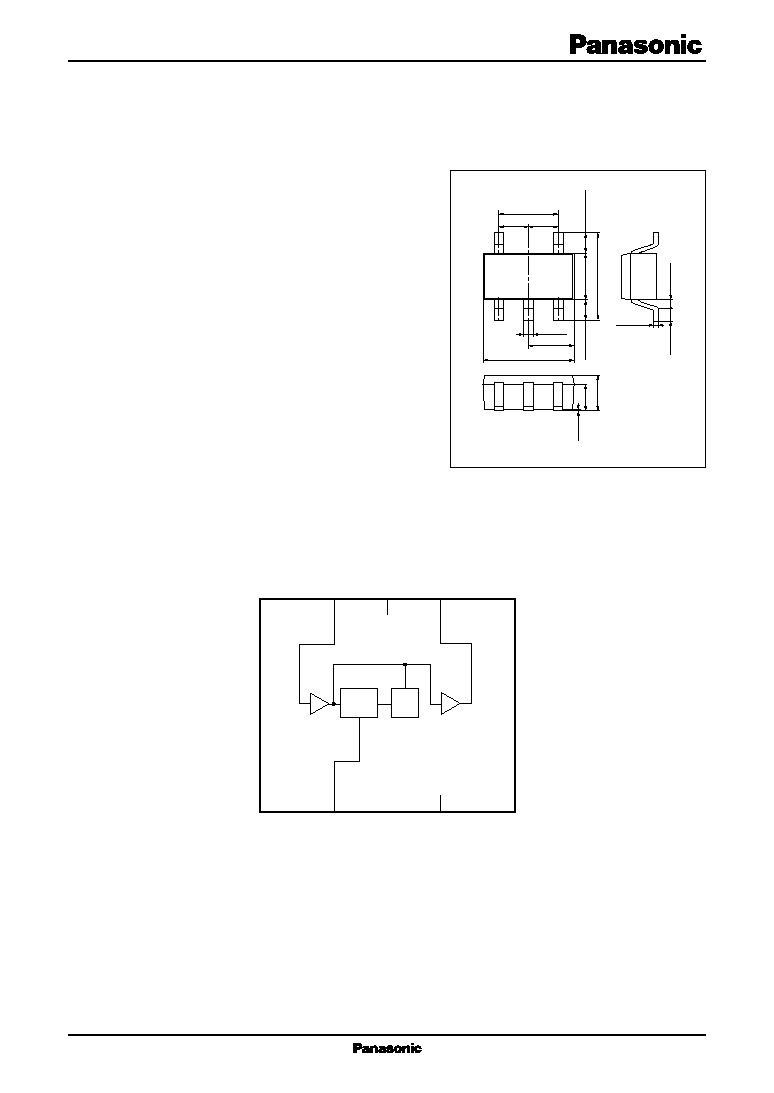
MINI-5D
Unit: mm
5
1
4
3
2
DET
g
m
V
CC
Output
GND
DET
Input
2.8
1.5
3
5
4
1.9 ±
0.1
+ 0.2
-
0.3
0.16
+ 0.10
-
0.06
0.4 ±
0.2
0.95
0.95
0.3
+ 0.1
-
0.05
0.1 to 0.3
-
0.05
1.45 ±
0.1
2.9
+ 0.2
0 to 0.1
0.8
1.1
+ 0.2
-
0.1
1
2
0.65 ±
0.15
0.65 ±
0.15
+ 0.25
-
0.05
2
AN6213MS
ICs for Telephone
s
Pin Descriptions
Pin No.
Description
1
V
CC
Supply voltage pin
2
DET
Detection pin
3
Input
Signal input pin
4
GND
Grounding pin
5
Output
Signal output pin
Parameter
Symbol
Conditions
Min
Typ
Max
Unit
Operating current
I
CC
Without signal input
450
900
µ
A
s
Electrical Characteristics at V
CC
=
3.0 V, f
=
1 kHz, T
a
=
25
°
C
s
Absolute Maximum Ratings
Parameter
Symbol
Rating
Unit
Supply voltage
V
CC
6.5
V
Supply current
I
CC
3.0
mA
Power dissipation
P
D
19.5
mW
Operating ambient temperature
*
T
opr
-
20 to
+
75
°
C
Storage temperature
*
T
stg
-
55 to
+
125
°
C
Note) *: Except for the operating ambient temperature and storage temperature, all ratings are for T
a
=
25
°
C.
s
Recommended Operating Range
Parameter
Symbol
Range
Unit
Supply voltage
V
CC
2.4 to 6.0
V
Parameter
Symbol
Conditions
Min
Typ
Max
Unit
Voltage gain
G
V
V
IN
=
-40
dBm
22
24
26
dB
Output level
V
O
V
IN
=
-
10 dBm
-
9.5
-
7.5
-
5.5
dBm
ALC control range
ALC
Output level varying amount
-
1.5
1.5
dB
at V
IN
=
-
25 dBm, V
IN
=
0
dBm
Total harmonic distortion factor
THD
At V
IN
=
-
10 dBm
1
3
%
Output noise voltage
V
NO
Terminated by CCIT filter input 2 k
-
70
-
60
dBm
Input impedance
Z
IN
Pin 3 input impedance
15
30
45
k
Output impedance
Z
OUT
Pin 5 output impedance
200
400
600
·
Design reference data
Note) The characteristics listed below are theoretical values based on the IC design and are not guaranteed.
3
ICs for Telephone
AN6123MS
s
Application Notes
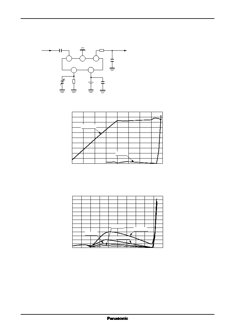
1. I/O characteristics and distortion
The I/O characteristics in the circuit shown
on the left can be referred to in the graph below.
Also note that if the C in the circuit is lowered,
the distortion characteristics will become worse
(Graph 2).
GND
10 k
2 200 pF
33
µ
F
10
µ
F
C
1 M
3.0 V
Signal output
Signal input
(Input frequency
=
1 kHz)
4
3
2
5
1
AN6123MS
Graph 1. I/O characteristics and distortion (when C
=
10
µ
F)
-
50
0
2
4
6
8
10
12
-
70
-
60
-
50
-
40
-
30
-
20
-
10
0
10
-
45
-
40
-
35
-
30
-
25
-
20
-
15
-
10
-
5
0
Output le
v
el (dBm)
Distortion (
%
)
Input level (dBm)
Output level
Distortion
Graph 2. Distortion characteristics when C is variable
0
-
40
-
35
-
30
-
25
-
20
-
15
-
10
-
5
0
5
10
1
2
4
3
5
6
7
8
9
10
11
12
13
Distortion (
%
)
Input lebve; (dBm)
C
=
4.7
µ
F
C
=
10
µ
F
C
=
1.0
µ
F
C
=
2.2
µ
F
4
AN6213MS
ICs for Telephone
s
Application Notes (continued)
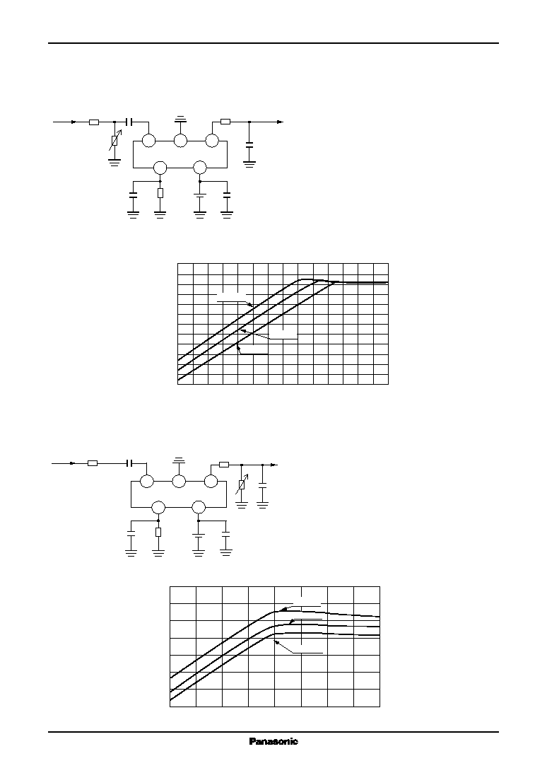
2. Input level adjustment for maximum output
You can adjust R in the left circuit diagram
to find the operation point for a maximum out-
put level. For example, since the input level for
a maximum output is
-
30 dBm when R is open
and the attenuation in the input stage is 20 log
(3k/6.3k)
=
-
6.4 dB when R is 3 k
. This means
a total gain loss is
-
6.4 dB as compared with
open mode, hence the input level to get the
maximum output is
-
23.6 dBm.
Likewise, the attenuation is 12.7 dB for R
=
1 k
and the desired input level becomes 17.3
dBm.
I/O characteristics
GND
10 k
2 200 pF
33
µ
F
10
µ
F
10
µ
F
1M
3.0 V
Signal input
(1 kHz)
4
3
2
5
1
AN6123MS
R
3.3 k
Signal output
-
60
-
70
-
65
-
60
-
55
-
50
-
45
-
40
-
35
-
30
-
25
-
20
-
15
-
10
-
5
0
-
55
-
50
-
40
-
45
-
35
-
30
-
25
-
20
-
15
-
10
-
5
0
Output le
v
el (dBm)
Input level (dBm)
R
=
3 k
R
=
Open
R
=
1 k
3. Output level adjustment for a maximum output
The maximum output level can be adjusted
by R in the left circuit diagram.
Since the maximum output is
-
7.5 dBm
when R is open, it is 20 log (20k/30k)
=
-
3.5
dBm at R
=
20 k
. It is an attenuated value of by
3.4 dB against open mode. Therefore, the maxi-
mum output becomes
-
11 dBm. Likewise, for R
=
10 k
, attenuation is 6 dB and the maximum
output becomes
-
13.5 dBm.
I/O characteristics
-
35
-
30
-
25
-
20
-
15
-
10
-
5
0
-
50
-
45
-
40
-
35
-
30
-
25
-
20
-
15
-
10
Output le
v
el (dBm)
Input level (dBm)
R
=
10 k
R
=
Open
R
=
20 k
GND
10 k
2 200 pF
33
µ
F
10
µ
F
10
µ
F
1M
3.0 V
Signal output
Signal input
(1 kHz)
4
3
2
5
1
AN6123MS
R
3.3 k
5
ICs for Telephone
AN6123MS
s
Application Notes (continued)
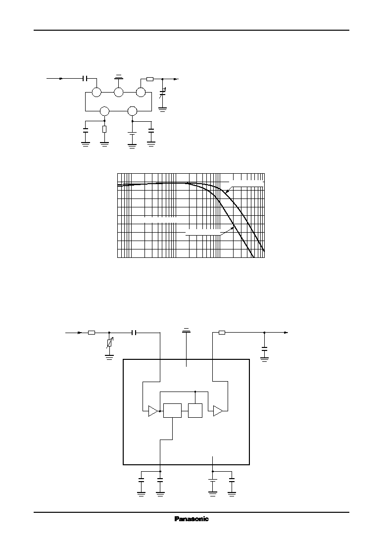
4. Frequency characteristics
The AN6123MS itself has an almost flat fre-
quency characteristic in the audio frequency band.
The high-band frequency is set with R and C
shown in the left circuit. The cut-off frequency f
C
at R
=
10 k
and C
=
2 200 pF, that is the frequency
at which the frequency characteristic deteriorates
by 3 dB, is f
C
=
1/2
CR
=
7.2 kHz. At R
=
10 k
and C
=
1 000 pF, it is 16 kHz. (Refer to the graph.)
Frequency characteristics
GND
10 k
33
µ
F
10
µ
F
10
µ
F
1 M
3.0 V
4
3
2
5
1
AN6123MS
R
C
Signal output
Signal input
Input frequency (Hz)
Gain
(dB)
100
1k
10k
100k
-
10
-
8
-
6
-
4
-
2
0
2
4
6
8
10
For C
=
1 000 pF
For C
=
2 200 pF
Input signal level:
-
10 dBm
s
Application Circuit Example
V
CC
GND
10 k
3.3 k
2 200 pF
33
µ
F
10
µ
F
10
µ
F
1 M
2.4 V
6.0 V
G
=
30 dB
Signal output
0.9 V[p-p]
Noise
=
-
70 dBm
Distortion
=
1
%
Signal input
(300 Hz
3 kHz)
R
5
1
4
3
2
DET
g
m